Yamaha MG102c Service Manual
Hide thumbs
Also See for MG102c:
- Owner's manual (21 pages) ,
- Manual de usuario (21 pages) ,
- Manuel du propriétaire (21 pages)
Table of Contents
Advertisement
QQ
3 7 63 1515 0
TE
L 13942296513
www
.
PA
011846
MG82CX: 200702-29190
MG102C: 200702-20790
http://www.xiaoyu163.com
CONTENTS
BLOCK DIAGRAM
x
ao
u163
y
i
2 9
8
MIXING CONSOLE
SERVICE MANUAL
SERVICE MANUAL
Q Q
3
6 7
1 3
1 5
MG82CX
............................................................9
.......................................................32/39
co
.
Copyright (c) Yamaha Corporation. All rights reserved. PDF
9 4
2 8
0 5
8
2 9
9 4
2 8
..............................................3/6
.................9
....................................10
.............14
............................16
.............................20
..................................21
.........................................23
m
HAMAMATSU, JAPAN
9 9
9 9
MG102C
'07.01
&
Advertisement
Table of Contents

Related Manuals for Yamaha MG102c


Summary of Contents for Yamaha MG102c
-
Page 1: Mixing Console
DISASSEMBLY PROCEDURE ......16 LSI PIN DESCRIPTION ......20 IC BLOCK DIAGRAM ........21 CIRCUIT BOARD .........23 INSPECTIONS ............32/39 PARTS LIST BLOCK DIAGRAM CIRCUIT DIAGRAM u163 011846 HAMAMATSU, JAPAN MG82CX: 200702-29190 MG102C: 200702-20790 Copyright (c) Yamaha Corporation. All rights reserved. PDF ’07.01 &... - Page 2 IMPORTANT NOTICE This manual has been provided for the use of authorized Yamaha Retailers and their service personnel. It has been assumed that basic service procedures inherent to the industry, and more specifically Yamaha Products, are already known and understood by the users, and have therefore not been restated.
-
Page 3: Specifications
Dimensions (W x H x D) Net Weight 1.6 kg (MG82CX), 1.5 kg (MG102C) All level controls are nominal if not specified. Output impedance of signal generator: 150 ohms u163 The MG82CX feature is described first, followed by the MG102C feature in brackets: MG82CX (MG102C) - Page 4 100 Ω 40 Ω Phones 3 mW 75 mW Stereo phone jack Where 0 dBu = 0.775 Vrms and 0 dBV= 1 Vrms * The MG82CX feature is described first, followed by the MG102C feature in brackets: MG82CX (MG102C) u163...
-
Page 5: Digital Effect Program List
MG82CX/MG102C 3 7 63 1515 0 Digital Effect Program List Program Parameter Description REVERB HALL 1 REVERB TIME Reverb simulating a large space such as a concert hall. REVERB HALL 2 REVERB TIME REVERB ROOM 1 REVERB TIME Reverb simulating the acoustics of a small space (room). - Page 6 MG82CX/MG102C 3 7 63 1515 0 L 13942296513 u163...
- Page 7 MG82CX/MG102C 3 7 63 1515 0 L 13942296513 u163...
- Page 8 MG82CX/MG102C 3 7 63 1515 0 L 13942296513 u163...
- Page 9 MG82CX/MG102C 3 7 63 1515 0 CIRCUIT BOARD LAYOUT MAIN8 JACK (MG82CX) MAIN10 JACK (MG102C) MAIN8 MAIN (MG82CX) MAIN10 MAIN (MG102C) Bottom case assembly (MG82CX only) L 13942296513 DIMENSIONS 62.2 256.6 55.2 u163...
-
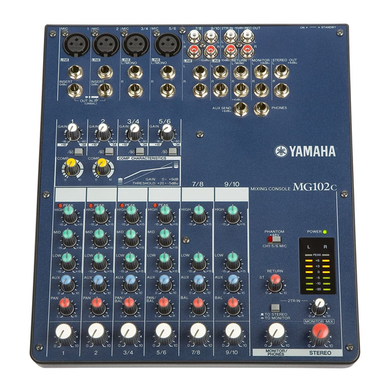
Page 10: Panel Layout
PANEL LAYOUT The following applies to both the MG82CX and MG102C. In cases where different features need to be described for each model, the MG82CX feature will be described fi rst, followed by the MG102C feature in brackets: MG82CX (MG102C). - Page 11 MG82CX/MG102C 3 7 63 1515 0 Master Control Section q 2TR IN Jacks w REC OUT (L, R) Jacks e RETURN L (MONO), R Jacks r SEND EFFECT (AUX) Jack t STEREO OUT (L, R) Jacks y MONITOR (L, R) Jacks...
- Page 12 MG82CX/MG102C 3 7 63 1515 0 DIGITAL EFFECT Rear Input/Output Section * Only the MG82CX has digital effects. L 13942296513 DIGITAL EFFECT q FOOT SWITCH Jack w PROGRAM Dial e PARAMETER Control r ON Switch t EFFECT RTN Control...
-
Page 13: Jack List
MG82CX/MG102C 3 7 63 1515 0 Jack List Input and Output Jacks Polarities Configurations MIC INPUT Pin 1: Ground Pin 2: Hot (+) INPUT OUTPUT Pin 3: Cold (–) LINE INPUT(CHs 1, 2) Tip: Hot (+) STEREO OUT, MONITOR OUT, Ring: Cold (–) -
Page 14: General Schematic Diagram
MG82CX/MG102C 3 7 63 1515 0 GENERAL SCHEMATIC DIAGRAM Processing Method of Wiring Assembly AC (WH54770) (a). Bundle three wires and fi x them with the cord holder (location: 300) at a position 20 mm away from the component side of the circuit board. - Page 15 MG82CX/MG102C 3 7 63 1515 0 (a). Bend the jumper leads to make an M-like fi gure. (b). After bending as mentioned above, deal with the jumper leads until the distance between their top end and the MIX circuit board surface is 15 mm or less.
-
Page 16: Disassembly Procedure
MG82CX/MG102C 3 7 63 1515 0 DISASSEMBLY PROCEDURE • MG82CX Top Cover (Time required: About 7 minutes) Remove all knobs. (Fig. 1) Remove the fourteen (14) screws marked [160], the screw marked [163A], the screw marked [165], and nineteen (19) each hexagonal nuts and washers marked [A]. - Page 17 MG82CX/MG102C 3 7 63 1515 0 DSP Circuit Board 2-3-1 Reverse the MAIN8 circuit board and remove the two (2) screws marked [80]. The DSP circuit board can then be pulled out. (Fig. 2) MAIN8 Circuit Board 2-4-1 Remove the spacer on the upper side of the MAIN8 circuit board.
- Page 18 MG82CX/MG102C 3 7 63 1515 0 DISASSEMBLY PROCEDURE • MG102C Top Cover (Time required: About 7 minutes) Remove all knobs. (Fig. 1) Remove the fourteen (14) screws marked [160], the screw marked [163A], and twenty (20) each hexagonal nuts and washers marked [A]. The top cover can then be removed.
- Page 19 MG82CX/MG102C 3 7 63 1515 0 Remove the knob joints and push buttons from the MAIN10 circuit board. (Fig. 2) The knob joints and push buttons are not com- ponents of the MAIN10 circuit board. When replacing the MAIN10 circuit board, remove the knob joints and push buttons and install them on the new MAIN10 circuit board.
-
Page 20: Lsi Pin Description
MG82CX/MG102C 3 7 63 1515 0 LSI PIN DESCRIPTION YMW767-VTZ (X6055A00) CPU (SWL01B) DSP: ICM07 NAME FUNCTION NAME FUNCTION Ground Ground Input for TEST Power supply +3.3 V TESTN PLLBPN PLL bypass select External memory lower-byte enable / Port F... -
Page 21: Ic Block Diagram
IC553, IC801, IC803, IC804, IC901 MAIN8: IC302, IC402 (MG82CX) MAIN10: IC102, IC103, IC105, IC151, IC152, DSP : ICM09, ICM11 (MG82CX) (MG102C) IC301, IC351, IC352, IC401, IC451, MAIN8: IC104, IC808 (MG82CX) IC452, IC501-504, IC551-554, MAIN10: IC101 (MG102C) IC801-804 MAIN10: IC302, IC402 (MG102C) - Page 22 MG82CX/MG102C 3 7 63 1515 0 PCM1742KEG/2K (X3538A00) DSP : ICM08 (MG82CX) Digital to Analog Converter DATA LRCK DGND ZEROL/NA Audio LRCK Output Amp and Serial ZEROR/ZEROA Port Low-Pass Filter 4x/8x DATA Enhanced Oversampling Multilevel Digital Filter AGND Delta-Sigma...
- Page 23 MAIN8 (JACK) Circuit Board (X7686D0) (MG82CX) ....... 24 MAIN8 (MAIN) Circuit Board (X7686D0) (MG82CX) ....... 26 MAIN10 (JACK) Circuit Board (X7685D0) (MG102C) ......28 MAIN10 (MAIN) Circuit Board (X7685D0) (MG102C) ......30 Note: See parts list for details of circuit board component parts.
-
Page 24: Circuit Board
MG82CX/MG102C 3 7 63 1515 0 MAIN8 (JACK) Circuit Board (MG82CX) Scale: 95/100 COMP GAIN (CH1) (CH1) (CH1) COMP GAIN (CH2) (CH2) (CH2) GAIN (CH3/4) (CH3/4) GAIN (CH5/6) (CH5/6) L 13942296513 u163 Component side 2NA-WH10830-... - Page 25 MG82CX/MG102C 3 7 63 1515 0 MAIN8 (JACK) Circuit Board (MG82CX) Scale: 95/100 L 13942296513 u163 Pattern side 2NA-WH10830-...
- Page 26 MG82CX/MG102C 3 7 63 1515 0 MAIN8 (MAIN) Circuit Board (MG82CX) Scale: 95/100 PEAK EFFECT HIGH PAN (CH1) (CH1) (CH1) (CH1) (CH1) PEAK EFFECT HIGH PAN (CH2) (CH2) (CH2) (CH2) (CH2) PEAK PAN/BAL EFFECT HIGH (CH3/4) (CH3/4) (CH3/4) (CH3/4)
- Page 27 MG82CX/MG102C 3 7 63 1515 0 MAIN8 (MAIN) Circuit Board (MG82CX) Scale: 95/100 L 13942296513 u163 Pattern side 2NA-WH10830-...
- Page 28 MG82CX/MG102C 3 7 63 1515 0 MAIN10 (JACK) Circuit Board (MG102C) Scale: 95/100 COMP GAIN (CH1) (CH1) (CH1) COMP GAIN (CH2) (CH2) (CH2) GAIN (CH3/4) (CH3/4) GAIN (CH5/6) (CH5/6) L 13942296513 u163 Component side 2NA-WH10820-...
- Page 29 MG82CX/MG102C 3 7 63 1515 0 MAIN10 (JACK) Circuit Board (MG102C) Scale: 95/100 L 13942296513 u163 Pattern side 2NA-WH10820-...
- Page 30 MG82CX/MG102C 3 7 63 1515 0 MAIN10 (MAIN) Circuit Board (MG102C) Scale: 95/100 PEAK PAN (CH1) HIGH (CH1) (CH1) (CH1) (CH1) PEAK PAN (CH2) HIGH (CH2) (CH2) (CH2) (CH2) PEAK HIGH PAN (CH3/4) (CH3/4) (CH3/4) (CH3/4) (CH3/4) PEAK HIGH...
- Page 31 MG82CX/MG102C 3 7 63 1515 0 MAIN10 (MAIN) Circuit Board (MG102C) Scale: 95/100 L 13942296513 u163 Pattern side 2NA-WH10820-...
- Page 32 Minimum AUX level control (MG102C) Minimum PAN/BAL control L (Turned counterclockwise fully) CH level control Maximum • ST CH INPUT (CH7/8, CH9/10 (MG102C)) EQ gain control (HIGH, LOW) Center EFFECT level control (MG82CX) Minimum AUX level control (MG102C) Minimum BAL control...
- Page 33 INPUT ST OUT L ST OUT R level control AUX SEND (MG102C) OUT L OUT R –72.0 dBu Maximum +1.5 dBu ± 2.0 dB *1 +1.5 dBu ± 2.0 dB *1 +4.5 dBu ± 2.0 dB *2 +18.5 dBu ± 2.0 dB *1 +18.5 dBu ± 2.0 dB *1...
- Page 34 20 Hz. * For the signal path q, check the ST OUT L, R and EFFECT SEND (AUX SEND in case of MG102C) when the signal is input to CH1, and check only the ST OUT L when the signal is input to CH2.
- Page 35 ±20% and check that the output level of the ST OUT L, R is within the range shown in Table 2-9-1. * When the signal is input to CH1, CH2, CH7 L or CH9 L (MG102C), measure the output level at the ST OUT L.
- Page 36 Check that the distortion is 1.0% or less when the output level of the ST OUT L, R, EFFECT SEND (AUX SEND in case of MG102C), and MONITOR OUT L, R is set to +20.0 dBu. Check that the distortion is 1.0% or less when the output level at the PHONES L, R is set to +7.5 dBu.
- Page 37 MG82CX/MG102C 3 7 63 1515 0 2-17-3 Frequency characteristic Under the setting of Table 2-17-2, check that the output level at the INSERT OUT 1, 2 when the signal frequency is set to 20 Hz and 20 kHz is within the range of ±3.0 dB compared with the output level when the signal frequency is set to 1 kHz.
- Page 38 MG82CX/MG102C 3 7 63 1515 0 2-18 Digital effect (MG82CX) Set each volume of CH1, MASTER and DIGITAL EFFECT as follows, • CH INPUT (CH1) EFFECT level control Maximum CH level control Maximum • MASTER STEREO level control Maximum •...
- Page 39 MG82CX/MG102C 3 7 63 1515 0 L 13942296513 u163...
- Page 40 MONITOR INPUT ST OUT L ST OUT R level control AUX SEND (MG102C) OUT L OUT R –72.0 dBu +1.5 dBu ± 2.0 dB *1 +1.5 dBu ± 2.0 dB *1 +4.5 dBu ± 2.0 dB *2 +18.5 dBu ± 2.0 dB *1 +18.5 dBu ± 2.0 dB *1 1, 2 –28.0 dBu...
- Page 41 3 7 63 1515 0 Input GAIN EFFECT SEND (MG82CX) INPUT ST OUT L ST OUT R level control AUX SEND (MG102C) +4.5 dBu ± 2.0 dB — 9 L (MG102C) PHONE +1.5 dBu ± 2.0 dB (LINE) — +4.5 dBu ± 2.0 dB 10 R (MG102C) –22.0 dBu...
- Page 42 +15.0 dB ± 2.0 dB PHONE 5 L/MONO 2.5 kHz (LINE) 7 L, 8 R –15.0 dB ± 2.0 dB 9 L (MG102C), +12.0 dB ± 2.0 dB 10 R (MG102C) 100 Hz –12.0 dB ± 2.0 dB L 13942296513 INPUT PEAK LED 1–5/6...
- Page 43 MG82CX/MG102C 3 7 63 1515 0 L 13942296513 MASTER ST OUT EFFECT SEND (MG82CX) MONITOR OUT volume (L, R) AUX SEND (MG102C) (L, R) –81.0 dBu –85.0 dBu –78.0 dBu –100.0 dBu — –93.0 dBu Input COMP INSERT OUT...
- Page 44 MG82CX/MG102C 3 7 63 1515 0 Input Distortion Frequency 20 Hz 5.0 % 1 kHz 1.0 % 20 kHz 1.0 % ATTACK TIME RELEASE TIME L 13942296513 100% 100% Restoration Time Restoration Time INSERT OUT (1, 2) Attack time...
- Page 45 MG82CX/MG102C 3 7 63 1515 0 L 13942296513 u163...
-
Page 46: Parts List
http://www.xiaoyu163.com 3 7 63 1515 0 MIXING CONSOLE PARTS LIST CONTENTS OVERALL ASSEMBLY ....2 OVERALL ASSEMBLY ....4 ELECTRICAL PARTS ....6 ELECTRICAL PARTS ..... 20 L 13942296513 Notes : DESTINATION ABBREVIATIONS A : Australian model M : South African model B : British model O : Chinese model C : Canadian model... - Page 47 MG82CX/MG102C 3 7 63 1515 0 OVERALL ASSEMBLY (MG82CX) JACK L 13942296513 MAIN 8 input channels 4 mic + 3 stereo line inputs 2 insert I/O Phantom powet switch (+ 48V) 3 band (CH 1-5/6)/ 2 band (CH 7/8) EQ 3 busses (stereo + +effect) 1 effect send &...
- Page 48 MG82CX/MG102C 3 7 63 1515 0 PART NO. DESCRIPTION REMARKS REF NO. RANK OVERALL ASSEMBLY MG82CX Overall Assembly (WH10100) WJ351600 Bottom Case Assembly WH108400 Circuit Board Shield DSP (WH10070) WE774300 Bind Head Tapping Screw-B 3.0X8 MFZN2W3 WH108300 Circuit Board...
- Page 49 MG82CX/MG102C 3 7 63 1515 0 OVERALL ASSEMBLY (MG102C) JACK MAIN L 13942296513 10 input channels 4 mic + 4 stereo line inputs 2 insert I/O Phantom powet switch (+ 48V) 3 band (CH 1-5/6)/ 2 band (CH 7/8-9/10) EQ 3 busses (stereo + aux) 1 Aux send &...
- Page 50 MG82CX/MG102C 3 7 63 1515 0 PART NO. DESCRIPTION REMARKS REF NO. RANK OVERALL ASSEMBLY MG102C Overall Assembly (WH09040) WJ351600 Bottom Case Assembly WH108200 Circuit Board MAIN10 WE774300 Bind Head Tapping Screw-B 3.0X8 MFZN2W3 WH362000 Knob Joint WD942200 Knob Joint...
- Page 51 MG82CX/MG102C 3 7 63 1515 0 ELECTRICAL PARTS (MG82CX) PART NO. DESCRIPTION REMARKS REF NO. RANK ELECTRICAL PARTS MG82CX WH108400 Circuit Board (WH10870)(X7687D0) WH108300 Circuit Board MAIN8 (X7686D0) WH108400 Circuit Board (WH10870)(X7687D0) CM01 US064100 Ceramic Capacitor-B (chip) 0.0100 50V K RECT.
- Page 52 MG82CX/MG102C 3 7 63 1515 0 DSP and MAIN8 PART NO. DESCRIPTION REMARKS REF NO. RANK * ICM12 X8138A00 IC TAR5S25U(TE85L,F) REGULATOR +2.5V JMM02 RD350000 Carbon Resistor (chip) 0 63M J RECT. RD350000 Carbon Resistor (chip) 0 63M J RECT.
- Page 53 MG82CX/MG102C 3 7 63 1515 0 MAIN8 PART NO. DESCRIPTION REMARKS REF NO. RANK US065100 Ceramic Capacitor-F (chip) 0.100 50V Z RECT. UR857470 Electrolytic Cap. 47.00 35.0V RX TP US065100 Ceramic Capacitor-F (chip) 0.100 50V Z RECT. UR857470 Electrolytic Cap.
- Page 54 MG82CX/MG102C 3 7 63 1515 0 MAIN8 PART NO. DESCRIPTION REMARKS REF NO. RANK C215 UA654820 Mylar Capacitor 0.0820 50V J RX TP C216 US062100 Ceramic Capacitor-SL(chip) 100P 50V J RECT. C217 UR867100 Electrolytic Cap. 10.00 50.0V RX TP C218 UR857470 Electrolytic Cap.
- Page 55 MG82CX/MG102C 3 7 63 1515 0 MAIN8 PART NO. DESCRIPTION REMARKS REF NO. RANK C403 WH167700 Electrolytic Cap. 10.00 50.0V TATETP C404 WH167700 Electrolytic Cap. 10.00 50.0V TATETP C405 UR867100 Electrolytic Cap. 10.00 50.0V RX TP C406 UR867100 Electrolytic Cap.
- Page 56 MG82CX/MG102C 3 7 63 1515 0 MAIN8 PART NO. DESCRIPTION REMARKS REF NO. RANK C536 US061220 Ceramic Capacitor-CH(chip) 22P 50V J RECT. C537 US061220 Ceramic Capacitor-CH(chip) 22P 50V J RECT. C538 US064100 Ceramic Capacitor-B (chip) 0.0100 50V K RECT.
- Page 57 MG82CX/MG102C 3 7 63 1515 0 MAIN8 PART NO. DESCRIPTION REMARKS REF NO. RANK C861 UR838100 Electrolytic Cap. 100.00 16.0V RX TP C901 US063100 Ceramic Capacitor-B (chip) 1000P 50V K RECT. C904 US062220 Ceramic Capacitor-SL(chip) 220P 50V J RECT.
- Page 58 MG82CX/MG102C 3 7 63 1515 0 MAIN8 PART NO. DESCRIPTION REMARKS REF NO. RANK * JK403 WH919000 Phone Jack ST MSJ-064-30B B LINE R(CH5/6) * JK501 WH919000 Phone Jack ST MSJ-064-30B B LINE L(CH7/8) * JK502 WH919000 Phone Jack...
- Page 59 MG82CX/MG102C 3 7 63 1515 0 MAIN8 PART NO. DESCRIPTION REMARKS REF NO. RANK R119 RF354150 Carbon Resistor (chip) 15.0 D 1608 R120 RF356820 Carbon Resistor (chip) 8.2K D 1608 R121 RF356220 Carbon Resistor (chip) 2.2K D 1608 R123 RF357270 Carbon Resistor (chip) 27.0K D 1608...
- Page 60 MG82CX/MG102C 3 7 63 1515 0 MAIN8 PART NO. DESCRIPTION REMARKS REF NO. RANK R231 RD358100 Carbon Resistor (chip) 100.0K 63M J RECT. R232 RD357270 Carbon Resistor (chip) 27.0K 63M J RECT. R233 RD355820 Carbon Resistor (chip) 820.0 63M J RECT.
- Page 61 MG82CX/MG102C 3 7 63 1515 0 MAIN8 PART NO. DESCRIPTION REMARKS REF NO. RANK -366 RD356270 Carbon Resistor (chip) 2.7K 63M J RECT. R367 RD358100 Carbon Resistor (chip) 100.0K 63M J RECT. R368 RD357100 Carbon Resistor (chip) 10.0K 63M J RECT.
- Page 62 MG82CX/MG102C 3 7 63 1515 0 MAIN8 PART NO. DESCRIPTION REMARKS REF NO. RANK R483 RD356470 Carbon Resistor (chip) 4.7K 63M J RECT. R484 RD356470 Carbon Resistor (chip) 4.7K 63M J RECT. R487 RD357180 Carbon Resistor (chip) 18.0K 63M J RECT.
- Page 63 MG82CX/MG102C 3 7 63 1515 0 MAIN8 PART NO. DESCRIPTION REMARKS REF NO. RANK R834 RD356100 Carbon Resistor (chip) 1.0K 63M J RECT. R835 RD357100 Carbon Resistor (chip) 10.0K 63M J RECT. -838 RD357100 Carbon Resistor (chip) 10.0K 63M J RECT.
- Page 64 MG82CX/MG102C 3 7 63 1515 0 MAIN8 PART NO. DESCRIPTION REMARKS REF NO. RANK RJ19 RD350000 Carbon Resistor (chip) 0 63M J RECT. * SW101 WH918700 Push Switch PS-22E85L-02 (CH1) * SW201 WH918700 Push Switch PS-22E85L-02 (CH2) * SW301 WH918700 Push Switch...
- Page 65 MG82CX/MG102C 3 7 63 1515 0 ELECTRICAL PARTS (MG102C) MAIN10 PART NO. DESCRIPTION REMARKS REF NO. RANK ELECTRICAL PARTS MG102C WH108200 Circuit Board MAIN10 (X7685D0) WH108200 Circuit Board MAIN10 (X7685D0) Silicon Grease G-746 (0412125) Jumper Wire 0.55 TIN (VA07890)
- Page 66 MG82CX/MG102C 3 7 63 1515 0 MAIN10 PART NO. DESCRIPTION REMARKS REF NO. RANK C164 US062100 Ceramic Capacitor-SL(chip) 100P 50V J RECT. C165 US061470 Ceramic Capacitor-CH(chip) 47P 50V J RECT. C166 UR857470 Electrolytic Cap. 47.00 35.0V RX TP C167 US064100 Ceramic Capacitor-B (chip) 0.0100 50V K RECT.
- Page 67 MG82CX/MG102C 3 7 63 1515 0 MAIN10 PART NO. DESCRIPTION REMARKS REF NO. RANK C358 UA654120 Mylar Capacitor 0.0120 50V J RX TP C359 UA653390 Mylar Capacitor 3900P 50V J RX TP C360 UA653390 Mylar Capacitor 3900P 50V J RX TP...
- Page 68 MG82CX/MG102C 3 7 63 1515 0 MAIN10 PART NO. DESCRIPTION REMARKS REF NO. RANK -504 UR867100 Electrolytic Cap. 10.00 50.0V RX TP C505 US062100 Ceramic Capacitor-SL(chip) 100P 50V J RECT. -512 US062100 Ceramic Capacitor-SL(chip) 100P 50V J RECT. C513 US061470 Ceramic Capacitor-CH(chip) 47P 50V J RECT.
- Page 69 MG82CX/MG102C 3 7 63 1515 0 MAIN10 PART NO. DESCRIPTION REMARKS REF NO. RANK -823 UR867100 Electrolytic Cap. 10.00 50.0V RX TP C828 US062100 Ceramic Capacitor-SL(chip) 100P 50V J RECT. -831 US062100 Ceramic Capacitor-SL(chip) 100P 50V J RECT. C832 US061680 Ceramic Capacitor-SL(chip) 68P 50V J RECT.
- Page 70 MG82CX/MG102C 3 7 63 1515 0 MAIN10 PART NO. DESCRIPTION REMARKS REF NO. RANK * JK303 WH919000 Phone Jack ST MSJ-064-30B B LINE R(CH3/4) * JK401 WG848700 Cannon Connector JACK NC3FAAV2-0-Y MIC(CH5/6) * JK402 WH919000 Phone Jack ST MSJ-064-30B B...
- Page 71 MG82CX/MG102C 3 7 63 1515 0 MAIN10 PART NO. DESCRIPTION REMARKS REF NO. RANK R116 RF356220 Carbon Resistor (chip) 2.2K D 1608 R117 RF356820 Carbon Resistor (chip) 8.2K D 1608 R119 RF354150 Carbon Resistor (chip) 15.0 D 1608 R120 RF356820 Carbon Resistor (chip) 8.2K D 1608...
- Page 72 MG82CX/MG102C 3 7 63 1515 0 MAIN10 PART NO. DESCRIPTION REMARKS REF NO. RANK R229 RD358220 Carbon Resistor (chip) 220.0K 63M J RECT. R230 RD357560 Carbon Resistor (chip) 56.0K 63M J RECT. R231 RD358100 Carbon Resistor (chip) 100.0K 63M J RECT.
- Page 73 MG82CX/MG102C 3 7 63 1515 0 MAIN10 PART NO. DESCRIPTION REMARKS REF NO. RANK R363 RD356270 Carbon Resistor (chip) 2.7K 63M J RECT. -366 RD356270 Carbon Resistor (chip) 2.7K 63M J RECT. R367 RD358100 Carbon Resistor (chip) 100.0K 63M J RECT.
- Page 74 MG82CX/MG102C 3 7 63 1515 0 MAIN10 PART NO. DESCRIPTION REMARKS REF NO. RANK R481 RD357220 Carbon Resistor (chip) 22.0K 63M J RECT. R482 RD357220 Carbon Resistor (chip) 22.0K 63M J RECT. R483 RD356470 Carbon Resistor (chip) 4.7K 63M J RECT.
- Page 75 MG82CX/MG102C 3 7 63 1515 0 MAIN10 PART NO. DESCRIPTION REMARKS REF NO. RANK -806 RD357180 Carbon Resistor (chip) 18.0K 63M J RECT. R807 RD357680 Carbon Resistor (chip) 68.0K 63M J RECT. R808 RD357390 Carbon Resistor (chip) 39.0K 63M J RECT.
- Page 76 MG82CX/MG102C 3 7 63 1515 0 MAIN10 PART NO. DESCRIPTION REMARKS REF NO. RANK * SW201 WH918700 Push Switch PS-22E85L-02 (CH2) * SW301 WH918700 Push Switch PS-22E85L-02 (CH3/4) * SW401 WH918700 Push Switch PS-22E85L-02 (CH5/6) * SW551 WH918800 Push Switch...
-
Page 77: Note: See Parts List For Details Of Circuit Board Component Parts
3 7 63 1515 0 MIXING CONSOLE CIRCUIT DIAGRAM CONTENTS BLOCK DIAGRAM (MG82CX) ..3 BLOCK DIAGRAM (MG102C) ..4 CIRCUIT DIAGRAM (MG82CX) ................5 (MG82CX) ..............6 (MG102C) ..............12 L 13942296513 Notation for Circuit Diagrams 1. How to identify inter-sheet connectors This indicates the location of the counter inter-sheet connector. - Page 78 BLOCK DIAGRAM (MG82CX) 3 7 6 3 1 5 1 5 0 MG82CX/MG102C PHANTOM JACK MAIN MAIN8 MAIN8 MAIN8 SW801 JACK JK101, JK201 PEAK +48V LD815 (CH1, CH2) IC101 (8P) IC103 (8P), LD151, SW101, LD251 IC104 (8P), ST CH LEVEL [–60 to –16dBu]...
- Page 79 BLOCK DIAGRAM (MG102C) 3 7 6 3 1 5 1 5 0 MG82CX/MG102C PHANTOM JACK MAIN MAIN10 MAIN10 MAIN10 SW801 JACK +48V JK101, JK201 PEAK LD815 (CH1, CH2) LD151, IC101 (8P) IC103 (8P), SW101, LD251 IC104 (8P), ST CH LEVEL IC802 (8P) [–60 to –16dBu]...
- Page 80 DSP CIRCUIT DIAGRAM (MG82CX) 3 7 6 3 1 5 1 5 0 MG82CX/MG102C TAR5S33 (XZ642A00) REGULATOR +3.3V DSP: ICM06 SYSTEM RESET 1: CONTROL 2: GND 3: NOISE 4: V 5: V TAR5S25U (X8138A00) REGULATOR +2.5V DSP: ICM12 MASK ROM...
- Page 81 MAIN8 (JACK) CIRCUIT DIAGRAM (MG82CX) 001 3 7 6 3 1 5 1 5 0 MG82CX/MG102C OP AMP MA111 (VR496500) MAIN8: D101-103, D201-203 MIC (CH1) [–60 to –16dBu] OP AMP OP AMP OP AMP LINE (CH1) [–34 to +10dBu]...
- Page 82 MAIN8 (JACK) CIRCUIT DIAGRAM (MG82CX) 002 3 7 6 3 1 5 1 5 0 MG82CX/MG102C LINE L (CH7) OP AMP [–10dBu] REC OUT 2TR IN [–10dBV] to MAIN8 (MAIN) [–10dBu] -W551 LINE R (CH8) OP AMP [–7.8dBu] <Page 10: K-3>...
- Page 83 MAIN8 (JACK) CIRCUIT DIAGRAM (MG82CX) 003 3 7 6 3 1 5 1 5 0 MG82CX/MG102C KIA7815API-U/P (X4930A00) REGULATOR +15V MAIN8: IC01 EFFECT SEND [+4dBu] 1: INPUT 2: GND 3: OUTPUT KIA7915PI-U/P (X4931A00) REGULATOR –15V MAIN8: IC02 OP AMP...
-
Page 84: Main Circuit Diagram
MAIN8 (MAIN) CIRCUIT DIAGRAM (MG82CX) 004 3 7 6 3 1 5 1 5 0 MG82CX/MG102C OP AMP OP AMP OP AMP OP AMP to MAIN8 (JACK) -W101 <Page 6: C-4> to MAIN8 (JACK) -W102 <Page 6: C-7> OP AMP... - Page 85 MAIN8 (MAIN) CIRCUIT DIAGRAM (MG82CX) 005 3 7 6 3 1 5 1 5 0 MG82CX/MG102C OP AMP OP AMP OP AMP OP AMP to MAIN8 (JACK) -W501 <Page 7: A-2> 1 3 9 4 2 2 9 6 5 1 3 to DSP-CNM02 <Page 5: G-4>...
- Page 86 MAIN8 (MAIN) CIRCUIT DIAGRAM (MG82CX) 006 3 7 6 3 1 5 1 5 0 MG82CX/MG102C OP AMP OP AMP LED LEVEL METER to MAIN8 (JACK) OP AMP -W702 OP AMP <Page 8: F-2> OP AMP OP AMP OP AMP...
- Page 87 MAIN10 (JACK) CIRCUIT DIAGRAM (MG102C) 001 3 7 6 3 1 5 1 5 0 MG82CX/MG102C OP AMP MA111 (VR496500) MAIN10: D101-103, D201-203 MIC (CH1) OP AMP [–60 to –16dBu] OP AMP OP AMP LINE (CH1) [–34 to +10dBu]...
- Page 88 MAIN10 (JACK) CIRCUIT DIAGRAM (MG102C) 002 3 7 6 3 1 5 1 5 0 MG82CX/MG102C LINE L (CH7) OP AMP [–10dBu] to MAIN10 (MAIN) LINE R (CH8) -W551 OP AMP [–10dBu] <Page 16: K-3> REC OUT 2TR IN [–10dBV]...
- Page 89 MAIN10 (JACK) CIRCUIT DIAGRAM (MG102C) 003 3 7 6 3 1 5 1 5 0 MG82CX/MG102C KIA7815API-U/P (X4930A00) REGULATOR +15V MAIN10: IC01 AUX SEND [+4dBu] 1: INPUT 2: GND 3: OUTPUT KIA7915PI-U/P (X4931A00) REGULATOR –15V MAIN10: IC02 OP AMP...
- Page 90 MAIN10 (MAIN) CIRCUIT DIAGRAM (MG102C) 004 3 7 6 3 1 5 1 5 0 MG82CX/MG102C OP AMP OP AMP OP AMP OP AMP to MAIN10 (JACK) -W101 <Page 12: C-4> to MAIN10 (JACK) -W102 <Page 12: C-7> OP AMP...
- Page 91 MAIN10 (MAIN) CIRCUIT DIAGRAM (MG102C) 005 3 7 6 3 1 5 1 5 0 MG82CX/MG102C OP AMP OP AMP OP AMP OP AMP to MAIN10 (JACK) -W501 <Page 13: A-2> OP AMP OP AMP 1 3 9 4 2 2 9 6 5 1 3...
- Page 92 MAIN10 (MAIN) CIRCUIT DIAGRAM (MG102C) 006 3 7 6 3 1 5 1 5 0 MG82CX/MG102C OP AMP OP AMP LED LEVEL METER OP AMP to MAIN10 (JACK) OP AMP -W702 <Page 14: F-2> OP AMP OP AMP 1 3 9 4 2 2 9 6 5 1 3...
Need help?
Do you have a question about the MG102c and is the answer not in the manual?
Questions and answers