Table of Contents
Advertisement
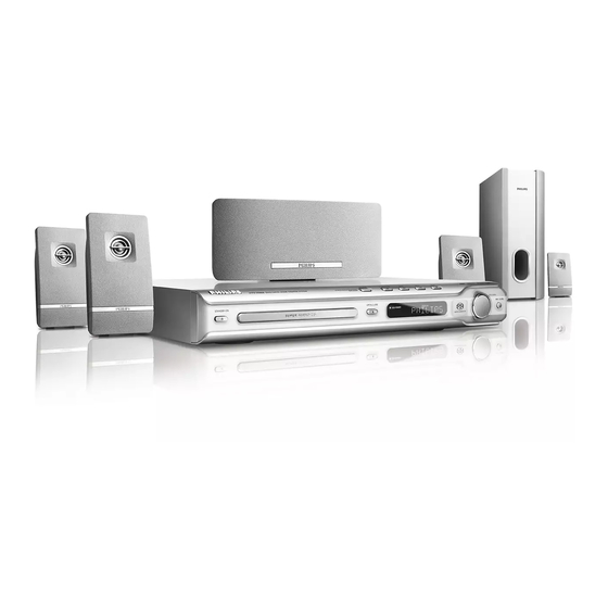
DVD Receiver
CLASS 1
Contents
1
2
3
4
5
6
7
© Copyright 2005 Philips Consumer Electronics B.V. Eindhoven, The Netherlands.
All rights reserved. No part of this publication may be reproduced, stored in
a retrieval system or transmitted, in any form or by any means, electronic,
mechanical, photocopying, or otherwise without the prior permission of Philips.
Published by KC-TE 0519 AV Systems
Version 1.1
Contents
Page
8
2
4
8
10
12
13
14
15
15
16
17
18
19
20
21
22
23
24
25
26
27
28
29
30
Printed in the Netherlands
Exploded View & Spare Parts List
Spare Part List
Subject to modi fi cation
/
98/75/51/12/05
Page
31
31
32
EN 3139 785 31191
Advertisement
Table of Contents

Related Manuals for Philips HTS3500S 98


Summary of Contents for Philips HTS3500S 98
-
Page 1: Table Of Contents
Layout: Mono Board (Bottom View) PSU Circuit Diagram © Copyright 2005 Philips Consumer Electronics B.V. Eindhoven, The Netherlands. All rights reserved. No part of this publication may be reproduced, stored in a retrieval system or transmitted, in any form or by any means, electronic, mechanical, photocopying, or otherwise without the prior permission of Philips. - Page 2 EN 2 HTS3500S Technical Specifi cations and Connection Facilities LOCATION OF PC BOARDS VERSION VARIATIONS: HTS3300 HTS3500S Type /Versions: /98/75 Features & Progressive Scan Line-Out TV-In Aux-In Y/Pb/Pr (YUV) Component Video Output Coax CVBS S-Video Output SCART...
-
Page 3: Hts3500S
Technical Specifi cations and Connection Facilities HTS3500S EN 3 1. Specifi cations General: AMPLIFIER: Mains voltage : 230V for /05, /12, /51 Output power 120V/230V for /98,/75 Front : 100W RMS / channel Rear : 75W RMS / channel Mains frequency : 50/60Hz for /98,/75, Center : 100W RMS... -
Page 4: Measurements Setup, Service Aid & Lead Free Requirements
EN 4 HTS3500S Measurements Setup, Service Aid & Lead Free Requirements 2. Measurements Setup, Service Aid & Lead Free Requirements MEASUREMENT SETUP Tuner FM Bandpass LF Voltmeter 250Hz-15kHz e.g. PM2534 e.g. 7122 707 48001 RF Generator e.g. PM5326 S/N and distortion meter e.g. - Page 5 Measurements Setup, Service Aid & Lead Free Requirements HTS3500S EN 5 SERVICE AIDS Service Tools: Universal Torx driver holder ........4822 395 91019 Torx bit T10 150mm ..........4822 395 50456 Torx driver set T6 - T20 ......... 4822 395 50145 Torx driver T10 extended ........
-
Page 6: Laser Product
EN 6 HTS3500S Measurements Setup, Service Aid & Lead Free Requirements WAARSCHUWING WARNING Alle IC’s en vele andere halfgeleiders zijn All ICs and many other semi-conductors are gevoelig voor electrostatische ontladingen (ESD). susceptible to electrostatic discharges (ESD). Onzorgvuldig behandelen tijdens reparatie kan Careless handling during repair can reduce life de levensduur drastisch doen verminderen. -
Page 7: Lead Free Requirements
Due to lead-free technology some rules have to be respected by the workshop during a repair: • Use only lead-free solder alloy Philips SAC305 with order code 0622 149 00106. If lead-free solder-paste is required, please contact the manufacturer of your solder-equipment. -
Page 8: Dismantling Instructions & Service Positions
EN 8 HTS3500S Dismantling Instructions & Service Positions Dismantling of the Tuner Module, 3. Dismantling Instructions MONO Board, Front Board, PSU Module Dismantling of the DVD Loader 1) Loosen 1 screw A (see Figure 3-3) to remove the Tuner Module (pos 1040). 1) The tray can be manually open by inserting a minus screw drive and push the lever in the direction as shown 2) Loosen 9 screws B (see Figure 3-3) and 4 screws... - Page 9 Dismantling Instructions & Service Positions HTS3500S EN 9 3.3 Service Positions Front Board Thick Insulation Sheet Mono Board PSU Board DVD Loader Thick Insulation Sheet...
-
Page 10: Service Test Program
EN 10 HTS3500S Service Test Program Service Test Program To start service test program refers to Service Mode open the tray with remote control refers to Version or front panel key, while plugging xx refers to Software version number of BEA in the mains cord press 2, 5 8 on (counting up from 01 to 99) remote control, the tray will close... - Page 11 Service Test Program HTS3500S EN 11 4.1.1 Reprogramming of DVD version Matrix Note: ISO9660 is mandatory, UDF discs are not supported! After repair, the customer setting and region code may be lost. The fi nal CDROM must not contain any other data except Reprogramming will put the set back in the state in which it has left the fi...
-
Page 12: Ftd Display Pin Connection
EN 12 HTS3500S FTD Display Pin Connection FTD Display Pin Connection... -
Page 13: Block Diagram
HTS3500S EN 13 Block Diagram, Wiring Diagram Block Diagram LINE SURR TV IN FRONT FRONT SUB_ SURR CENTER LEFT LEFT RIGHT RIGHT WOOFER 1501 1502 7662 +9.1V AM / FM SAA6581T RDS_Mux Tuner TM10 RIGHT RDS IC 2422 542 00014 LEFT RDS_CK RDS_DA... -
Page 14: Wiring Diagram
Block Diagram, Wiring Diagram HTS3500S EN 14 Wiring Diagram 8001 313911103781(FFC FOIL 10P/120/10P AD FOLD) Port-s SCART TU_SCL TU_SDA 1800 1802 1806 1502 1501 1401 1400 TU_SD 2P EH TO FAN TU_L TUNER TU_Stereo TM10 TU_R NC/RDS Mono board( AV+MPEG+AMP) 3139 243 31471 141X382 FR4 2-layer 11P FFC TO TUNER 10P EH TO PSU... -
Page 15: Circuit Diagram And Pwb Layout
HTS3500S EN 15 Circuit Diagram and PWB Layout Front: Display 1701 B12 6720 I9 1702 F2 7701 H2 1703 E2 7702-1 B5 1705 G4 7702-2 B6 1707 D2 7703 C4 1708 G8 7704 E5 FRONT DISPLAY 1709 B2 7705 I12 1710 H6 7706 I12 1711 H7... -
Page 16: Front: Display (Topview)
Circuit Diagram and PWB Layout HTS3500S EN 16 Front: Display (topview) 3139 113 35764_top.pdf_051305... -
Page 17: Front: Display (Bottom View)
HTS3500S EN 17 Circuit Diagram and PWB Layout Front: Display (Bottom view) 3139 113 35764_bottom.pdf_051305... -
Page 18: Front: Standby
Circuit Diagram and PWB Layout HTS3500S EN 18 Front: Standby 1900 A1 1901 A1 2901 B1 2902 B1 F901 A1 F902 A1 1901 1900 F901 F902 SKQNAB B2B-EH-A 3139 113 35774_bottom.pdf_051305 3139 113 35774_sem.pdf_051305 3139 113 35774_top.pdf_051305... -
Page 19: Mono Board: Circuit Diagram (Part 1)
HTS3500S EN 19 Circuit Diagram and PWB Layout Mono Board: Circuit Diagram (Part 1) 1101 D1 2219 I2 5120 B5 1102 G1 2220 E6 5122 C2 1103 H1 2221 E5 5123 D2 1105 I9 2222 F6 5124 D4 1107 F5 2223 G4 5125 D3 +S_V33... -
Page 20: Mono Board: Circuit Diagram (Part 2)
Circuit Diagram and PWB Layout HTS3500S EN 20 Mono Board: Circuit Diagram (Part 2) 2252 A4 2253 C4 2254 C4 2255 C4 2256 C4 2257 C4 2258 C4 2259 D10 2260 D11 3200 2261 D10 RDS_DAT RDS_DAT 2262 D10 2263 D11 RDS_CLK 2264 D7 RDS_CLK... -
Page 21: Mono Board: Circuit Diagram (Part 3)
HTS3500S EN 21 Circuit Diagram and PWB Layout Mono Board: Circuit Diagram (Part 3) 1300 B9 7305 D5 1301 D9 7306 C10 1302 G2 7307 E5 1305 D9 7308 E9 2301 B8 7309 G12 2302 B10 7310 G12 2303 B8 F301 C13 2304 B12 F303 G4... -
Page 22: Mono Board: Circuit Diagram (Part 4)
HTS3500S EN 22 Mono Board: Circuit Diagram (Part 4) 1401 G9 F405 E8 1402 C9 F406 E8 1403 F9 F407 E8 2106 1404 D9 F409 H8 2314 H6 F410 I7 2400 A5 F411 I7 2104 2107 2401 A5 F415 B2 100n 100n 2402 A5... -
Page 23: Mono Board: Circuit Diagram (Part 5)
HTS3500S EN 23 Circuit Diagram and PWB Layout Mono Board: Circuit Diagram (Part 5) 1500 D1 1501 H1 1502 F1 1506 G1 2500 A7 2501 A9 2502 C2 2504 C6 2520 2505 A2 2522 100p 2506 F6 F502 3500 100p 2507 G3 GND_tu 3501... -
Page 24: Mono Board: Circuit Diagram (Part 6)
Circuit Diagram and PWB Layout HTS3500S EN 24 Mono Board: Circuit Diagram (Part 6) 2110 I12 4602 A4 2601 C3 5604 A7 2602 C4 5605 G5 2603 I8 5606 I5 2610 H10 7613-1 B13 2614 B13 7613-2 C13 2615 B6 7615 A5 2616 B13 7616-1 D13... -
Page 25: Mono Board: Circuit Diagram(Part 7)
HTS3500S EN 25 Circuit Diagram and PWB Layout Mono Board: Circuit Diagram(Part 7) 2701 E4 T713 I8 2702 F5 T714 I9 2703 F1 2704 F2 2705 F3 2706 F3 2707 F4 2712 3752 T703 FE_Left 2712 A8 FE_Left 2713 A8 680R 2714 B8 2713... -
Page 26: Mono Board: Circuit Diagram (Part 8)
Circuit Diagram and PWB Layout HTS3500S EN 26 Mono Board: Circuit Diagram (Part 8) 1800 B12 1802-A E12 1802-B F12 1802-C G12 1806 G12 1807 H12 2803 B2 2815 C13 2816 C13 2817 C13 For Scart version only 2818 D13 2819 D11 T816 2823 E11... -
Page 27: Mono Board: Circuit Diagram (Part 9)
HTS3500S EN 27 Circuit Diagram and PWB Layout Mono Board: Circuit Diagram (Part 9) 1900 A1 1901 D2 2900 D4 2902 B5 2911 A1 2912 B1 2913 A2 7901 2913 2914 B3 LD1117DT 2916 B3 F900 100p T903 2918 C3 +3V3 +3V3 +1V8... -
Page 28: Layout: Mono Board (Topview)
Circuit Diagram and PWB Layout HTS3500S EN 28 Layout: Mono Board (Topview) Mono_3500_98_top.pdf_051305... -
Page 29: Layout: Mono Board (Bottom View)
HTS3500S EN 29 Circuit Diagram and PWB Layout Layout: Mono Board (Bottom view) Mono_3500_98_bottom.pdf_051305... -
Page 30: Psu Circuit Diagram
Circuit Diagram and PWB Layout HTS3500S EN 30 PSU Circuit Diagram (For information only) PSU 04-01-Circuit Diagram 1702 04.11.01.pdf_052005... -
Page 31: Technical Specifi Cations And Connection
Exploded View & Spare Parts List HTS3500S EN 31 Exploded View of the Set Figure 9-1... - Page 32 EN 32 HTS3500S Exploded View & Spare Parts List MISCELLANEOUS HTS3500S (05/12/51) RESISTORS 4822 466 11453 L7 MAIN SCORD BLOCK L7L 3210 4822 117 12662 10R X4 5% 4822 321 11499 MAINSCORD 2.0M - EU 3211 4822 117 12662 10R X4 5% 4822 321 11139 POWER CORD 3212 4822 117 12662...
- Page 33 Exploded View & Spare Parts List HTS3500S EN 33 DIODES FRONT BOARD HTS3500S (05/12/51) MISCELLANOUS 6726 4822 130 11397 BAS316 6727 4822 130 11397 BAS316 1701 3139 111 04131 FTD HUV-08SS57T (LX-3900SA) 6728 4822 130 11397 BAS316 1705 2422 129 16836 ROT ENCODER 12P EVEGC2F2012B B 1710 4822 276 13775 SWITCH...
- Page 34 Exploded View & Spare Parts List EN 34 HTS3500S MISCELLANEOUS HTS3500S (98/75) RESISTORS 4822 466 11453 L7 MAIN SCORD BLOCK L7L 3210 4822 117 12662 10R X4 5% 4822 321 11499 MAINSCORD 2.0M - EU 3211 4822 117 12662 10R X4 5% 4822 321 11139 POWER CORD 3212 4822 117 12662...
- Page 35 Exploded View & Spare Parts List HTS3500S EN 35 DIODES FRONT BOARD HTS3500S (98/75) MISCELLANOUS 6726 4822 130 11397 BAS316 6727 4822 130 11397 BAS316 1701 3139 111 04131 FTD HUV-08SS57T (LX-3900SA) 6728 4822 130 11397 BAS316 1705 2422 129 16836 ROT ENCODER 12P EVEGC2F2012B B 1709 2422 026 05691 SOC PHONE H 1P F 3.5...
- Page 36 11 REVISION LIST 11.1 Manual 3139 785 31191 1.Additional of HTS3500S/75 2.Replace of schematic diagram (point 4) in page 22 of document. 3.Additional of HTS3500S/75 for Reprogramming of DVD version Matrix in page 11 of documents. 4.Revise of spare parts list for HTS3500S/75...