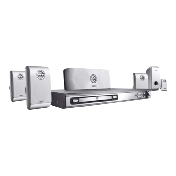
Philips HTS3410D/55 Service Manual
Philips hts3410d/55 dvd receiver service manual
Hide thumbs
Also See for HTS3410D/55:
- User manual (36 pages) ,
- Quick use manual (4 pages) ,
- Service manual (39 pages)
Table of Contents
Advertisement
Quick Links
DVD Receiver
Service
Service
Service
Service
Service
Service Manual
Copyright 2005 Philips Consumer Electronics B.V. Eindhoven, The Netherlands
©
All rights reserved. No part of this publication may be reproduced, stored in a retrieval system or
transmitted, in any form or by any means, electronic, mechanical, photocopying, or otherwise
without the prior permission of Philips.
Published by KC-ET0409 Service Audio Printed in The Netherlands Subject to modification.
Version 1.0
TABLE OF CONTENTS
Location of PC Boards ................................................ 1-2
Versions Variation ...................................................... 1-2
Specifications .............................................................. 1-3
Measurement Setup ................................................... 1-4
Service Aids ................................................................ 1-5
ESD & Safety Instruction ............................................ 1-6
Information about lead-free soldering ......................... 1-7
Setting Procedure & Repair Instructions ....................... 2
Disassembly Instructions & Service positions .............. 3
Block & Wiring Diagram ................................................ 4
Control / Power Switch / Volume Board ........................ 5
Tuner Board ................................................................... 6
DVD loader .................................................................... 7
Main Board .................................................................... 8
Power Board .................................................................. 9
Exploded View ............................................................. 10
HTS3410 D
Page
CLASS 1
LASER PRODUCT
GB
/55
3139 785 31390
Advertisement
Table of Contents

Related Manuals for Philips HTS3410D/55


Summary of Contents for Philips HTS3410D/55
- Page 1 Exploded View ............. 10 CLASS 1 LASER PRODUCT Copyright 2005 Philips Consumer Electronics B.V. Eindhoven, The Netherlands © All rights reserved. No part of this publication may be reproduced, stored in a retrieval system or transmitted, in any form or by any means, electronic, mechanical, photocopying, or otherwise without the prior permission of Philips.
- Page 2 System, Region code, Tuner, etc. setting procedure 5. Video Out Change 3) Region code change timer reset a) Press "SYSTEM" on R/C button Press below key to reset the timer : Hence in total, reprograming will be done by way of the 1) System Reset b) Select the menu using the "...
- Page 3 REPAIR INSTRUCTIONS (1 of 2)
- Page 4 REPAIR INSTRUCTIONS (2 of 2)
-
Page 5: Location Of Pc Boards
LOCATION OF PC BOARDS VERSION VARIATION: Type /Versions: HTS3410D Features & Board in used: / 55 Rotary Encoder (volume control) Aux Input Digital Output Line Output Progressive scan Power supply (110-127/220-240V) -
Page 6: Specifications
Frequency Response ....4 Hz - 20 kHz (44.1kHz) ............4 Hz - 22 kHz (48kHz) ............4 Hz - 44 KHz (96KHz) Digital Output ..................SPDIF (Sony Philips digital interface) Coaxial - PCM ..............IEC 60958 - Dolby Digital ......... IEC 60958, IEC 61937... -
Page 7: Measurement Setup
MEASUREMENT SETUP Tuner FM Bandpass LF Voltmeter 250Hz-15kHz e.g. PM2534 e.g. 7122 707 48001 RF Generator e.g. PM5326 S/N and distortion meter e.g. Sound Technology ST1700B Use a bandpass filter to eliminate hum (50Hz, 100Hz) and disturbance from the pilottone (19kHz, 38kHz). Tuner AM (MW,LW) Bandpass LF Voltmeter... - Page 8 SERVICE AIDS Service Tools: Universal Torx driver holder .........4822 395 91019 Torx bit T10 150mm ...........4822 395 50456 Torx driver set T6-T20 .........4822 395 50145 Torx driver T10 extended ........4822 395 50423 Compact Disc: SBC426/426A Test disc 5 + 5A ......4822 397 30096 SBC442 Audio Burn-in test disc 1kHz ....4822 397 30155 SBC429 Audio Signals disc .........4822 397 30184 Dolby Pro-logic Test Disc ........4822 395 10216...
- Page 9 WAARSCHUWING WARNING Alle IC’s en vele andere halfgeleiders zijn All ICs and many other semi-conductors are gevoelig voor electrostatische ontladingen susceptible to electrostatic discharges (ESD). (ESD). Careless handling during repair can reduce life Onzorgvuldig behandelen tijdens reparatie kan drastically. de levensduur drastisch doen verminderen. When repairing, make sure that you are Zorg ervoor dat u tijdens reparatie via een connected with the same potential as the mass...
- Page 10 You will find this and more technical information • Use only lead-free solder alloy Philips SAC305 with within the “magazine”, chapter “workshop news”. order code 0622 149 00106. If lead-free solder-paste is required, please contact the manufacturer of your For additional questions please contact your local solder-equipment.
-
Page 11: Disassembly Instructions
DISASSEMBLY INSTRUCTIONS Dismantling of the DVD Module 1) Loosen 4 screws "A" to remove the DVD Module as shown in figure 4. Dismantling of the Front Panel Assembly 1) Open the DVD Tray by using the Open/Close Button 2) Return the set to its upright position and remove the Tray while the Set is ON and disconnect the mains supply after Cover as shown in Figure 3 and close the tray manually removing the Tray Cover. - Page 12 SERVICE POSITIONS Dismantling of the Main PCB 1) Loosen 10 screw " D " at the back panel as shown in figure Service position A 2) Loosen 6 screw " E " on the top of main board as shown in figure 8.
- Page 13 BLOCK DIAGRAM...
- Page 14 WIRING DIAGRAM...
- Page 15 FTD DISPLAY PIN ASSIGNMENT CONTROL/POWER SWITCH BOARD /VOLUME (2G - 10G) TABLE OF CONTENTS FTD Display Pin Assignment ........... 5-1 Pin Connection ..............5-1 Circuit Diagram ..............5-2 PCB Layout Top View ............5-3 PCB Layout Bottom View ..........5-3 Electrical Parts List &...
- Page 16 CIRCUIT DIAGRAM - KEY BOARD C2201 R2251 C2202 R2252 C2204 R2253 C2206 R2254 C2207 R2255 C2208 RB201 C2209 RB202 C2212 RB202A C2213 RB202B C2214 RB203A C2215 RB203B C2216 SN2201 C2217 TA2201 C2218 TA2202 C2219 TA2203 C2220 TA2204 C2221 TA2205 C2222 TA2206 C2223 TA2207...
- Page 17 PCB LAYOUT - KEY BOARD (TOP) C2204 D2201 RB202 TA2201 TA2207 C2207 D2202 RB202A TA2202 TA2208 C2208 DP2201 RB202B TA2203 VR2201 C2213 LD2201 RB203A TA2204 XL2201 C2217 R2228 RB203B TA2205 ZD2201 C2223 RB201 SN2201 TA2206 PCB LAYOUT - KEY BOARD (BOTTOM) C2201 C2219 R2227...
- Page 18 ELECTRICAL PARTLIST - KEY (CONTROL , VOLUME , PWR ) PCBA MISCELLANOUS IC2201 9965 000 23592 IC 18PIN HT48R05A-1 SOP HOLTEK LD2201 9965 000 26953 LED 3 DIA RED ROUND HP TA2201 9965 000 26950 AI TACT SW SKHVBE3520 ALPS TA2202 9965 000 26950 AI TACT SW SKHVBE3520 ALPS TA2203 9965 000 26950 AI TACT SW SKHVBE3520 ALPS TA2204 9965 000 26950 AI TACT SW SKHVBE3520 ALPS...
-
Page 19: Tuner Board
TUNER ADJUSTMENT TABLE Waverange Input frequency Input Tuned to Adjust Output Scope/Voltmeter VARICAP ALIGNMENT 108MHz 6.5V ±1.2V check 87.5 - 108MHz (50kHz grid) 87.5MHz check 1.0V ±0.5V 1602KHz check 7.8V ± 0.2V T005 1.1V ± 0.5V 531KHz 530-1710kHz (10kHz grid) TUNER BOARD ( 21L / 21L / 37S ) check... - Page 20 CIRCUIT DIAGRAM - TUNER BOARD ANT001 A1 R004 C002 R005 C005 R006 C007 R010 C006 R011 C008 R015 C009 R016 R017 R018 R019 C010 R020 C011 R021 C012 R023 C013 R024 C014 R025 C015 R026 C016 R027 C019 R028 C020 R029 C021 R030...
- Page 21 PCB LAYOUT - TUNER BOARD (TOP) ANT001 C025 D002 IF003 JWP8 T001 VD001 C005 C030 D003 JWP2 JWP9 T002 VD002 C006 C035 D004 JWP3 T003 VD003 C007 C047 D005 JWP4 L001 T005 VD004 C009 CN001 IC001 JWP5 Q001 T006 VR001 C019 CN002 IF001...
- Page 22 PCB LAYOUT - TUNER BOARD (BOTTOM) C013 C023 C037 C048 R005 R019 R028 C014 C026 C038 C050 R006 R020 R029 C001 C015 C029 C039 C052 R007 R021 R030 C002 C016 C031 C040 IC001 R010 R023 R031 C008 C020 C032 C041 Q003 R011 R024...
- Page 23 9965 000 27096 COND DISC 100PF 50V 5% NPO Q003 9940 000 00921 XISTR PNP 2SA812 HFE:200-400 IC001 9965 000 27003 IC 44 PIN TEA5757H QFP44 PHILIPS Q003 9965 000 27004 XISTR PNP BF550 SOT23 PHILIPS IF001 9965 000 24093 CERFILTER 3P 10.7MHZ LT10.7MA5 IF002 9965 000 24670 CER FILTER 10.7 MHZ...
-
Page 24: Dvd Loader
DVD LOADER It is not recommended for component repair on this Module but to replace the major assembly when it becomes defective. Therefore limited service parts list are published in this chapter. TABLE OF CONTENTS Explorer View (DVD Loader) ........... 7-2... - Page 25 Explorer view...
-
Page 26: Main Board
ES6629F INTERNAL IC DIAGRAM DVD/CD Mot o r OP U Motor Dr i v er ES6 603 V i deo T V Di splay RF Amp SDRA M Au dio DAC Spe akers 8/16-MB Au dio ADC E S 6629 M i c r o phon e I n V i bratto-II MAIN BOARD... - Page 27 VOLTAGES IC201 (ES6629F) IC405 (M62446AFP) PIN NO 1 PIN NO 1 Voltage 3.3 1.77 1.77 1.77 Voltage PIN NO 21 PIN NO 21 Voltage 3.3 2.8 3.1 0.2 3.3 1.3 1.3 3.3 1.4 1.3 1.3 1.2 1.3 Voltage PIN NO 41 PIN NO 41 Voltage Voltage...
- Page 28 CIRCUIT DIAGRAM (1)- MAIN BOARD C267 R824 C2001 C862 R212 C268 C863 R213 R825 C2002 C269 C864 R214 R826 C2003 R827 C2004 C270 C865 R215 C271 C866 R216 R828 C2005 R829 C2006 C272 C867 R217 C273 C868 R218 R830 C2007 C274 C869 R219...
- Page 29 CIRCUIT DIAGRAM (2)- MAIN BOARD C475 R436 R528 C5112 C966 L952 C476 C5113 C967 L955 R437 R529 C477 C5114 C968 L957 R438 R530 C478 R439 R531 C5115 C969 L958 C479 C5116 C970 R440 R532 C480 C5117 C971 R441 R533 C481 C5118 C972 R442...
- Page 30 PCB LAYOUT - MAIN BOARD (TOP) C413 C475 C5066 C808 C841 FB5004 IC502 Q405 R471 R5008 R837 RN204 ZD802 C211 C266 C445 C5005 C576 C965 L504 R227 R414 R442 R563 R808 R884 IC503 C212 C268 C351 C414 C446 C476 C5006 C507 C531 C577...
- Page 31 PCB LAYOUT - MAIN BOARD (BOTTOM) C2004 C2030 C223 C291 C5051 C5093 C5111 C524 C594 C865 D504 L803 Q410 R5047 R532 C2032 C224 C250 C5052 C5112 C525 C596 D505 Q411 R354 C2005 C5094 C866 L804 R5048 R533 C2006 C2033 C225 C251 C5059 C5095...
- Page 32 ELECTRICAL PARTLIST - MAIN BOARD MISCELLANOUS CAPACITORS C511 9965 000 26917 CHIP CAP 0.1UF/100V X7R /- 0.1 L208 9965 000 26926 CHIP INDUC 1 UH 0.1 D310 9965 000 19409 DIODE CHIP BAV16W/IN4148W CF5041 9965 000 23595 RES 2P 600KHZ ORANGE BOX TYPE C512 9965 000 26917 CHIP CAP 0.1UF/100V X7R /- 0.1 D311...
- Page 33 9940 000 00846 IC 24PIN TDA8920BTH service spare parts. RN204 9965 000 23613 CHIP ARRAY 4X4.7KOHM 1/16W 5% IC504 9965 000 27092 IC 14 PIN 74HCU04D PHILIPS TS RN205 9965 000 23614 CHIP ARRAY 10 OHMX4 1/16 W 5% IC505 5322 209 14477 HEF4013BT...
- Page 34 POWER + RGB + PHONE BOARD TABLE OF CONTENTS Circuit Diagram ..............9-2 PCB Layout ............... 9-3 Electrical Parts List ............9-4...
-
Page 35: Power Board
CIRCUIT DIAGRAM - POWER BOARD BD901 D906 R954 C901 D907 R955 L-45UH-8A JMP-100 IS 1/4W R04-1-F IS 1/4W 1 OHMRES FUSE 100U 35V C902 D910 R956 SCREW-A SCREW-A C955 C104P-100V 470P-1KV JMP18 C965 C104P-100V CN903 IS 1/6W R06-10KM IS 1/6W 10KOHM 1% L952 C903 D951... - Page 36 PCB LAYOUT - POWER BOARD (/17) R970 GT905 BD901 IC901 R971 C901 R972 C902 IC902 R973 C903 IC951 R974 C904 IC952 R975 C905 IC953 R976 C906 JMP01 R977 JMP02 C907 R978 JMP03 C908 R979 JMP04 C909 R980 JMP05 C910 R981 JMP06 C911 R982...
- Page 37 ELECTRICAL PARTLIST - POWER PCBA MISCELLANOUS DIODES Q951 9965 000 26946 XISTR PNP 2SB772P/Q NEC BD901 9940 000 00931 BRIDGE KBU808 8A 1000V C956 9940 000 00936 COND DISC 470PF 1KV 10% D903 9965 000 26949 DIODE SW 1N4148 PB<1000PPM Q952 9965 000 26946 XISTR PNP 2SB772P/Q NEC L901...
-
Page 38: Exploded View
10-1 10-1 MECHANICAL EXPLODED VIEW... - Page 39 10-2 10-2 MECHANICAL & ACCESSORIES PARTS LIST - MAIN UNIT SUBWOOFER ASSEMBLY BREAKDOWN MISCELLANEOUS 9965 000 29275 FRAME A’SSY 9965 000 29291 DVD LOADER ME L2HR3402 9965 000 29276 CLOTH FRAME 9965 000 23639 VOLUME KNOB ABS 9965 000 29277 CLOTH 9965 000 29307 FRONT PANEL HIPS 94HB 9965 000 29278 PLASTIC FOOT 9965 000 23640 VOLUME DOCKING ABS...