Advertisement
SERVICE MANUAL
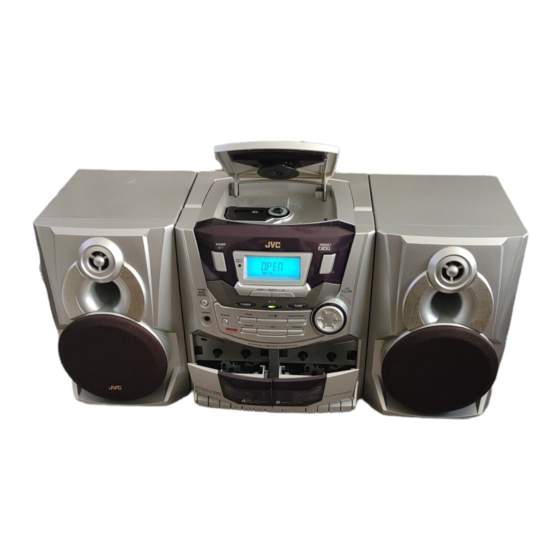
CD PORTABLE COMPONENT SYSTEM
Unit No
SP-PCX250
Contents
Safety precaution ------------------ 2
Disassembly method -------------- 4
Adjustment method ---------------- 6
TOC read ---------------------------- 10
Major IC Description -------------- 11
PC-X250
Unit No
CA-PCX250
COPYRIGHT © 2001 VICTOR COMPANY OF JAPAN,LTD (By JCA)
Unit No
SP-PCX250
Area Suffix
J ---- USA
C ---- Canada
Block/Wiring Diagram ------------------ 25
Circuit Diagram -------------------------- 27
PCB drawing ----------------------------- 29
Assembly ---------------------------------- 32
Packing ------------------------------------ 42
PC-X250
No. 28001
Oct. 2001
Advertisement

Related Manuals for JVC PC-X250


Summary of Contents for JVC PC-X250
-
Page 1: Table Of Contents
PC-X250 SERVICE MANUAL CD PORTABLE COMPONENT SYSTEM PC-X250 Unit No Unit No Unit No SP-PCX250 CA-PCX250 SP-PCX250 Area Suffix J ---- USA C ---- Canada Contents Safety precaution ------------------ 2 Block/Wiring Diagram ------------------ 25 Disassembly method -------------- 4 Circuit Diagram -------------------------- 27... -
Page 2: Safety Precaution
PC-X250 Safety Precautions 1. This design of this product contains special hardware and many circuits and components specially for safety purposes. For continued protection, no changes should be made ti the original design unless authorised in writing by the manufacturer. Replacement parts must be identical to those used in the original circuits. -
Page 3: Preventing Static Electricity
PC-X250 Preventing static electricity Electrostatic discharge (ESD), which occurs when static electricity stored in the body, fabric, etc. is discharged, can destroy the laser diode in the traverse unit (optical pcikup). Take care to prevent this when performing repairs. 1.1. Grounding to prevent damage by static electricity Static electricity in the work area can destroy the optical pickup (laser diode) in devicessuch as DVD players. -
Page 4: Disassembly Method
PC-X250 Disassembly method Removing the rear panel 1. From behind the body, remove the Five screws A retaining the rear panel. 2. Then remove the Two screws B retaining the bottom of rear panel. 3. Take out the rear panel from the body. - Page 5 PC-X250 Removing the Audio Board 1.Open & remove the rear panel 2. Remove the Connector CN201, CN202, CN203, CN405, CN502, CN801 & CN301 on the Audio Board. 3. Remove the two Screws C retaining the Audio Board. CN202 Screw C...
-
Page 6: Adjustment Method
PC-X250 Adjustment method Measurement instruments required for Tuner section adjustment Low frequency oscillator Voltage applied to tuner ---------- +B:DC 4.9V This oscillator should have a capacity to output VT:DC 12V 0dBs to 600 at an oscillation frequency of Reference measurement ----- 26.1mV(0.28V)/3... - Page 7 PC-X250 TAPE DECK ADJUSTMENTS HEAD AZIMUTH ADJUSTMET ( 1 ) Load the test tape TCC-182A 8KHz for azimuth adjustment. ( 2 ) Press the PLAY button. ( 3 ) Use a cross-tip screwdriver to turn the screw for azimuth adjustment so that the left and right output are maximized...
- Page 8 PC-X250 Tape recorder section Measurement Standard Adjusting] Items Measrrnment methed conditions Values positions Confirmation Test tape 1 Playback the test tape TCC-182A (8KHz) Maximum Adjust the head of head angle :TA-182A(8KHz) 2 With the recording & playback mechanism, output azimuth screw...
- Page 9 PC-X250 Electrical Performance Measurement Standard Adjusting ITEMS Measrrnment methed conditions Values positions Adjustment of Mode:Forward or 1 With the recording and playback recording bias reverse mode mechanism, load thd test tapes current Recording mode TDK-60 , and set the mechanism to the recording 4.5 A...
-
Page 10: Toc Read
PC-X250 Flow of functional operation until TOC read Check Point Power ON Power Key Slider turns REST Check that the voltage at the pin SW ON. 16 of IC903 is OV (a moument)? Automatic tuning of TE offset Laser ON... -
Page 11: Major Ic Description
PC-X250 Description of major ICs LC587008 System Block Diagram for the LC587008, LC587006 and LC587004 RAM: Data memory Instruction register ROM: Program memory STS1: Status register 1 Data pointer register STS2: Status register 2 BNK: Bank register STS3: Status register 3... - Page 12 PC-X250 LC72131 Block Diagram 1 - 12...
- Page 13 PC-X250 LC72131 Pin Functions Pin No. Symbol (MFP pin Nos. are Type Functions Circuit configuration in parentheses.) 1 (1) ¥ Crystal resonator connection Xtal OSC XOUT 22 (20) (4.5/7.2 MHz) ¥ FMIN is selected when the serial data input DVS bit is set to 1.
- Page 14 PC-X250 LC72131 Pin Functions Pin No. Symbol (MFP pin Nos. are Type Functions Circuit configuration in parentheses.) 21 (19) Ground ¥ The LC72131 ground Ñ ¥ Dedicated output pins ¥ The output states are determined by BO1 to BO4 bits in the serial data.
-
Page 15: Top View
PC-X250 LC75342 Pin Assignment VREF TEST LOUT ROUT LBASS2 RBASS2 LBASS1 RBASS1 LC75342 LTRE RTRE LSELO RSELO TOP VIEW LC75342 Pin Functions. Pin No. Description Notes ¥ Connection to the 0.5 ´ V voltage generator circuit used as the analog signal ground. - Page 16 PC-X250 LC75342 Pin Functions Pin No. Description Notes ¥ Input signal connections LSEL0 ¥ Input selector outputs RSEL0 LBASS1 LBASS2 ¥ Connections for the resistors and capacitors that form the bass band filters. RBASS1 RBASS2 ¥ Volume control and equalizer input LOUT ¥...
- Page 17 PC-X250 LC78622 Pin Assignment LC78622 Pin Function Pin No. Symbol Function SBCK Subcode readout clock input. This is a Schmitt input. (Must be connected to 0 V when unused.) Output for the 7.35 kHz synchronization signal divided from the crystal oscillator Subcode Q output standby output Read/write control input.
- Page 18 PC-X250 LC78622 Pin Functions Pin No. Symbol Function DEFI Defect detection signal (DEF) input. (Must be connected to 0 V when unused.) Test input. A pull-down resistor is built in. Must be connected to 0 V. External VCO control phase comparator output Ð...
- Page 19 PC-X250 LA6541D Pin Assignment Level Shift Level Shift Level Shift Level Shift Regulator 1 - 19...
- Page 20 PC-X250 LA6541D Pin Functions Pin No. Pin Name Description (Function) Power supply (shorted with pin 30) Mute ON/OFF control for all BTL AMP outputs BTL AMP 1 input BTL AMP 1 input (for gain control) BTL AMP 1 output (non-inverting side)
- Page 21 PC-X250 LA9241M Equivalent Circuit Block Diagram Microcontroller INTERFACE 1 - 21...
- Page 22 PC-X250 LA9241 Pin Functions Symbol Contents FIN2 Pickup photodiode connection pin. Added to FIN1 pin to generate the RF signal, subtracted from FIN1 pin to generate the FE signal. FIN1 Pickup photodiode connection pin. Pickup photodiode connection pin. Subtracted from F pin to generate the TE signal.
- Page 23 PC-X250 BA3126 Block Diagram BA3308 Block Diagram 1 - 23...
- Page 24 PC-X250 BA3416BL Block Diagram 1 - 24...