Vertex Standard VXR-7000 Service Manual
(vhf) desktop repeater
Hide thumbs
Also See for VXR-7000:
- Service manual (146 pages) ,
- Operating manual (44 pages) ,
- Alignment manual (4 pages)
Table of Contents
Advertisement
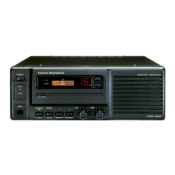
Desktop Repeater
VXR-7000
Service Manual
©2003 VERTEX STANDARD CO., LTD.
This manual provides technical information necessary for servicing the VXR-7000 FM Land Mobile Repeater.
Servicing this equipment requires expertise in handling surface-mount chip components. Attempts by non-qualified
persons to service this equipment may result in permanent damage not covered by the warranty, and may be illegal in
some countries.
Two PCB layout diagrams are provided for each double-sided circuit board in the repeater. Each side of is referred to
by the type of the majority of components installed on that side ("leaded" or "chip-only"). In most cases one side has only
chip components, and the other has either a mixture of both chip and leaded components (trimmers, coils, electrolytic
capacitors, ICs, etc.), or leaded components only.
While we believe the technical information in this manual to be correct, VERTEX STANDARD assumes no liability
for damage that may occur as a result of typographical or other errors that may be present. Your cooperation in pointing
out any inconsistencies in the technical information would be appreciated.
Operating Manual Reprint ............................ 2
CE27 Programming Software Instruction ............................. 9
Specifications ................................................. 14
Exploded View & Miscellaneous Parts .... 15
Block Diagram ............................................... 17
Interconnection Diagram ............................. 20
Circuit Description ...................................... 21
Alignment ....................................................... 23
(VHF)
E136790A
Contents
VERTEX STANDARD CO., LTD.
4-8-8 Nakameguro, Meguro-Ku, Tokyo 153-8644, Japan
VERTEX STANDARD
US Headquarters
10900 Walker Street, Cypress, CA 90630, U.S.A.
YAESU EUROPE B.V.
P.O. Box 75525, 1118 ZN Schiphol, The Netherlands
YAESU UK LTD.
Unit 12, Sun Valley Business Park, Winnall Close
Winchester, Hampshire, SO23 0LB, U.K.
VERTEX STANDARD HK LTD.
Unit 5, 20/F., Seaview Centre, 139-141 Hoi Bun Road,
Kwun Tong, Kowloon, Hong Kong
Board Unit (Schematics, Layouts & Parts)
Pa Unit .................................................................... 27
Tx Unit ..................................................................... 35
Rx Unit .................................................................... 43
Cntl Unit ............................................................... 55
Lpf Unit ................................................................... 73
Display Unit ............................................................ 75
Key Unit ................................................................... 79
Filter Unit ................................................................ 87
Vr Unit .................................................................... 95
Sql Unit .................................................................. 97
Ps Unit ..................................................................... 99
1
Advertisement
Table of Contents

Related Manuals for Vertex Standard VXR-7000


Summary of Contents for Vertex Standard VXR-7000
- Page 1 ICs, etc.), or leaded components only. While we believe the technical information in this manual to be correct, VERTEX STANDARD assumes no liability for damage that may occur as a result of typographical or other errors that may be present. Your cooperation in pointing out any inconsistencies in the technical information would be appreciated.
-
Page 2: Operating Manual Reprint
BASE/REPEATER Switch as High/Low power selection, as determined by your This switch toggles the operating mode between the Vertex Standard dealer. The LED above it glows green “REPEATER” mode and the “BASE” transceiver when this function is activated. For further details, mode. - Page 3 This DB-25 connector provides a data interface be- When operating from AC mains, a small trickle cur- tween the microprocessor in the VXR-7000 and pe- rent is present at these terminals to maintain battery ripheral devices (such as the VX-TRUNK Unit).
- Page 4 ACC Connector Port Pin 7: GND Chassis ground for all logic levels and power supply The VXR-7000 repeater is provided with a 25-pin DB- return. 25F female connector for interconnections to accesso- ries. Use a DB-25M 25-pin male connector to connect Pin 8: RSSI [Analog Output] accessories to the repeater.
- Page 5 Operating Manual Reprint Pin 12: EXT PTT Pin 20: GND This input is internally pulled up to 5 VDC. When Chassis ground for all logic levels and power supply pulled low by an external device, it keys the repeater return. transmitter while the repeater is operating in the Pin 21: A-OUTPUT [Logic Output] (Active Low) “BASE”...
- Page 6 Operating Manual Reprint LINE Interface Port Installation The VXR-7000 is provided with an 8-pin modular jack Antenna Considerations for line interfacing applications. A Western Electric ® modu- Repeater operation without a duplexer requires that two lar-type RJ45 plug should be used to connect to this jack.
- Page 7 Operating Manual Reprint DC Power Supply Backup Equipment Location For uninterrupted operation during power failures, a 12 While the operating temperature range of the repeater is volt rechargeable type battery (55-Ah or more recom- quite broad, the best location is one in which the air tem- mended) may be connected to the BATT terminal posts perature does not approach the extremes of the specified on the rear panel.
- Page 8 Operating Manual Reprint Changing Switching Regulator unit AC Mains Jumper Wiring Referring to Figure 4, perform the correct jumper wir- Before attempting this jumper wire change, remove the ing on the Switching Regulator Unit for the AC Mains AC power cord from the AC jack on the rear panel. voltage used in your area (100-127 VAC or 207-253 VAC).
-
Page 9: Ce27 Programming Software Instruction
• CE27.HLP Before connecting the VXR-7000 for programming, turn Important Note! off both the computer and the VXR-7000. Now connect the VPL-1 Connection Cable to the computer’s serial port Do not run the CE27 programming software di- and the VXR-7000. - Page 10 When this parameter is set to “on,” this function causes quency using the [A ] key; RROW the VXR-7000 to send out a “blip” on the portable/mobile press [E ] again to accept the NTER radio is frequency each time the portable radio is unkeyed.
- Page 11 ULTI This parameter selects the desired power output from the ” window directly. ELECT VXR-7000 on the current channel. The available values CWID ANI/ENI: Select the Identifier mode are HIGH and LOW. ] bar to toggle the selections “CW ID,”...
- Page 12 Operating Manual Reprint 1. Connect the VXR-7000’s TX antenna port to a watt- Duplexer Installation meter and dummy load (the duplexer must not be con- nected at this point). Connect any Vertex Standard Important Note microphone to the MIC jack, and place the BASE/ Be certain to observe the specifications for Frequen- REPEATER switch in the “BASE”...
- Page 13 Operating Manual Reprint 7. If your repeater’s Tx/Rx frequency relationship is “up- Installations per shift” type (TXf > RXf), connect the coaxial cable 1. Remove the 14 screws affixing the top and bottom from the RX Unit to the LOW PASS jack of the du- covers of repeater, and remove the covers (Figure 1).
-
Page 14: Specifications
Specifications General Frequency Range: 136 ~ 150 MHz (A) or 150 ~ 174 MHz (C) Number of Channels: 12.5/25 kHz Channel Spacing: ±2.5 ppm Frequency Stability: 50 Ω (N-Type) Antenna Impedance: Tx Activation System: Carrier-operated, CTCSS tone operated, DCS operated, or remote control 115/230 V AC ±10%, 50/60 Hz or 13.8 VDC Power Requirements: Ambient Temperature Range: –30 °C ~ +60 °C... - Page 15 Exploded View & Miscellaneous Parts Ref. YAESU P/N Description Qty. U04308001 SEMS SCREW HSM3×8 U30312012 FLAT HEAD SCREW M3×12BSNI FILTER Unit RA0181300 U04408001 SEMS SCREW HSM4×8 TOP CASE U30306012 FLAT HEAD SCREW M3×6BSNI U30314012 FLAT HEAD SCREW M3×14BSNI U30308012 FLAT HEAD SCREW M3×8BSNI S8001786 U04306002 SEMS SCREW HSM3×6NI...
- Page 16 Exploded View & Miscellaneous Parts Note:...
-
Page 17: Block Diagram
Block Diagram... - Page 18 Block Diagram...
- Page 19 Block Diagram...
-
Page 20: Interconnection Diagram
Interconnection Diagram... -
Page 21: Circuit Description
Circuit Description Receive Signal Path audio amplifier Q4019-4 to J4008’s pin 10, providing the re- peater transmit audio. Incoming RF from the RX antenna jack is delivered to the RX Unit and passes through the protection diode D3001 A portion of the audio signal from the active high pass filter (MA143) and a varactor-tuned band pass filter consisting of section of Q4024 is de-emphasized by Q4020-1 (NJM2902M), coils L3002 and L3004, capacitors C3019, C3021, C3024,... - Page 22 Circuit Description ceiving frequency. The RX VCO output passes through buffer finally amplified by power amplifier Q1507 (2SC5125) up to amplifier Q3009 and first local amplifier Q3011 to the first mixer 50 Watts. Harmonic and spurious radiation in the final output D3014, as described previously.
-
Page 23: Alignment
Alignment The VXR-7000 is carefully aligned at the factory for Required Test Equipment the specified performance across the entire operating fre- RF Signal Generator with calibrated output level at 200 quency range. Realignment should therefore not be nec- essary except in the event of a component failure. All com-... - Page 24 Alignment Set up the test equipment as shown below, and apply Transmitter AC power to the repeater. Press the BASE/REPEATER switch on the front panel of the repeater so as to set it to the BASE mode if the The repeater must be programmed for use in the in- REPEATER LED is on.
- Page 25 Alignment Receiver Receiver parameters (excluding PLL) The following receiver parameters can be adjusted from PLL VCV (Varactor Control Voltage) Check the computer by utilizing the CE27 Channel/Alignment Connect the DC voltmeter between the VCV check Diskette. Refer to the onboard help of the CE27 Chan- point (on the RX Unit) and chassis ground.
- Page 26 Alignment Repeater Mode Base Mode Deviation Adjustment Alignment Setup First ensure that the “DUPLEX” mode of operation is Set the BASE/REPEATER switch on the front panel enabled via CE27 programming. of the repeater to the BASE mode (the REPEATER LED will turn off). Set the BASE/REPEATER switch on the front panel of the repeater to the “REPEATER”...
- Page 27 PA Unit Circuit Diagram...
- Page 28 PA Unit Parts Layout Side A 2SC5125 PF0314 (TYP C) (Q1507) PF0313 (TYP A: Lot. 7~) (Q1502)
- Page 29 PA Unit Side B TA75S01F (SA) NJM78L09UA (8H) UN5213 (8C) 2SB1122S (BE) 2SC3357 (RK) 2SC4116GR (LG) 1SS319 (A4) MA143 (MC) (Q1509) (Q1508) (Q1506) (Q1503, 1505) (Q1501) (Q1504) (D1503, 1504) (D1502) RN739F (5F) (D1501)
- Page 30 PA Unit Note:...
-
Page 31: Parts List
PA Unit Parts List DESCRIPTION VALUE MFR’S DESIG VXSTD P/N VERS LOT SIDE LAY ADR PCB with Components CS1645001 VERSION C CS1645002 VERSION A Printed Circuit Board FR003510C C 1501 CHIP CAP. 0.001uF GRM39B102K50PT K22174821 C 1503 CHIP CAP. 56pF GRM39CH560J50PT K22174229 C 1504 CHIP CAP. - Page 32 PA Unit REF. DESCRIPTION VALUE TOL. MFR’S DESIG VXSTD P/N VERS. LOT. SIDE LAY ADR C 1534 AL.ELECTRO.CAP. 1000uF RJ3-25V102M 1000UF K40149041 C 1534 AL.ELECTRO.CAP. 1000uF RJ3-25V102M 1000UF K40149041 C 1535 CHIP CAP. 0.001uF 500V GRM42-6W5R102K500PT K22271801 C 1536 CHIP CAP. 0.01uF 200V GRM42-6X7R103K200PT...
- Page 33 PA Unit REF. DESCRIPTION VALUE TOL. MFR’S DESIG VXSTD P/N VERS. LOT. SIDE LAY ADR D 1503 DIODE 1SS319 TE85R G2070080 D 1504 DIODE 1SS319 TE85R G2070080 FB1501 M.RFC FBA03VA450AB-00 L1190389 FB1502 FERRITE BEADS 4A2 RI3X3-1 L9190001 FB1503 FERRITE BEADS 4A2 RI3X3-1 L9190001 J 1501...
- Page 34 PA Unit REF. DESCRIPTION VALUE TOL. MFR’S DESIG VXSTD P/N VERS. LOT. SIDE LAY ADR R 1523 CHIP RES. 1/10W 5% RMC1/10T 103J J24205103 VERSION C R 1523 CHIP RES. 1/10W 5% RMC1/10T 103J J24205103 VERSION A R 1523 CHIP RES. 6.8k 1/10W 5% RMC1/10T 682J...
- Page 35 TX Unit (Lot. 1~) Circuit Diagram...
- Page 36 TX Unit (Lot. 1~) Parts Layout Side A Side B MB15A02PFV TA78L05F (AE) 2SK508 (K52) 2SC3357 (RK) UN5213 (8C) 2SA1179 (M6) 2SC4116GR (LG) UN5215 (8E) XN1213 (9L) RN739F (5F) MA143 (MC) (Q2001) (Q2012) (Q2005) (Q2010) (Q2014, 2016) (Q2013, 2017) (Q2002, 2006, 2009) (Q2004) (Q2011, 2015) (D2007, 2008)
- Page 37 TX Unit (Lot. 6~) Circuit Diagram...
- Page 38 TX Unit (Lot. 6~) Parts Layout Side A Side B MB15A02PFV TA78L05F (AE) 2SK508 (K52) 2SC3357 (RK) UN5213 (8C) 2SA1179 (M6) 2SC4116GR (LG) UN5215 (8E) XN1213 (9L) RN739F (5F) MA143 (MC) (Q2001) (Q2012) (Q2005) (Q2010) (Q2014, 2016) (Q2013, 2017) (Q2002, 2006, 2009) (Q2004) (Q2011, 2015) (D2007, 2008)
- Page 39 TX Unit Parts List DESCRIPTION VALUE MFR’S DESIG VXSTD P/N VERS LOT SIDE LAY ADR PCB with Components CB0740001 VERSION C CB0740002 VERSION A Printed Circuit Board FR003520D FR003520E C 2001 CHIP CAP. 0.001uF GRM39B102K50PT K22174821 C 2001 CHIP CAP. 0.033uF ECJ1VB1C333K K22129515...
- Page 40 TX Unit REF. DESCRIPTION VALUE TOL. MFR’S DESIG VXSTD P/N VERS. LOT. SIDE LAY ADR C 2055 CHIP CAP. 470pF GRM39CH471J50PT K22174249 C 2056 CHIP CAP. 0.001uF GRM39B102K50PT K22174821 C 2057 CHIP CAP. 0.001uF GRM39B102K50PT K22174821 C 2058 CHIP CAP. 0.001uF GRM39B102K50PT K22174821...
- Page 41 TX Unit REF. DESCRIPTION VALUE TOL. MFR’S DESIG VXSTD P/N VERS. LOT. SIDE LAY ADR R 2008 CHIP RES. 1/16W 5% RMC1/16 333JATP J24185333 R 2009 CHIP RES. 1/16W 5% RMC1/16 223JATP J24185223 R 2010 CHIP RES. 1/16W 5% RMC1/16 473JATP J24185473 R 2011 CHIP RES.
- Page 42 TX Unit REF. DESCRIPTION VALUE TOL. MFR’S DESIG VXSTD P/N VERS. LOT. SIDE LAY ADR R 2066 CHIP RES. 1/16W 1% RMC1/16 563FTP J24183563 R 2067 CHIP RES. 1/16W 1% RMC1/16 823FTP J24183823 R 2067 CHIP RES. 1/16W 5% RMC1/16 000JATP J24185000 R 2068 CHIP RES.
- Page 43 RX Unit (Lot. 1~) Circuit Diagram...
- Page 44 RX Unit (Lot. 1~) Parts Layout Side A MB15A02PFV TA31136FN GN2011-Q (4W) TA78L05F (AE) UN5215 (8E) 2SA1586Y (SY) 2SC2620 (QB) 2SK508 (K52) 2SC3357 (RK) MA143 (MC) (Q3001) (Q3012) (D3014) (Q3021) (Q3004) (Q3003) (Q3016) (Q3007) (Q3008, 3011) (D3011, 3018, 3019) 2SC4116GR (LG) RN739F (5F) (Q3002, 3014) (D3003)
- Page 45 RX Unit (Lot. 1~) Side B XN1213 (9L) 2SB1122S (BE) 2SA1586Y (SY) 2SC2812 (L6) MA143 (MC) MA142WK (MU) HZM5.6NB2 (562) (Q3015, 3020, 3022) (Q3013) (D3001, 3021) (D3015, 3016) (Q3018) (Q3006) (D3017) 2SC4116GR (LG) (Q3005, 3010)
- Page 46 RX Unit (Lot. 6~) Circuit Diagram...
- Page 47 RX Unit (Lot. 6~) Parts Layout Side A MB15A02PFV TA31136FN GN2011-Q (4W) TA78L05F (AE) UN5215 (8E) 2SA1586Y (SY) 2SC2620 (QB) 2SK508 (K52) 2SC3357 (RK) MA143 (MC) (Q3001) (Q3012) (D3014) (Q3021) (Q3004) (Q3003) (Q3016) (Q3007) (Q3008, 3011) (D3011, 3018, 3019) 2SC4116GR (LG) RN739F (5F) (Q3002, 3014) (D3003)
- Page 48 RX Unit (Lot. 6~) Side B XN1213 (9L) 2SB1122S (BE) 2SA1586Y (SY) 2SC2812 (L6) MA143 (MC) MA142WK (MU) HZM5.6NB2 (562) (Q3015, 3020, 3022) (Q3013) (D3001, 3021) (D3015, 3016) (Q3018) (Q3006) (D3017) 2SC4116GR (LG) (Q3005, 3010)
- Page 49 RX Unit Parts List DESCRIPTION VALUE MFR’S DESIG VXSTD P/N VERS LOT SIDE LAY ADR PCB with Components CS1646001 VERSION C CS1646002 VERSION A Printed Circuit Board FR003530D FR003530E C 3001 CHIP CAP. 0.001uF GRM39B102K50PT K22174821 C 3002 CHIP TA.CAP. 10uF TEMSVA1A106M-8R K78100028...
- Page 50 RX Unit REF. DESCRIPTION VALUE TOL. MFR’S DESIG VXSTD P/N VERS. LOT. SIDE LAY ADR C 3043 CHIP CAP. 0.1uF GRM39B104K16PT K22124805 C 3044 CHIP CAP. 0.1uF GRM39B104K16PT K22124805 C 3045 CHIP CAP. 10pF GRM39CH100D50PT K22174211 C 3046 CHIP CAP. 0.001uF GRM39B102K50PT K22174821...
- Page 51 RX Unit REF. DESCRIPTION VALUE TOL. MFR’S DESIG VXSTD P/N VERS. LOT. SIDE LAY ADR C 3089 CHIP CAP. 56pF GRM39CH560J50PT K22174229 C 3091 CHIP CAP. 0.1uF GRM39B104K16PT K22124805 C 3092 CHIP CAP. 0.1uF GRM39B104K16PT K22124805 C 3094 CHIP CAP. 0.01uF GRM39B103M25PT K22144802...
- Page 52 RX Unit REF. DESCRIPTION VALUE TOL. MFR’S DESIG VXSTD P/N VERS. LOT. SIDE LAY ADR D 3014 IC GN2011-Q(TX) G1092183 D 3015 DIODE MA142WK-(TX) G2070534 D 3016 DIODE MA142WK-(TX) G2070534 D 3017 DIODE RD5.6EB3 G2090193 D 3017 DIODE HZM5.6NB2 TR G2070722 D 3018 DIODE MA143-(TX)
- Page 53 RX Unit REF. DESCRIPTION VALUE TOL. MFR’S DESIG VXSTD P/N VERS. LOT. SIDE LAY ADR R 3002 CHIP RES. 1/16W 5% RMC1/16 103JATP J24185103 R 3003 CHIP RES. 1/16W 5% RMC1/16 101JATP J24185101 R 3004 CHIP RES. 1/16W 5% RMC1/16 561JATP J24185561 R 3005 CHIP RES.
- Page 54 RX Unit REF. DESCRIPTION VALUE TOL. MFR’S DESIG VXSTD P/N VERS. LOT. SIDE LAY ADR R 3067 CHIP RES. 6.8k 1/16W 5% RMC1/16 682JATP J24185682 R 3068 CHIP RES. 1.8k 1/16W 5% RMC1/16 182JATP J24185182 R 3069 CHIP RES. 1/10W 5% RMC1/10T 331J J24205331 R 3070 CHIP RES.
-
Page 55: Cntl Unit
CNTL Unit (Lot. 1~) Circuit Diagram... - Page 56 CNTL Unit (Lot. 1~) Parts Layout FX805LG M51132FP (Q4029) (Q4024) HD64F3337YF16 (Q4012) NM93C86AM NJM2904M M62354FP (Q4008) (Q4015) (Q4040) NJM2902M (Q4014, 4016, 4018, 4019, 4020, 4021, 4031, 4033, 4034) NJU4066BM (Q4030) TDA2003H UPC78M05AHF (Q4043) (Q4002) AN6541 RH5VA45AA (D5) DTA143XK (33) (Q4005) (Q4039) (Q4001) DTC144EK (26)
- Page 57 CNTL Unit (Lot. 1~) TC74HC74AF LC73881M (Q4022) (Q4017) AN8005M FMG2 (G2) (Q4006, 4009, 4010, (Q4004) 4011) DTC144EK (26) DTC323TK (H02) (Q4003) (Q4026, 4037) 2SC4116GR (LG) (Q4013) DA204K (K) 1SS184 (B3) (D4001, 4002, 4003, (D4025, 4026) 4004, 4005, 4017, 4018, 4021, 4024) HZM7C (24) (D4008) Side B...
- Page 58 CNTL Unit (Lot. 6~) Circuit Diagram...
- Page 59 CNTL Unit (Lot. 6~) Parts Layout FX805LG (Q4024) HD64F3337YF16 (Lot. 1-8, 18-) DF3337YF16 (Lot. 9-17) (Q4012) M51132FP NM93C86AM M62354FP (Q4029) (Q4008) (Q4015) NJM2902V (Q4014, 4016, 4018, 4019, 4020, 4021, 4031, 4033, 4034, 4045, 4046) NJU4066BV (Q4030) TDA2003H UPC78M05AHF NJM2904V (Q4043) (Q4002) (Q4040) AN6541...
- Page 60 CNTL Unit (Lot. 6~) TC74HC74AF LC73881M (Q4022) (Q4017) AN8005M FMG2 (G2) (Q4006, 4009, 4010, (Q4004) 4011) DTC144EK (26) DTC323TK (H02) (Q4003) (Q4026, 4037) 2SC4116GR (LG) (Q4013) DA204K (K) 1SS184 (B3) (D4001, 4002, 4003, (D4025, 4026) 4004, 4005, 4017, 4018, 4021, 4024, 4040) HZM7.5NB2 (D4008)
-
Page 61: Cntl Unit
CNTL Unit Parts List DESCRIPTION VALUE MFR’S DESIG VXSTD P/N VERS LOT SIDE LAY ADR PCB with Components CS1647001 VERSION C CS1647002 VERSION A Printed Circuit Board FR003540C FR003540D C 4001 CHIP CAP. 100pF GRM39CH101J50PT K22174235 C 4002 CHIP CAP. 100pF GRM39CH101J50PT K22174235... - Page 62 CNTL Unit REF. DESCRIPTION VALUE TOL. MFR’S DESIG VXSTD P/N VERS. LOT. SIDE LAY ADR C 4059 CHIP CAP. 100pF GRM39CH101J50PT K22174235 C 4060 CHIP CAP. 0.1uF GRM39B104K16PT K22124805 C 4061 CHIP CAP. 100pF GRM39CH101J50PT K22174235 C 4062 CHIP CAP. 100pF GRM39CH101J50PT K22174235...
- Page 63 CNTL Unit REF. DESCRIPTION VALUE TOL. MFR’S DESIG VXSTD P/N VERS. LOT. SIDE LAY ADR C 4122 CHIP CAP. 0.001uF GRM39B102K50PT K22174821 C 4124 CHIP TA.CAP. 1.5uF TEMSVA1D155M-8R K78130013 C 4125 CHIP CAP. 0.0015uF GRM39B152M50PT K22174811 C 4126 CHIP CAP. 0.1uF GRM39B104K16PT K22124805...
- Page 64 CNTL Unit REF. DESCRIPTION VALUE TOL. MFR’S DESIG VXSTD P/N VERS. LOT. SIDE LAY ADR C 4185 CHIP CAP. 0.1uF GRM39B104K16PT K22124805 C 4186 CHIP TA.CAP. 4.7uF TEMSVA1C475M-8R K78120031 C 4187 CHIP CAP. 82pF GRM39CH820J50PT K22174233 C 4188 CHIP CAP. 0.01uF GRM39B103K25PT K22144803...
- Page 65 CNTL Unit REF. DESCRIPTION VALUE TOL. MFR’S DESIG VXSTD P/N VERS. LOT. SIDE LAY ADR C 4247 AL.ELECTRO.CAP. 470uF RE3-16V471M 470UF K40129066 C 4248 CHIP CAP. 330pF GRM39CH331J50PT K22174253 C 4249 CHIP CAP. 220pF GRM39CH221J50PT K22174243 C 4250 AL.ELECTRO.CAP. 10uF RC2-35V100MS-F1 K40169025 C 4251 CHIP CAP.
- Page 66 DF3337YF16 Q 4012 IC HD64F3337YF16 Q 4013 TRANSISTOR 2SC4116GR TE85R G3341167G Q 4014 IC NJM2902M(TE1) G1093092 Q 4014 IC NJM2902V-TE1 G1091679 Q 4015 IC M62354FP-75NC G1091842 Q 4016 IC NJM2902M(TE1) G1093092 Q 4016 IC NJM2902V-TE1 G1091679 Please contact VERTEX STANDARD.
- Page 67 CNTL Unit REF. DESCRIPTION VALUE TOL. MFR’S DESIG VXSTD P/N VERS. LOT. SIDE LAY ADR Q 4017 IC LC73881M-TLM G1092755 Q 4018 IC NJM2902M(TE1) G1093092 Q 4018 IC NJM2902V-TE1 G1091679 Q 4019 IC NJM2902M(TE1) G1093092 Q 4019 IC NJM2902V-TE1 G1091679 Q 4020 IC NJM2902M(TE1) G1093092...
- Page 68 CNTL Unit REF. DESCRIPTION VALUE TOL. MFR’S DESIG VXSTD P/N VERS. LOT. SIDE LAY ADR R 4031 CHIP RES. 1/16W 5% RMC1/16 561JATP J24185561 R 4033 CHIP RES. 270k 1/16W 5% RMC1/16 274JATP J24185274 R 4034 CHIP RES. 1/16W 5% RMC1/16 103JATP J24185103 R 4035 CHIP RES.
- Page 69 CNTL Unit REF. DESCRIPTION VALUE TOL. MFR’S DESIG VXSTD P/N VERS. LOT. SIDE LAY ADR R 4096 CHIP RES. 1/16W 5% RMC1/16 103JATP J24185103 R 4097 CHIP RES. 1/16W 5% RMC1/16 103JATP J24185103 R 4098 CHIP RES. 1/16W 5% RMC1/16 103JATP J24185103 R 4099 CHIP RES.
- Page 70 CNTL Unit REF. DESCRIPTION VALUE TOL. MFR’S DESIG VXSTD P/N VERS. LOT. SIDE LAY ADR R 4158 CHIP RES. 1/16W 5% RMC1/16 103JATP J24185103 R 4159 CHIP RES. 1/16W 5% RMC1/16 473JATP J24185473 R 4160 CHIP RES. 1/16W 5% RMC1/16 823JATP J24185823 R 4161 CHIP RES.
- Page 71 CNTL Unit REF. DESCRIPTION VALUE TOL. MFR’S DESIG VXSTD P/N VERS. LOT. SIDE LAY ADR R 4223 CHIP RES. 8.2k 1/16W 5% RMC1/16 822JATP J24185822 R 4224 CHIP RES. 1/16W 5% RMC1/16 102JATP J24185102 R 4225 CHIP RES. 1/16W 5% RMC1/16 102JATP J24185102 R 4226 CHIP RES.
- Page 72 CNTL Unit REF. DESCRIPTION VALUE TOL. MFR’S DESIG VXSTD P/N VERS. LOT. SIDE LAY ADR R 4284 CHIP RES. 1/10W 5% RMC1/10T 1R0J J24205010 R 4285 CHIP RES. 4.7k 1/16W 5% RMC1/16 472JATP J24185472 R 4286 CHIP RES. RMC1 4R7JTE J24305479 R 4287 CHIP RES.
-
Page 73: Lpf Unit
LPF Unit Circuit Diagram Parts Layout Side A Side B NJM2902M DA204K (K) (Q4901, 4902) (D4901) - Page 74 LPF Unit Parts List DESCRIPTION VALUE MFR’S DESIG VXSTD P/N VERS LOT SIDE LAY ADR PCB with Components CB1118001 Printed Circuit Board FR004860A C 4901 CHIP CAP. 0.015uF GRM39B153K25PT K22144805 C 4903 CHIP CAP. 0.0047uF ECJ1VB1H472K K22179622 C 4904 CHIP CAP. 0.0039uF GRM39B392K50PT K22174830...
-
Page 75: Display Unit
Display Unit Circuit Diagram... -
Page 76: Display Unit
Display Unit Parts Layout DN8657S (Q5001) HD4074829TF (Q5007) NM93C86AM TC7W125FU (Q5008) NJM78L05UA (8C) (Q5010, 5011, 5012) (Q5013) PST596CNR (6C) TC7S04FU (E5) XN1213 (9L) (Q5003) (Q5005) (Q5002, 5004) Side A DTC144EK (26) MA143 (MC) (Q5006, 5009) (D5003, 5005, 5006, 5007, 5008, 5009, 5010, 5011, 5014, 5015, 5016, 5017, 5018) LCD Display Segmentation Diagram... - Page 77 G1091325 R 5001 CHIP RES. 1/10W 5% RMC1/10T 681J J24205681 R 5002 CHIP RES. 1/4W RMC1/4 471JATP J24245471 R 5003 CHIP RES. 1/4W RMC1/4 471JATP J24245471 R 5004 CHIP RES. 5.6k 1/16W 5% RMC1/16 562JATP J24185562 Please contact VERTEX STANDARD.
- Page 78 DISPLAY Unit REF. DESCRIPTION VALUE TOL. MFR’S DESIG VXSTD P/N VERS. LOT. SIDE LAY ADR R 5005 CHIP RES. 4.7k 1/16W 5% RMC1/16 472JATP J24185472 R 5006 CHIP RES. 1/16W 5% RMC1/16 473JATP J24185473 R 5007 CHIP RES. 5.6k 1/16W 5% RMC1/16 562JATP J24185562 R 5008 CHIP RES.
-
Page 79: Key Unit
KEY Unit (Lot. 1~) Circuit Diagram... - Page 80 KEY Unit (Lot. 1~) Parts Layout BU4094BCFV (Q5503) Side A...
- Page 81 KEY Unit (Lot. 1~) XN1213 (9L) (Q5502, 5504, 5505) DTC323TK (H02) (Q5501) DTC144EK (26) (Q5506) Side B...
- Page 82 KEY Unit (Lot. 6~) Circuit Diagram...
- Page 83 KEY Unit (Lot. 6~) Parts Layout BU4094BCFV (Q5503) Side A...
- Page 84 KEY Unit (Lot. 6~) XN1213 (9L) (Q5502, 5504, 5505) DTC323TK (H02) (Q5501) DTC144EK (26) (Q5506) Side B...
-
Page 85: Key Unit
KEY Unit Parts List DESCRIPTION VALUE MFR’S DESIG VXSTD P/N VERS LOT SIDE LAY ADR PCB with Components CS1653001 Printed Circuit Board FR004350B FR004350C C 5501 CHIP CAP. 100pF GRM39CH101J50PT K22174235 C 5502 CHIP CAP. 0.1uF GRM39B104K16PT K22124805 D 5501 LED TLG208 G2090147 D 5502 DIODE... - Page 86 KEY Unit Note:...
-
Page 87: Filter Unit
FILTER Unit (Lot. 1~) Circuit Diagram... - Page 88 FILTER Unit (Lot. 1~) Parts Layout Side A NJM2904M XN1213 (9L) UN5213 (8C) IMX1 (X1) (Q6006) (Q6003) (Q6002) (Q6007) 2SA1179 (M6) 2SC2812 (L6) DAN202K (N) (Q6001) (Q6004, 6008) (D6002, 6005)
- Page 89 FILTER Unit (Lot. 1~) Side B...
- Page 90 FILTER Unit (Lot. 6~) Circuit Diagram...
- Page 91 FILTER Unit (Lot. 6~) Parts Layout Side A NJM2904M XN1213 (9L) UN5213 (8C) IMX1 (X1) (Q6006) (Q6003) (Q6002) (Q6007) 2SA1179 (M6) 2SC2812 (L6) DAN202K (N) (Q6001) (Q6004, 6008) (D6002, 6005)
- Page 92 FILETR Unit (Lot. 6~) Side B...
-
Page 93: Filter Unit
FILTER Unit Parts List DESCRIPTION VALUE MFR’S DESIG VXSTD P/N VERS LOT SIDE LAY ADR PCB with Components CS1644001 Printed Circuit Board FR003740D FR003740E C 6001 CERAMIC CAP. 0.01uF 2.6KV ECKATS103MF K13359001 VTX(USA) 1-18 C 6002 CHIP CAP. CM32W5R105K25AT K22145801 C 6002 CHIP CAP. - Page 94 FILTER Unit REF. DESCRIPTION VALUE TOL. MFR’S DESIG VXSTD P/N VERS. LOT. SIDE LAY ADR R 6004 CHIP RES. 1/16W 5% RMC1/16 103JATP J24185103 R 6005 CHIP RES. 1/10W 5% RMC1/10T 220J J24205220 R 6006 CHIP RES. 1/16W 5% RMC1/16 223JATP J24185223 R 6007 CHIP RES.
- Page 95 VR Unit (Lot. 1~) Circuit Diagram Parts Layout Side A Side B...
- Page 96 VR Unit (Lot. 6~) Circuit Diagram Parts Layout Side A Side B Parts List REF. DESCRIPTION VALUE TOL. MFR’S DESIG VXSTD P/N VERS. LOT. SIDE PCB with Components CS1648001 Printed Circuit Board FR004360B FR004360C VR5901 POT. RK0971110 10KA(L=25) J60800241...
-
Page 97: Sql Unit
SQL Unit (Lot. 1~) Circuit Diagram Parts Layout Side A Side B... - Page 98 SQL Unit (Lot. 6~) Circuit Diagram Parts Layout Side A Side B Parts List REF. DESCRIPTION VALUE TOL. MFR’S DESIG VXSTD P/N VERS. LOT. SIDE PCB with Components CS1649001 Printed Circuit Board FR004370B FR004370C JP5951 WIRE ASSY A1367+ T9206798A JP5951 WIRE ASSY A1367+ T9206811 VR5951 POT.
- Page 99 PS Unit D 21 R 22 Circuit Diagram 1S S 270A 2. 2 V C C C 14 D 22 FL1783A 1000p 30G W J2C 42C 1K V P 6K E 400 C 27 C 21 C 25 0. 01u C 22 C 23 C 24...
- Page 100 PS Unit Parts Layout S-80745AN (DI) NJM2904L (IC0001) 2PA1015 2SC4166Q (IC0021) 2SK1017 BT138D-600 (Q0021) (Q0004) DTC114ESA (Q0002, 0003) (Q0001) 2PC1815 2SC3246 (Q0005) (Q0022) (Q0006)
- Page 101 PS Unit Parts List REF. DESCRIPTION VALUE TOL. MFR’S DESIG VXSTD P/N VERS. LOT. SIDE B 0001 FERRITE BEADS B-20L-44 L9190120 C 0001 FILM CAP. 0.47uF 250V ECQU2A474MG K52240008 C 0002 FILM CAP. 0.22uF 250V ECQU2A224MG K52240007 C 0003 CERAMIC CAP. 0.0033uF ECKDRS332MEY K12269003...
- Page 102 PS Unit REF. DESCRIPTION VALUE TOL. MFR’S DESIG VXSTD P/N VERS. LOT. SIDE Q 0005 TRANSISTOR DTC114ESA G3090130 Q 0006 TRANSISTOR 2SC3246H G3332460H Q 0021 TRANSISTOR 2PA1015Y G3090131 Q 0022 TRANSISTOR 2PC1815Y G3090132 R 0001 CARBON FILM RES. 470k 1/2W RD50SS470K J J01279001 R 0002 METAL FILM RES.
- Page 103 PS Unit REF. DESCRIPTION VALUE TOL. MFR’S DESIG VXSTD P/N VERS. LOT. SIDE THERMAL CONDUCTER FP2017A-701 S8001790 THERMAL CONDUCTER FB419 S8001781 THERMAL CONDUCTER (4pcs) TC45A-(CP-T0-3P) S8001782 THERMAL CONDUCTER TC45A-(CP-T0-220) S8001783 FITTING (5pcs) FR336A S8001784 FITTING FR309A S8000030 SPACER (5pcs) S8001794 COVER FP2017A-612 S8001786...
- Page 104 © Copyright 2003 No portion of this manual may be reproduced without the permission of VERTEX STANDARD CO., LTD. All rights reserved. VERTEX STANDARD CO., LTD.
Need help?
Do you have a question about the VXR-7000 and is the answer not in the manual?
Questions and answers