
Related Manuals for Alpine CDA-9855R


Summary of Contents for Alpine CDA-9855R
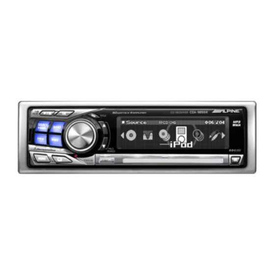
- Page 1 SERVICE MANUAL RDS MP3/WMA CD Receiver TO ALPINE Home Page 3 / 05-A 68E38380S01 CDA-9855R...
- Page 2 <Cautions for Safe Repair Work> The following cautions will prevent accidents in the workplace and will ensure safe products. *The symbols indicate caution is needed to prevent injuries and damage to property. The symbols and their meanings follow. If you ignore this symbol and handle the product incorrectly or unsafely, Warning serious injury or death may result.
-
Page 3: Table Of Contents
CDA-9855R Contents Packing Assembly Parts List Packing Method View Specifications 5 , 6 Extension Cable Adjustment Procedures 8 to 11 Block Diagram Parts Layout on P.W.Boards and Wiring Diagram 13 to 17 Schematic Diagram 18 to 26 Terminal Voltage of IC/TR... -
Page 4: Packing Assembly Parts List
CDA-9855R Packing Assembly Parts List Symbol Description Symbol Description Part No. Part No. 15D00529K02 CASE,INNER 103-4 03A60836Y01 SCR,CUS 5X7 ZN A 15D01798K03 CARRYING,CASE 103-5 60T55630W01 BAT,MGN R03(NB)UM-4 103-1 03S60820Y16 SCR,MCH 5X8 ZN A 09-02252Z01 ASSY,ANIC-0007-01A 103-2 03S60824Y01 SCR,WEV 1.7X4 ZN A... -
Page 5: Specifications
CDA-9855R Specifications < FM RADIO > Intermediate Frequency ........................10.7±0.1MHz Frequency Range ........................... 87.5 to 108.0MHz Usable Sensitivity (30dB S/N, Mono, at 98.1MHz) ..................20.2dBf -3dB Limiting Sensitivity (at 98.1MHz) ......................20.2dBf Residual Noise (Ref. 400Hz (narrow), at 98.1MHz) ..................30±10dB S/N Ratio (at 98.1MHz) - Page 6 CDA-9855R Frequency Response (Ref. 1kHz, 0dB) ............... CD : TCD-782 : 17Hz : 0±3dB 127Hz : 0±2dB 10.007kHz : 0±2dB 19.997kHz : -2±4dB MP3 : SCD-5100 (FOLDER4-128kbps) : 17Hz : 0±3dB 127Hz : 0±2dB 10.007kHz : 0±2dB 19.997kHz : -2±4dB WMA : SCD-5100 (FOLDER10-128kbps) : 17Hz : 0±3dB...
-
Page 7: Extension Cable
CDA-9855R Extension Cable *Always connect the Extension Cable when making checks of voltage and repair. DVD Deck Mechanism MAIN P.W.Board DP23S8DA CB501 CB104 CH4001 FRONT P.W.Board (1) 01E29616S01 (2) 01V37775S01 TO CONTENTS - 7 -... - Page 8 CDA-9855R - 8 - TO CONTENTS...
- Page 9 CDA-9855R (3) Control Settings Power Switch ..........ON Band Switch ......FM/MW/LW Fader Control ......Center Position T-CORR ........Non Effect Balance Control ....... Center Position ............FLAT Treble Control ......Center Position DEMO ........... OFF Bass Contro ......Center Position Others ...........
- Page 10 CDA-9855R Test Point / Step Description Connection Signal Generator Dial Control P.W.Board Adjustment Coordinates TP002 Auto Adjustment : 216kHz, (3-F) After setting up of Signal Genarator, 34dBµ 216kHz TP501 short GND and TP501 (Pull-Down) (Mod. OFF) (3-F) for 2~3 seconds.
- Page 11 CDA-9855R Test Point / Step Description Connection Signal Generator Dial Control P.W.Board Adjustment Coordinates Set up of Adjustment Mode BAND + Push at the same time. 98.1MHz, Rotary encoder is turned and noise level Noise Level Audio Output is adjustment.
-
Page 12: Block Diagram
CDA-9855R Block Diagram Pre IN/OUT Selector Slide SW Tuner unit Ai-Net E-VOL 4V AMP-8.5V Tre/Bass Selector Vol.1 Vol.2 Pre-OUT Buffe Buffer MUTE Sub Woofer Pre-OUT Buffe Buffer MUTE Front DSP+5V Pre-OUT Buffe Buffer MUTE Rear RDS Decoder MUTE OEM SUB... -
Page 13: Parts Layout On P.w.boards/Wiring Diagram
Parts Layout on P.W.Boards and Wiring Diagram(1/5) CDA-9855R TO CONTENTS BOX P.W.Board MAIN P.W.Board (Component Side View) ET601 (Component Side View) ASSY,AMP LINK55A DIN801 Q910 IC803 CB803 IC307 F801 C816 D395 C815 C911 D809 JK301 D393 D802 C801 E390 E389... - Page 14 Parts Layout on P.W.Boards and Wiring Diagram(2/5) CDA-9855R TO CONTENTS MAIN P.W.Board (Foil Side View) R595 C839 R591 C822 C818 R553 C842 C841 D394 R533 C838 C821 R857 R805 C824 D390 C840 Q806 R599 R829 Q808 Q514 C102 C388 R574...
- Page 15 Parts Layout on P.W.Boards and Wiring Diagram(3/5) CDA-9855R TO CONTENTS FRONT P.W.Board (Component Side View) SW4006 IC4002 SW4009 SW4007 R4150 R4060 R4001 R4050 RA4008 LD4028 LD4027 R4256 SW4008 RA4025 LD4022 R4092 R4206 LD4018 LD4017 LD4013 R4220 C4012 LD4006 R4051 R4052...
- Page 16 Parts Layout on P.W.Boards and Wiring Diagram(4/5) CDA-9855R TO CONTENTS OELD P.W.Board (Component Side View) C4504 C4509 R4502 R4503 R4504 R4505 R4533 R4506 R4535 ZC4501 R4536 ASSY, UEL101 (Bottom Side View) C4515 Orange Color Pattern:Component Side Pattern Blue Color Pattern:Foil Side Pattern...
- Page 17 Parts Layout on P.W.Boards and Wiring Diagram(5/5) CDA-9855R TO CONTENTS DP-S MAIN P.W.Board (Foil Side View) The patterns should be short-circuited, when the PICKUP is removed TP59 TP58 E102 from DP-S Mechanism. R102 C104 R104 C144 Q101 TP175 TP62 R103...
- Page 18 TP501 R589 470k R542 Q509 SW601 DTC114EKA SSAC120100 R541 JK501 R590 JAC,CK-3.5-14 Q508 2SB709A IC507 TC74HCT7007AFTP2-SE6 R500 R546 R591 R596 R548 100-1/4 3.3k SW602 SW,DETCT SPVG2106-E6 R603 R558 R547 R604 R559 R511 R560 SW603 SW,DETCT SPVG1107-E6 R512 R561 R569 R562 R540 D505 D504...
- Page 19 IC201 NJU7223DL1-33 C208 C210 8200p 8200p C226 R215 Z205 C243 0.45u 100p Z202 Z203 BK2125HM102 BK2125HM102 E217 47/6.3 C225 C209 C211 C228 C218 R211 C229 C230 XL201 IC204 11.28MHz C231 TDA7412 C232 C233 C234 C235 0.015 C222 C201 E202 R212 C223 0.01 3.3/50...
- Page 20 Q805 N.U. D805 D801 C815 S1G-6904 SaG-6904 C816 IC803 HA13165 E804 470/10 0.22 Q823 FMC3A D804 E805 220/6.3 S1G-6904 Q806 C804 N.U. C817 0.47 0.22 C818 C820 C821 0.22 C805 C822 N.U. N.U. C823 Q801 DTC143EKA R805 30k-1/4 D387 E387 R387 R389 R391...
- Page 21 CB101 SFW22R-1STE1 CB102 N.U. C105 N.U. R116 N.U. VT120 N.U. R111 Z101 E105 N.U. N.U. D105 S1G-6904 C103 N.U. TP104 TP105 TP106 R108 IC101 IC102 NJU7223DL1-33 D104 N.U. S1G-6904 Q102 N.U. L101 Q101 N.U. FMC3A ANT001 SA001 ASSY, ANT CABLE9851A DSP-201M-C04F VT001 C020...
- Page 22 R4243 R4242 180-1/4 82-1/4 LD4051 Q4028 Q4029 R/G/B 1304B FMC3A FMC3A R4152 240-1/4 R4129 R4153 240-1/4 R4130 R4154 240-1/4 R4177 R4131 R4178 R4021 R4132 220k R4170 C4029 C4033 Q4017 2SB1260 Q4018 2SD1328 Q4019 R4113 R4114 2SC4081 3.3k R4112 R4110 N.U. R4225 Q4020 UN5212...
- Page 23 R4087 Q4001 2SA1036K SW4014 SKRPACE010 CH4001 BTB,55323-1511 R4004 12k-1/4 R4007 1k-1/8 Q4002 UN221L Q4003 R4008 1k-1/8 UN2213 Q4004 R4010 270-1/8 UN2213 R4011 1k-1/8 R4009 1k-1/8 R4013 1k-1/8 L4001 BLM21PG221SH1D R4012 1k-1/8 C4040 100p C4011 C4001 C4041 R4090 C4042 R4209 Z4001 C4044 NFE31PT222Z1E9L SW4029...
- Page 24 L901 SD901 MA740 L902 Q912 UN211H IC901 MAX829EUK L903 Q911 ZD901 UN2211 RD3.6MB2 ET601-2 CB901 ASSY,AMP LINK 55A ET601-4 53253-0910 ET601-3 L910 220u IC910 R910 NJM2360AM SD910 SS14 G11 R909 N.U. Q910 2SD1802 L911 220u TG910 C912 N.U. R915 R916 R917 R919 2.2k-1/4...
- Page 25 CB4504 IMSA9632S-30Y R4509 R4512 R4510 100p R4508 R4514 R4532 R4515 R4534 ZC4501 ASSY,UEL101 R4531 R4511 R4536 R4535 R4506 R4505 R4504 R4503 R4502 R4501 R4516 R4533 R4529 TO P. W. BOARD TO PARTS LIST TO CONTENTS - 25 -...
- Page 26 C101 HD101 L201 E201 PICKUP, EP21A67T 0.01 47/5.5 4.7u CB101 IMSA-9616S-15Y900 L102 BK1608HM102-T R206 TP60 C202 L202 XL201 16.93MHz 4.7u TP61 Q103 C203 R202 N.U. R814 C113 R101 R108 C220 TP178 TP160 R103 N.U. RA113 R109 R110 TP177 TP161 E105 4.7k R112 C109...
- Page 27 CDA-9855R Terminal Voltage of IC/TR IC001 Voltage Note 3.16 3.11 4.96 4.96 IC002 Voltage Note Voltage Note Voltage Note 5.04 2.53 2.53 2.55 2.53 2.17 2.53 2.53 2.53 5.05 5.05 IC101 IC201 Voltage Note Voltage Note 3.31 6.57 7.49 IC202...
- Page 28 CDA-9855R IC204 Voltage Note Voltage Note Voltage Note 4.24 4.24 4.24 3.55 4.24 4.24 4.24 4.24 4.24 4.24 4.24 4.24 4.24 4.24 4.24 4.24 4.24 4.24 4.24 4.24 4.24 4.24 4.24 4.24 4.24 4.24 4.24 4.24 IC301 Voltage Note Voltage...
- Page 29 CDA-9855R IC307 Voltage Note Voltage Note Voltage Note 7.62 1.72 14.3 7.62 7.62 4.85 7.62 1.63 7.62 14.3 1.47 7.62 1.33 3.59 7.62 7.62 IC501 Voltage Note Voltage Note Voltage Note 3.33 3.33 4.95 3.33 3.33 0/3.33 3.33/0 TUNER/CD NOSE CLOSE/OPEN 3.33...
- Page 30 CDA-9855R IC502 IC503 Voltage Note Voltage Note 4.96 3.34 4.95 4.95 IC504 IC505 Voltage Note Voltage Note 8.68 4.95 4.95 IC507 Voltage Note Voltage Note Voltage Note 3.33/0 POW IC ON /OFF 4.9/0 3.33 IC508 Voltage Note Voltage Note 0/3.33 RESET ON/OFF 1.27/3.33...
- Page 31 CDA-9855R IC604 IC605 Voltage Note Voltage Note 4.95 4.95 4.95 IC802 Voltage Note Voltage Note Voltage Note 12.43 0/5.97 ANGLE action 12.43 0/4.4 ANGLE action 0/4.4 ANGLE action 0/4.7 ANGLE action 0/4.7 ANGLE action 0/4.4 ANGLE action IC803 Voltage Note...
- Page 32 CDA-9855R IC4001 Voltage Note Voltage Note Voltage Note 5.02 3.04/0.09/ BLUE/GRN/ 2.63/3.18 AMB/RED 0.08/2.79/ BLUE/GRN/ 3.55/3.47/ BLUE/GRN/ 2.72/2.92 AMB/RED 0.27/3.72 AMB/RED IC4002 Voltage Note 4.86 3.75 IC4005 Voltage Note Voltage Note Voltage Note 3.31 3.29 3.01 3.28 3.31 IC4008-1 Voltage...
- Page 33 CDA-9855R IC4008-2 Voltage Note Voltage Note Voltage Note 3.31 1.82 IC4010 IC4012 Voltage Note Voltage Note 5.02 4.74 0.02 1.26 3.33 1.82 5.02 5.01 IC4011 Voltage Note Voltage Note Voltage Note 3.36 3.36 3.36/0/0 DIM1/2/3 3.36/0 RED LED ON 0/3.36/0 DIM1/2/3 3.36...
- Page 34 CDA-9855R Note Ref. Q002 3.28 ADJCH MUTE Q003 7.78 8.48 8.55 Q004 8.49 8.55 Q005 3.29/0 0/8.54 FM/AM Q201 3.28 IF MUTE Q387 0/3.28 4.38/0 MUTE ON/OFF Q389 4.35/0 0/4.16 MUTE ON/OFF Q502 9.35 14.27 8.75 NOSE +5V Q503 9.35 14.27...
- Page 35 CDA-9855R Note Ref. Q101 3.29 3.27 CD STBY Q388 0/14.4 14.4/0 14.4/14.4 4.38/0 MUTE ON/OFF Q501 14.4 14.4 3.29 NOSE POWER Q504 3.31 3.31 3.31 VDD PULLUP Q516 0/4.87 4.84/1.95 4.93/4.87 3.27/0 RESET ON/OFF Q802 5.03/0 0/4.88 5.04/0 0.3/1.75 High Volt DET Q803 4.69...
- Page 36 CDA-9855R (CD Deck Mechanism) IC101 CD-DA PLAY MP3 PLAY CD-DA PLAY MP3 PLAY 3.32V 3.28V 3.30V 3.03V 1.64V 1.66V 1.62V 1.66V 1.66V 1.68V 1.62V 1.66V 1.70V 1.68V 2.62V 2.26V 0.26V 0.24V 1.68V 1.66V 2.54V 2.52V 1.36V 1.34V 2.04V 2.02V 0.30V 0.64V...
- Page 37 CDA-9855R IC103 CD-DA PLAY MP3 PLAY CD-DA PLAY MP3 PLAY 0.11V 0.10V 3.56V 3.50V 1.68V 1.66V 3.24V 3.24V 1.64V 1.66V 3.36V 3.35V 1.68V 1.66V 3.44V 3.44V 1.68V 1.66V 0.11V 0.10V 1.68V 1.66V 1.68V 1.64V 1.52V 1.52V 3.32V 3.30V 7.00V 7.00V 1.68V...
- Page 38 CDA-9855R IC201 CD-DA PLAY MP3 PLAY CD-DA PLAY MP3 PLAY 3.30V 3.28V 0.13V 0.10V 3.30V 3.28V 0.10V 0.10V 0.10V 0.10V 3.30V 3.28V 0.10V 0.10V 0.10V 0.10V 3.30V 0.42V-3.28V H/L 0.12V 0.10V 3.30V 0.40V-3.30V H/L 0.12V 0.10V 3.30V 3.28V 0.10V 0.10V-3.30V H/L 3.30V...
- Page 39 CDA-9855R IC303 CD-DA PLAY MP3 PLAY 0.00V 0.00V 0.00V 0.00V PULSE : 3.17V (when disc scratch is detected) 3.17V 3.17V 0.00V 0.00V 0.00V 0.00V PULSE : 3.17V (when disc scratch is detected) 0.00V 0.00V 3.17V 3.17V 3.17V 3.17V IC304 CD-DA PLAY MP3 PLAY 1.65V...
- Page 40 CDA-9855R Q101 Q102 CD-DA PLAY MP3 PLAY CD-DA PLAY MP3 PLAY 2.54V 2.56V 3.20V 3.22V 2.24V 2.26V 1.66V 1.66V 3.20V 3.18V 3.24V 3.22V Q301 CD-DA PLAY MP3 PLAY 0.00V 0.00V PULSE : 3.17V (when disc scratch is detected) 0.00V 0.00V 3.17V...
- Page 41 CDA-9855R Description of IC Terminal D70F3263YGC : IC501 Symbol Terminal Description AVref1 AVref power supply input terminal. (connect to VDD) AVss GND connect terminal for A/D Converter. DSP CLK DSP CLOCK output terminal. DSP DATA I/O DSP DATA output terminal.
- Page 42 CDA-9855R Symbol Terminal Description F-START Front u-COM communication start output terminal. F-RESET Front u-COM RESET signal output terminal. AMP DATA IN AMP LINK DATA input terminal. AMP DATA OUT AMP LINK DATA output terminal. AMP CLK AMP LINK CLOCK output terminal.
- Page 43 CDA-9855R Symbol Terminal Description Multi-Path signal input terminal. AFC signal input terminal. SSTOP SEEK STOP input terminal. TUNER S/M level input terminal. NOSE DET NOSE installation detect terminal. D70F3261YGC : IC4011 Symbol Terminal Description AVREF0 Reference voltage input terminal for A/D Converter.
- Page 44 CDA-9855R Symbol Terminal Description RGB CS RGB Chip Select output terminal. RGB RST RGB Reset output terminal. RGB DATA RGB Serial Data output terminal. RGB CLK RGB Serial Clock output terminal. External ROM address port terminal. WAIT WAIT terminal. CLK OUT CLK output terminal to OELD Controller No connect terminal.
- Page 45 CDA-9855R Symbol Terminal Description External ROM data port terminal. ROM-SEL2(NC) No connect terminal. ROM-SEL1 64Mbit ROM SEL control terminal. SEG-SEL External ROM address bus terminal. DRIV-RESET OELD Driver Reset terminal. CO-RST OELD Controller Reset terminal. VHH-CONT2 OELD Vhh power supply control terminal.
- Page 46 CDA-9855R Symbol Terminal Description /BUCK CLOCK output terminal for SERVO_LSI (TC94A14FA) interface. /CCE Chip enable output terminal for SERVO_LSI (TC94A14FA) interface. /CD_RESET SERVO_LSI (TC94A14FA) RESET output terminal. ZMUTEIN 0 detection flag input terminal for SERVO_LSI (TC94A14FA) interface. NC(PULL-DOWN) Pull-down connect terminal.
-
Page 47: Exploded View (Cabinet)
Exploded View (Cabinet)(1/2) CDA-9855R ZC4501 ANT001 M802 JK301 ET601 CB803 JK501 DIN801 SW602 CH4001 SW603 SW4027 CH501 TO PARTS LIST TO CONTENTS - 47 -... - Page 48 CDA-9855R Exploded View (Cabinet)(2/2) (Back Side) (Back Side) CH801 M801 ..pint of GREASE applied. GREASE,G-1017(11T65588Y01) GREASE,G-8007(11S41558Y01) TO PARTS LIST TO CONTENTS - 48 -...
-
Page 49: Exploded View (Cd Deck Mechanism) (Dp23S8Da)
CDA-9855R Exploded View (CD Deck Mechanism) (DP23S8DA) TO PARTS LIST TO CONTENTS - 49 -...
Need help?
Do you have a question about the CDA-9855R and is the answer not in the manual?
Questions and answers