Table of Contents
Advertisement
This document is printed on chlorine free (ECF) paper.
PA
011869
MG166CX-USB/MG166CX: xxxxxx-xxxxx
MG166C-USB/MG166C: xxxxxx-xxxxx
SERVICE MANUAL
MG166CX-USB
I CONTENTS
SPECIFICATIONS
.............................................................................. 7
.......................................................................... 44/52
IC & DIODE FIGURES
BLOCK & LEVEL DIAGRAM
Copyright (c) Yamaha Corporation. All rights reserved.
.................................................................. 3/5
......................................................... 8
.................................. 12
............................................................. 13
........................................ 14
..................................................... 19
.......................................................... 23
.................................................. 27
...................................................... 30
........................................................... 33
HAMAMATSU, JAPAN
MG166C-USB
07.08
Advertisement
Table of Contents

Related Manuals for Yamaha MG 166CX-USB


Summary of Contents for Yamaha MG 166CX-USB
- Page 1 ............33 INSPECTIONS ................44/52 PARTS LIST IC & DIODE FIGURES BLOCK & LEVEL DIAGRAM This document is printed on chlorine free (ECF) paper. CIRCUIT DIAGRAM 011869 MG166CX-USB/MG166CX: xxxxxx-xxxxx HAMAMATSU, JAPAN MG166C-USB/MG166C: xxxxxx-xxxxx Copyright (c) Yamaha Corporation. All rights reserved. 07.08...
-
Page 2: Important Notice
IMPORTANT NOTICE This manual has been provided for the use of authorized Yamaha Retailers and their service personnel. It has been assumed that basic service procedures inherent to the industry, and more specifically Yamaha Products, are already known and understood by the users, and have therefore not been restated. -
Page 3: Specifications
MG166CX-USB/MG166CX/MG166C-USB/MG166C SPECIFICATIONS • Electrical Specifications • General Specifications... - Page 4 MG166CX-USB/MG166CX/MG166C-USB/MG166C • Analog Input Specifications • Analog Output Specifications • Digital Input/Output Specifications (MG166CX-USB, MG166C-USB only)
- Page 5 MG166CX-USB/MG166CX/MG166C-USB/MG166C...
- Page 6 MG166CX-USB/MG166CX/MG166C-USB/MG166C...
- Page 7 MG166CX-USB/MG166CX/MG166C-USB/MG166C DIMENSIONS Unit: mm MG166CX-USB...
-
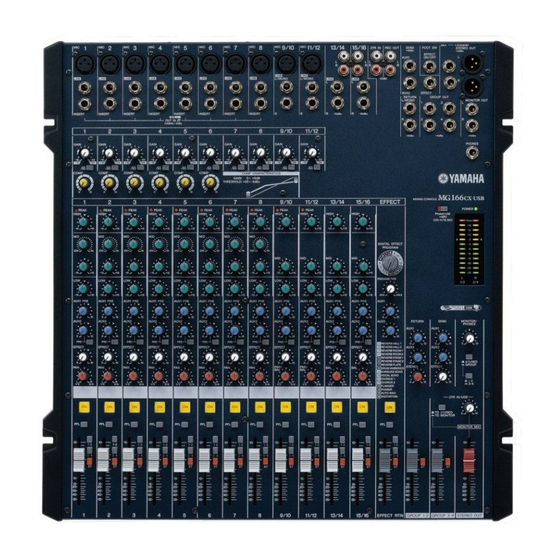
Page 8: Panel Layout
MG166CX-USB/MG166CX/MG166C-USB/MG166C PANEL LAYOUT • Channel Control Section AUX1, AUX2, EFFECT (MG166CX-USB, MG166CX) AUX1, AUX2, AUX3 (MG166C-USB, MG166C) MIC Input Jacks Channels Channels Channels Channels 1 to 6 7 and 8 9/10 and 11/12 13/14 and 15/16 LINE Input Jacks (monaural channels) (Monaural) (Monaural) (Stereo) - Page 9 MG166CX-USB/MG166CX/MG166C-USB/MG166C * Only the MG166CX-USB and MG166CX have digital effects. • Digital Effects Section FOOT SWITCH Jack PROGRAM Dial PARAMETER Control AUX Control ON Switch PFL Switch 1-2 Switch 3-4 Switch ST Switch EFFECT RTN Fader...
- Page 10 MG166CX-USB/MG166CX/MG166C-USB/MG166C • Master Control Section * 2, D AUX1, AUX2, EFFECT (MG166CX-USB, MG166CX) AUX1, AUX2, AUX3 (MG166C-USB, MG166C) USB Connector (MG166CX-USB/MG166C-USB only) Rear panel SEND Jacks (AUX, EFFECT) GROUP OUT (1 to 4) Jacks REC OUT (L, R) Jacks 2TR IN Jacks RETURN L (MONO), R Jacks STEREO OUT (L, R) Jacks •...
- Page 11 MG166CX-USB/MG166CX/MG166C-USB/MG166C • Connector Polarities Input and Output Jacks Polarities Configurations INPUT OUTPUT Pin 1: Ground MIC INPUT, STEREO OUT Pin 2: Hot (+) Pin 3: Cold (–) XLR Jack LINE INPUT (monaural channels) GROUP OUT, STEREO OUT, Tip: Hot (+) MONITOR OUT, AUX SEND, Ring: Cold (–) Ring...
-
Page 12: Circuit Board Layout
MG166CX-USB/MG166CX/MG166C-USB/MG166C CIRCUIT BOARD LAYOUT Rear (MG166CX-USB) (MG166C-USB) PS16X JACK16X PS16 JACK16 (MG166CX-USB, MG166CX) MIX16X MIX16 Front... -
Page 13: Wiring Diagram
MG166CX-USB/MG166CX/MG166C-USB/MG166C WIRING DIAGRAM (MG166CX-USB, MG166C-USB only) PS16X PS16X CN101 CN102 CN104 CN101 (9P) (3P) (5P) (7P) JACK16X JACK16 CN903 (9P) CN001 W401 W701 W801 W002 W001 W003 W004 (3P) (9P) (9P) (9P) (9P) (9P) (9P) (6P) W101 W201 W301 (9P) (9P) (9P) CN401... - Page 14 MG166CX-USB/MG166CX/MG166C-USB/MG166C OVERALL ASSEMBLY WIRING The inside room of this product is very little because a lot of units are installed fully. To prevent the panel’s coming up and other things when assembling, perform the cable connection according to the followings. 1.
- Page 15 MG166CX-USB/MG166CX/MG166C-USB/MG166C MG166CX-USB, MG166CX The wiring of the MIX16X circuit board and JACK16X circuit board. MG166C-USB, MG166C The wiring of the MIX16 circuit board and JACK16 circuit board. 2-1. MG166CX-USB, MG166CX Install the JACK16X circuit board [Ref. 250]. Note: Pass the connector assembly PS7P [Ref. 40], connector assembly PS3P [Ref. 50] and connector assembly PS5P [* 1 Ref.
- Page 16 MG166CX-USB/MG166CX/MG166C-USB/MG166C Whole picture JACK16(X) K103 JACK16(X) CN903 MIX16(X) K051 JACK16(X) K101 JACK16(X) CN001 JACK16(X) K102 MIX16(X) MIX16(X) MIX16(X) MIX16(X) MIX16(X) CN053 MIX16(X) CN401 CN701 CN801 CN001 CN004 MIX16(X) MIX16(X) MIX16(X) MIX16(X) CN101 CN201 CN301 MIX16(X) CN003 CN002 MIX16(X) CN051 2-2. The wiring of the connector assemblies from the Inner Chassis assembly. MG166CX-USB, MG166CX Ref.
- Page 17 MG166CX-USB/MG166CX/MG166C-USB/MG166C Note: In the MG166CX, bend the K101 and K102 of JACK16X circuit board in the direction where the jumper leads are not installed. (See the picture below) MG166C-USB, MG166C Ref. Note Part Wiring Point Connector Assembly JACK16 circuit board Fix the connector assembly with the style pins [Ref.
- Page 18 MG166CX-USB/MG166CX/MG166C-USB/MG166C Junper-Wire Connector assembly PS7P Connector assembly PS7P Connector assembly PS5P Connector assembly PS5P Connector assembly PS5P Connector assembly PS5P 2-3. MG166CX-USB, MG166CX Connect the ten (10) jumper wires of JACK16X circuit board to the MIX16X circuit board. (MG166CX-USB, MG166CX) Note: Bend the jumper wires according to the picture above.
- Page 19 MG166CX-USB/MG166CX/MG166C-USB/MG166C MG166CX-USB/MG166CX I MG166CX-USB/MG166CX DISASSEMBLY PROCEDURES Top Cover (Time required: 12 min.) Remove the twelve (12) fader knobs marked [490], three (3) fader knobs marked [500] and fader knob marked [510] and knob select marked [300]. (Fig. 1) Remove the fifteen (15) screws marked [400], sixteen (16) screws marked [410], four (4) screws marked [420], six (6) screws marked [430], thirty-nine (39) hexagonal nuts and thirty-nine (39) washers.
- Page 20 MG166CX-USB/MG166CX/MG166C-USB/MG166C MG166CX-USB/MG166CX MIX16X Circuit Board, DSP Circuit Board and JACK16X Circuit Board (Time required: 18 min.) Remove the top cover. (See procedure 1.) Disconnect the fourteen (14) connectors. Remove the fourteen (14) screws marked [350] and a hexagonal spacer marked [360]. (Fig. 2) Release the eight (8) hooks and remove the MIX16X circuit board with DSP circuit board.
- Page 21 MG166CX-USB/MG166CX/MG166C-USB/MG166C MG166CX-USB/MG166CX PS16X Circuit Board (Time required: 18 min.) Remove the top cover. (See procedure 1.) Remove the MIX16X circuit board, DSP circuit board and JACK16X circuit board. (See procedure 2.) Remove the three (3) screws marked [190], three (3) screws marked [200] and three (3) screws marked [220].
- Page 22 MG166CX-USB/MG166CX/MG166C-USB/MG166C MG166CX-USB/MG166CX USB Circuit Board (MG166CX-USB only) (Time required: 18 min.) Remove the top cover. (See procedure 1.) Remove the MIX16X circuit board, DSP circuit board and JACK16X circuit board. (See procedure 2.) Remove the two (2) screws marked [110] and remove the USB assembly.
- Page 23 MG166CX-USB/MG166CX/MG166C-USB/MG166C MG166C-USB/MG166C I MG166C-USB/MG166C DISASSEMBLY PROCEDURES Top Cover (Time required: 12 min.) Remove the twelve (12) fader knobs marked [490], two (2) fader knobs marked [500] and fader knob marked [510]. (Fig. 1) Remove the fifteen (15) screws marked [400], sixteen (16) screws marked [410], three (3) screws marked [420], six (6) screws marked [430], thirty-eight (38) hexagonal nuts and thirty-eight (38) washers.
- Page 24 MG166CX-USB/MG166CX/MG166C-USB/MG166C MG166C-USB/MG166C MIX16 Circuit Board and JACK16 Circuit Board (Time required: 18 min.) Remove the top cover. (See procedure 1.) Remove the fourteen (14) screws marked [350]. (Fig. 2) Release the eight (8) hooks and remove the MIX16 cir- cuit board. (Fig. 2) Remove the three (3) screws marked [300] and remove the JACK16 circuit board.
- Page 25 MG166CX-USB/MG166CX/MG166C-USB/MG166C MG166C-USB/MG166C PS16 Circuit Board (Time required: 18 min.) Remove the top cover. (See procedure 1.) Remove the MIX16 circuit board and JACK16 circuit board. (See procedure 2.) Remove the three (3) screws marked [190], three (3) screws marked [200] and three (3) screws marked [220]. The inner chassis with heatsink assembly and USB as- sembly (MG166C-USB only) can be removed.
- Page 26 MG166CX-USB/MG166CX/MG166C-USB/MG166C MG166C-USB/MG166C USB Circuit Board (MG166C-USB only) (Time required: 18 min.) Remove the top cover. (See procedure 1.) Remove the MIX16 circuit board and JACK16 circuit board. (See procedure 2.) Remove the two (2) screws marked [110] and remove the USB assembly. (Fig. 5) Unsolder the shield USB mounting solder (2 locations) and separate the shield USB from the USB circuit board.
-
Page 27: Lsi Pin Description
MG166CX-USB/MG166CX/MG166C-USB/MG166C LSI PIN DESCRIPTION CONTENTS • AK5381VT-E2 (X5219A00) ADC (Analog to Digital Converter) .... 27 • MX23L8103TC-90G (X5922A00) CPU ............. 28 • PCM1742KEG/2K (X3538A00) DAC (Digital to Analog Converter) ..27 • PCM2900E/2K (X7143A00) CODEC ............28 • YMW767-VTZ (X6055A00) CPU .............. 29 •... - Page 28 MG166CX-USB/MG166CX/MG166C-USB/MG166C • PCM2900E/2K (X7143A00) CODEC USB: IC101 NAME FUNCTION NAME FUNCTION USB differential input/output plus VOUTR DAC analog output for R-channel USB differential input/output minus VOUTL DAC analog output for L-channel VBUS Connect to USB power (VBUS) VCCP1I Internal analog power supply for PLL DGNDU Digital ground for USB transceiver AGNDP...
- Page 29 MG166CX-USB/MG166CX/MG166C-USB/MG166C • YMW767-VTZ (X6055A00) CPU (SWLO1B) DSP: ICM07 NAME FUNCTION NAME FUNCTION Ground Ground TESTN Input for test Power supply +3.3 V PLLBPN PLL bypass select LBN/LWRN/PF6 External memory lower-byte enable / Port F PLLV PLL power supply +2.5 V UBN/UWRN/PF7 External memory upper-byte enable / Port F ...
-
Page 30: Ic Block Diagram
MG166CX-USB/MG166CX/MG166C-USB/MG166C IC BLOCK DIAGRAM • PST596DNR (X0165A00) System Reset DSP: ICM03 Delay – – • NJM2068M-D (TE2) (X3505A00) • KIA7812API (X4153A00) Dual Operational Amplifier Regulator +12V JACK16: IC702, 752 PS16: IC105 MIX16: IC001, 003, 901, 902, 951, 952, ICM01 USB: IC103, 104 INPUT Q11-1... - Page 31 MG166CX-USB/MG166CX/MG166C-USB/MG166C • KIA7805API/P (X4928A00) • KIA7815API (X4930A00) Regulator +5V Regulator +15V PS16: IC106, 107 PS16: IC101, 103 INPUT INPUT Q11-1 Q11-1 OUTPUT OUTPUT COMMON (GND) COMMON (GND) • KIA7915PI (X4931A00) Regulator -15V PS16: IC102, 104 R 22 R 21 Q 28 Q 17 Q 21 R 13...
- Page 32 MG166CX-USB/MG166CX/MG166C-USB/MG166C • NJM4580M-D (TE2) (X5025A00) • BA10339F (X6266A00) Dual Operational Amplifier Comparator JACK16: IC071, 072, 701, 751 MIX16: ICM06-11 OUT3 OUT2 OUT4 OUT1 2, 6 1, 7 OUTPUT –INPUT +INPUT –IN1 +IN4 3, 5 – – –IN4 +IN1 +IN3 –IN2 –...
-
Page 33: Circuit Boards
MG166CX-USB/MG166CX/MG166C-USB/MG166C MG166CX-USB/MG166CX CIRCUIT BOARDS CONTENTS • DSP Circuit Board (X7687D0) ........... 33 • JACK16X/JACK16 Circuit Board (X8282C0) ........... 36 • MIX16X/MIX16 Circuit Board (X8281C0) ........... 40 • PS16X/PS16 Circuit Board (X8285C0) ........... 34 • USB Circuit Board (X7196C0) ........... 35 Note: See parts list for details of circuit board component parts. - Page 34 MG166CX-USB/MG166CX/MG166C-USB/MG166C MG166CX-USB/MG166CX MG166C-USB/MG166C • PS16X/PS16 Circuit Board to JACK16 CN001 to MIX16 CN051 to MIX16 CN053 Component side 2NA-WJ98970...
- Page 35 MG166CX-USB/MG166CX/MG166C-USB/MG166C MG166CX-USB MG166C-USB • USB Circuit Board to JACK16 CN903 Component side Pattern side 2NA-WG33610...
- Page 36 MG166CX-USB/MG166CX/MG166C-USB/MG166C MG166CX-USB/MG166CX MG166C-USB/MG166C • JACK16X/JACK16 Circuit Board Reduction: 4/5 to MIX16 CN101 to MIX16 CN201 to MIX16 CN301 to MIX16 CN401 Component side 2NA-WJ26360...
- Page 37 MG166CX-USB/MG166CX/MG166C-USB/MG166C MG166CX-USB/MG166CX MG166C-USB/MG166C Reduction: 4/5 to USB CN101 to MIX16 CN801 to MIX16 CN001 to MIX16 CN003 to MIX16 CN004 to PS16 CN102 to MIX16 CN002 CN401 to MIX16 CN701 Component side 2NA-WJ26360...
- Page 38 MG166CX-USB/MG166CX/MG166C-USB/MG166C MG166CX-USB/MG166CX MG166C-USB/MG166C • JACK16X/JACK16 Circuit Board Reduction: 4/5 Pattern side 2NA-WJ26360...
- Page 39 MG166CX-USB/MG166CX/MG166C-USB/MG166C MG166CX-USB/MG166CX MG166C-USB/MG166C Reduction: 4/5 Pattern side 2NA-WJ26360...
- Page 40 MG166CX-USB/MG166CX/MG166C-USB/MG166C MG166CX-USB/MG166CX MG166C-USB/MG166C • MIX16X/MIX16 Circuit Board to J to JACK16 W401 to JACK16 W101 to JACK16 W201 to JACK16 W301 Reduction: 3/5 Component side 2NA-WJ26330...
- Page 41 MG166CX-USB/MG166CX/MG166C-USB/MG166C MG166CX-USB/MG166CX MG166C-USB/MG166C to JACK16 W701 to JACK16 W002 to JACK16 W004 to DSP CNM02 to PS16 CN104 to JACK16 W801 to JACK16 W001 to JACK16 W003 to PS16 CN101 Reduction: 3/5 Component side 2NA-WJ26330...
- Page 42 MG166CX-USB/MG166CX/MG166C-USB/MG166C MG166CX-USB/MG166CX MG166C-USB/MG166C • MIX16X/MIX16 Circuit Board Reduction: 3/5 Pattern side 2NA-WJ26330...
- Page 43 MG166CX-USB/MG166CX/MG166C-USB/MG166C MG166CX-USB/MG166CX MG166C-USB/MG166C Reduction: 3/5 Pattern side 2NA-WJ26330...
- Page 44 MG166CX-USB/MG166CX/MG166C-USB/MG166C INSPECTIONS Measurement Conditions Environment • Temperature: From 5 °C to 40 °C. • Humidity: From 30 % to 90 %. Power Source The voltage is within ±10 %. AC adaptor PA-30 should be used. • U : 120 V (WE524200) •...
- Page 45 MG166CX-USB/MG166CX/MG166C-USB/MG166C PFL switch ON when taking measurement only / OFF otherwise 1-2, 3-4 switch ON when taking measurement only / OFF otherwise ST switch ON when taking measurement only / OFF otherwise Channel fader Maximum • ST INPUT (13/14, 15/16) EQ (HIGH, LOW) GAIN control CENTER AUX1, AUX2, AUX3 level control...
- Page 46 MG166CX-USB/MG166CX/MG166C-USB/MG166C Table 2-6-1 CH INPUT 1-8 AUX3 SEND GROUP MONITOR MONITOR INPUT ST OUT AUX1 AUX2 SEND (MG166C-USB, MG166C) MONITOR INPUT GAIN OUT (L, R) OUT (L, R) LEVEL SEND EFFECT SEND OUT (L, R) 1-2/3-4 (MG166CX-USB, MG166CX) PRE OFF PRE ON +1.5 ±...
- Page 47 MG166CX-USB/MG166CX/MG166C-USB/MG166C Frequency Characteristic In the signal route 1 to 8 specified in the table 2-6-1 to 2-6-6, check the 20 Hz and 20 kHz frequency response of each output is within the range of +1/-2.5 dB compared with the 1 kHz (0 dB). When the GAIN control is set to maximum, only 20 Hz frequency response is within the range of +1/-4.5 dB compared with the 1 kHz (0 dB).
- Page 48 MG166CX-USB/MG166CX/MG166C-USB/MG166C 2-12 Lighting Check of LEVEL meters Check the “0” indicator of meter lights up when the output level at ST OUT (L, R) is +4 ± 2 dBu. Move the ST master fader and check the indicators light up in order from “-30” to “PEAK”. 2-13 Distortion In the signal routes 3 to A specified in the table 2-6-1 to 2-6-6, set the GAIN controls to the position specified in the table (except PHONES), and apply the frequency 20 Hz, 1 kHz and 20 kHz.
- Page 49 MG166CX-USB/MG166CX/MG166C-USB/MG166C 2-17 COMP 2-17-1 GAIN With controls set as specified in the section 2-2, set the COMP control of channels 1-6 to maximum. Then check the output level obtained at INSERT OUT 1-6 is within the range specified in the table 2-17-1. Table 2-17-1 CH INPUT 1-6 INPUT LEVEL...
- Page 50 MG166CX-USB/MG166CX/MG166C-USB/MG166C 2-18 DIGITAL EFFECT (MG166CX-USB, MG166CX) Set the CH1 as follows and input -60 dBu signal to CH1 MIC. Set EFFECT RTN fader and EFFECT RTN AUX VR to maximum and check the output level is the value specified in the Table 2-18.
- Page 51 MG166CX-USB/MG166CX/MG166C-USB/MG166C Others Execute each test with controls set effective. Effect (MG166CX-USB, MG166CX) Check the effect program [1], [6], [11] and [16] are effective respectively. Check the output signal can be controlled with the parameter volume in each effect program. Check the allophone can not be heard when the program is changed. PHANTOM Connect a 10 kΩ...
- Page 52 MG166CX-USB/MG166CX/MG166C-USB/MG166C...
- Page 53 MG166CX-USB/MG166CX/MG166C-USB/MG166C...
- Page 54 MG166CX-USB/MG166CX/MG166C-USB/MG166C AUX3 SEND GROUP MONITOR MONITOR ST OUT AUX1 AUX2 SEND (MG166C-USB, MG166C) MONITOR OUT (L, R) OUT (L, R) SEND EFFECT SEND OUT (L, R) 1-2/3-4 (MG166CX-USB, MG166CX) PRE OFF PRE ON +1.5 ± 2 dBu *1 +1.5 ± 2 dBu *1 +4 ±...
- Page 55 MG166CX-USB/MG166CX/MG166C-USB/MG166C +12 ± 2 dB -12 ± 2 dB +15 ± 2.5 dB -15 ± 2.5 dB +15 ± 2.5 dB -15 ± 2.5 dB +12 ± 2 dB -12 ± 2 dB +12 ± 2 dB HIGH 10 kHz -12 ±...
- Page 56 MG166CX-USB/MG166CX/MG166C-USB/MG166C STEREO OUT GROUP OUT AUX1, AUX2, AUX3 SEND (MG166C-USB, MG166C) MONITOR OUT (L, R) (L, R) (1-4) AUX1, AUX2, EFFECT SEND (MG166CX-USB, MG166CX) -78 dBu -80 dBu -75 dBu -72 dBu -98 dBu -100 dBu -100 dBu -85 dBu...
- Page 57 MG166CX-USB/MG166CX/MG166C-USB/MG166C CH INPUT 1-6 INSERT OUT 1-6 +3 ± 2 dBu -65 dBu CH INPUT 1-6 INSERT OUT 1-6 +3.5 ± 1 dBu -55 dBu 20 Hz 5.0 % 1 kHz 1.0 % 20 kHz 1.0 % 100% 100%...
- Page 58 MG166CX-USB/MG166CX/MG166C-USB/MG166C PARAMETER OUTPUT EFFECT RTN PFL ST L,R GROUP 1-4 MONITOR L MONITOR R PHONE -20 dBu (INSERT) MONITOR OUT L MONITOR OUT R +16 ± 3 dBu +16 ± 3 dBu...
- Page 59 MG166CX-USB/MG166CX/MG166C-USB/MG166C...
-
Page 60: Parts List
MG166CX-USB/MG166CX/MG166C-USB/MG166C PARTS LIST I CONTENTS MG166CX-USB/MG166CX OVERALL ASSEMBLY ..........2 MG166CX-USB/MG166CX HEATSINK ASSEMBLY ......5 MG166C-USB/MG166C OVERALL ASSEMBLY ............6 MG166C-USB/MG166C HEATSINK ASSEMBLY ........9 ELECTRICAL PARTS ............10 Notes: DESTINATION ABBREVIATIONS Australian model South African model British model Chinese model Canadian model South-east Asia model German model... - Page 61 MG166CX-USB/MG166CX/MG166C-USB/MG166C MG166CX-USB/MG166CX MG166CX-USB/MG166CX OVERALL ASSEMBLY Accessories of Phone Jack Accessories of Phone Jack Priority Screw MG166CX-USB Heatsink Assembly (See Page 5) Priority Screw Priority Screw Priority Screw...
- Page 62 MG166CX-USB/MG166CX/MG166C-USB/MG166C MG166CX-USB/MG166CX PART NO. DESCRIPTION REMARKS REF NO. RANK OVERALL ASSEMBLY MG166CX,MG166CX-USB Overall Assembly MG166CX (WJ54960) Overall Assembly MG166CX-USB (WJ54950) WJ449700 Bottom Case Assembly MG166CX WJ449800 Bottom Case Assembly MG166CX-USB Bottom Case MG166CX (WJ44930) Bottom Case MG166CX-USB (WJ44920) WH091200 Foot Shield Sheet (WJ28190) WJ653900...
- Page 63 MG166CX-USB/MG166CX/MG166C-USB/MG166C MG166CX-USB/MG166CX PART NO. DESCRIPTION REMARKS REF NO. RANK WE523900 AC Adaptor PA-30 H WE524100 AC Adaptor PA-30 K WE523600 AC Adaptor PA-30 A WE523700 AC Adaptor PA-30 B WE523800 AC Adaptor PA-30 CHN V 8 1 0 0 4 0 0 USB Cable 4P 1.5m USB(A-B) MG166CX-USB...
-
Page 64: Bottom View
MG166CX-USB/MG166CX/MG166C-USB/MG166C MG166CX-USB/MG166CX MG166CX-USB/MG166CX HEATSINK ASSEMBLY Bottom view PART NO. DESCRIPTION REMARKS REF NO. RANK Heatsink Assembly MG166CX,MG166CX-USB (WJ65430) WJ264200 Circuit Board PS16X Heatsink PS B (WJ65410) Silicone Grease X-113A G746 (VA79810) WE774300 Bind Head Tapping Screw-B MFZN2W3 WE774300 Bind Head Tapping Screw-B MFZN2W3 : New Parts RANK: Japan only... - Page 65 MG166CX-USB/MG166CX/MG166C-USB/MG166C MG166C-USB/MG166C MG166C-USB/MG166C OVERALL ASSEMBLY Accessories of Phone Jack Accessories of Phone Jack Priority Screw MG166C-USB Heatsink Assembly (See Page 9) Priority Screw Priority Screw Priority Screw...
- Page 66 MG166CX-USB/MG166CX/MG166C-USB/MG166C MG166C-USB/MG166C PART NO. DESCRIPTION REMARKS REF NO. RANK OVERALL ASSEMBLY MG166C,MG166C-USB Overall Assembly MG166C (WJ54980) Overall Assembly MG166C-USB (WJ54970) WJ449700 Bottom Case Assembly MG166C WJ449800 Bottom Case Assembly MG166C-USB Bottom Case MG166C (WJ44930) Bottom Case MG166C-USB (WJ44920) WH091200 Foot Shield Sheet (WJ28190) WJ653900...
- Page 67 MG166CX-USB/MG166CX/MG166C-USB/MG166C MG166C-USB/MG166C PART NO. DESCRIPTION REMARKS REF NO. RANK X8515A00 DVD-ROM 8E94 MG166C-USB V 8 1 0 0 4 0 0 USB Cable 4P 1.5m USB(A-B) MG166C-USB AC Adaptor (J) OUTPUT: AC35VCT 0.94A (2) GND (1) AC (3) AC : New Parts RANK: Japan only...
- Page 68 MG166CX-USB/MG166CX/MG166C-USB/MG166C MG166C-USB/MG166C MG166C-USB/MG166C HEATSINK ASSEMBLY Bottom view PART NO. DESCRIPTION REMARKS REF NO. RANK Heatsink Assembly MG166C,MG166C-USB (WJ65420) WJ264100 Circuit Board PS16 Heatsink PS B (WJ65410) Silicone Grease X-113A G746 (VA79810) WE774300 Bind Head Tapping Screw-B MFZN2W3 WE774300 Bind Head Tapping Screw-B MFZN2W3 : New Parts RANK: Japan only...
- Page 69 MG166CX-USB/MG166CX/MG166C-USB/MG166C MG166CX-USB/MG166CX ELECTRICAL PARTS PART NO. DESCRIPTION REMARKS REF NO. RANK ELECTRICAL PARTS MG166CX,MG166CX-USB MG166C,MG166C-USB WH108400 Circuit Board MG166CX,MG166CX-USB (WH10870)(X7687D0) WJ263700 Circuit Board JACK16X MG166CX,MG166CX-USB (X8282C0) WJ263600 Circuit Board JACK16 MG166C,MG166C-USB (X8282C0) WJ263400 Circuit Board MIX16CX MG166CX,MG166CX-USB (X8281C0) WJ263300 Circuit Board MIX16 MG166C,MG166C-USB (X8281C0)
- Page 70 MG166CX-USB/MG166CX/MG166C-USB/MG166C MG166CX-USB/MG166CX PART NO. DESCRIPTION REMARKS REF NO. RANK CM79 US064100 Ceramic Capacitor-B (chip) 0.01uF 50V K US064100 Ceramic Capacitor-B (chip) 0.01uF 50V K CM82 US035100 Ceramic Capacitor-B (chip) 0.1uF 16V K CM83 US035100 Ceramic Capacitor-B (chip) 0.1uF 16V K CM85 US035100 Ceramic Capacitor-B (chip)
- Page 71 MG166CX-USB/MG166CX/MG166C-USB/MG166C MG166CX-USB/MG166CX MG166C-USB/MG166C JACK16X/JACK16 PART NO. DESCRIPTION REMARKS REF NO. RANK WJ263700 Circuit Board JACK16X MG166CX,MG166CX-USB (X8282C0) WJ263600 Circuit Board JACK16 MG166C,MG166C-USB (X8282C0) Jumper Wire SMV2J P=2.0 9-50 (WH52570) Jumper Wire SMV2J P=2.0 6-50 (WH51440) Jumper Wire 0.55 TIN (VA07890) WH362000 Knob Joint VRS NATURAL...
- Page 72 MG166CX-USB/MG166CX/MG166C-USB/MG166C MG166CX-USB/MG166CX MG166C-USB/MG166C JACK16X/JACK16 PART NO. DESCRIPTION REMARKS REF NO. RANK C117 UA654820 Mylar Capacitor 0.082uF 50V J C118 US062100 Ceramic Capacitor-SL(chip) 100pF 50V J C119 UR867100 Electrolytic Cap. 10uF C120 UR857470 Electrolytic Cap. 47uF -122 UR857470 Electrolytic Cap. 47uF C123 US062100 Ceramic Capacitor-SL(chip)
- Page 73 MG166CX-USB/MG166CX/MG166C-USB/MG166C MG166CX-USB/MG166CX MG166C-USB/MG166C JACK16X/JACK16 PART NO. DESCRIPTION REMARKS REF NO. RANK C253 WH167700 Electrolytic Cap. 10uF C254 WH167700 Electrolytic Cap. 10uF C255 UR867100 Electrolytic Cap. 10uF C256 UR867100 Electrolytic Cap. 10uF C257 US062470 Ceramic Capacitor-SL(chip) 470pF 50V J -259 US062470 Ceramic Capacitor-SL(chip) 470pF 50V J C260...
- Page 74 MG166CX-USB/MG166CX/MG166C-USB/MG166C MG166CX-USB/MG166CX MG166C-USB/MG166C JACK16X/JACK16 PART NO. DESCRIPTION REMARKS REF NO. RANK C369 UR867100 Electrolytic Cap. 10uF C370 UR857470 Electrolytic Cap. 47uF -372 UR857470 Electrolytic Cap. 47uF C373 US062100 Ceramic Capacitor-SL(chip) 100pF 50V J C374 US061680 Ceramic Capacitor-SL(chip) 68pF 50V J C375 US061220 Ceramic Capacitor-CH(chip)
- Page 75 MG166CX-USB/MG166CX/MG166C-USB/MG166C MG166CX-USB/MG166CX MG166C-USB/MG166C JACK16X/JACK16 PART NO. DESCRIPTION REMARKS REF NO. RANK C724 US062100 Ceramic Capacitor-SL(chip) 100pF 50V J C725 US062100 Ceramic Capacitor-SL(chip) 100pF 50V J C726 US061470 Ceramic Capacitor-CH(chip) 47pF 50V J C727 US061470 Ceramic Capacitor-CH(chip) 47pF 50V J C728 UR867100 Electrolytic Cap.
- Page 76 MG166CX-USB/MG166CX/MG166C-USB/MG166C MG166CX-USB/MG166CX MG166C-USB/MG166C JACK16X/JACK16 PART NO. DESCRIPTION REMARKS REF NO. RANK CM05 UR838100 Electrolytic Cap. 100uF 16V UR838100 Electrolytic Cap. 100uF 16V CN001 VB389900 Connector Base Post PH 3P TE CN903 VB390500 Connector Base Post PH 9P TE D101 VR496500 Diode (chip) MA111 FLAT TP D101...
- Page 77 MG166CX-USB/MG166CX/MG166C-USB/MG166C MG166CX-USB/MG166CX MG166C-USB/MG166C JACK16X/JACK16 PART NO. DESCRIPTION REMARKS REF NO. RANK JK021 WH919000 Phone Jack ST MSJ-064-30B B RETURN L(MONO) JK022 WH919000 Phone Jack ST MSJ-064-30B B RETURN R JK041 WH919000 Phone Jack ST MSJ-064-30B B AUX1 SEND JK042 WH919000 Phone Jack ST MSJ-064-30B B AUX2 SEND...
- Page 78 MG166CX-USB/MG166CX/MG166C-USB/MG166C MG166CX-USB/MG166CX MG166C-USB/MG166C JACK16X/JACK16 PART NO. DESCRIPTION REMARKS REF NO. RANK Q302 V 7 4 2 1 7 0 0 Transistor (chip) 2SC3324 GR,BL Q303 WH249200 2SK208-GR(TE85L,F) Q351 V 7 4 2 1 7 0 0 Transistor (chip) 2SC3324 GR,BL Q352 V 7 4 2 1 7 0 0 Transistor (chip)
- Page 79 MG166CX-USB/MG166CX/MG166C-USB/MG166C MG166CX-USB/MG166CX MG166C-USB/MG166C JACK16X/JACK16 PART NO. DESCRIPTION REMARKS REF NO. RANK R083 RD358100 Carbon Resistor (chip) 100K 1/16W J R084 RD358220 Carbon Resistor (chip) 220K 1/16W J R085 RF357100 Metal Film Resistor (chip) 10K 1/16W D R086 RF357100 Metal Film Resistor (chip) 10K 1/16W D R087 RF357110...
- Page 80 MG166CX-USB/MG166CX/MG166C-USB/MG166C MG166CX-USB/MG166CX MG166C-USB/MG166C JACK16X/JACK16 PART NO. DESCRIPTION REMARKS REF NO. RANK R168 RF356220 Metal Film Resistor (chip) 2.2K 1/16W D R169 RF356820 Metal Film Resistor (chip) 8.2K 1/16W D R170 RF357270 Metal Film Resistor (chip) 27K 1/16W D R171 RF357270 Metal Film Resistor (chip) 27K 1/16W D R172...
- Page 81 MG166CX-USB/MG166CX/MG166C-USB/MG166C MG166CX-USB/MG166CX MG166C-USB/MG166C JACK16X/JACK16 PART NO. DESCRIPTION REMARKS REF NO. RANK R268 RF356220 Metal Film Resistor (chip) 2.2K 1/16W D R269 RF356820 Metal Film Resistor (chip) 8.2K 1/16W D R270 RF357270 Metal Film Resistor (chip) 27K 1/16W D R271 RF357270 Metal Film Resistor (chip) 27K 1/16W D R272...
- Page 82 MG166CX-USB/MG166CX/MG166C-USB/MG166C MG166CX-USB/MG166CX MG166C-USB/MG166C JACK16X/JACK16 PART NO. DESCRIPTION REMARKS REF NO. RANK R366 RF356820 Metal Film Resistor (chip) 8.2K 1/16W D R367 RF354150 Metal Film Resistor (chip) 1/16W D R368 RF356220 Metal Film Resistor (chip) 2.2K 1/16W D R369 RF356820 Metal Film Resistor (chip) 8.2K 1/16W D R370 RF357270...
- Page 83 MG166CX-USB/MG166CX/MG166C-USB/MG166C MG166CX-USB/MG166CX MG166C-USB/MG166C JACK16X/JACK16 PART NO. DESCRIPTION REMARKS REF NO. RANK R475 RD358220 Carbon Resistor (chip) 220K 1/16W J R476 RD358220 Carbon Resistor (chip) 220K 1/16W J R701 HB026680 Metal Film Resistor 6.8K 1/4W F R702 HB026680 Metal Film Resistor 6.8K 1/4W F R703 RD354100...
- Page 84 MG166CX-USB/MG166CX/MG166C-USB/MG166C MG166CX-USB/MG166CX MG166C-USB/MG166C JACK16X/JACK16 and MIX16X/MIX16 PART NO. DESCRIPTION REMARKS REF NO. RANK R805 RD356820 Carbon Resistor (chip) 8.2K 1/16W J R806 RD357180 Carbon Resistor (chip) 18K 1/16W J R807 RD358220 Carbon Resistor (chip) 220K 1/16W J R808 RD355220 Carbon Resistor (chip) 220 1/16W J R809 RD357120...
- Page 85 MG166CX-USB/MG166CX/MG166C-USB/MG166C MG166CX-USB/MG166CX MG166C-USB/MG166C MIX16X/MIX16 PART NO. DESCRIPTION REMARKS REF NO. RANK C004 UR867100 Electrolytic Cap. 10uF C005 US062100 Ceramic Capacitor-SL(chip) 100pF 50V J C006 US061680 Ceramic Capacitor-SL(chip) 68pF 50V J C007 US062220 Ceramic Capacitor-SL(chip) 220pF 50V J C008 US061220 Ceramic Capacitor-CH(chip) 22pF 50V J C009...
- Page 86 MG166CX-USB/MG166CX/MG166C-USB/MG166C MG166CX-USB/MG166CX MG166C-USB/MG166C MIX16X/MIX16 PART NO. DESCRIPTION REMARKS REF NO. RANK C167 US064100 Ceramic Capacitor-B (chip) 0.01uF 50V K C201 UA654390 Mylar Capacitor 0.039uF 50V J C202 UA652820 Mylar Capacitor 820pF 50V J C203 US061100 Ceramic Capacitor-CH(chip) 10pF 50V D C204 US062100 Ceramic Capacitor-SL(chip)
- Page 87 MG166CX-USB/MG166CX/MG166C-USB/MG166C MG166CX-USB/MG166CX MG166C-USB/MG166C MIX16X/MIX16 PART NO. DESCRIPTION REMARKS REF NO. RANK C402 UA652820 Mylar Capacitor 820pF 50V J C403 US061100 Ceramic Capacitor-CH(chip) 10pF 50V D C404 US062100 Ceramic Capacitor-SL(chip) 100pF 50V J C405 UA653390 Mylar Capacitor 3900pF 50V J C406 US062100 Ceramic Capacitor-SL(chip) 100pF 50V J...
- Page 88 MG166CX-USB/MG166CX/MG166C-USB/MG166C MG166CX-USB/MG166CX MG166C-USB/MG166C MIX16X/MIX16 PART NO. DESCRIPTION REMARKS REF NO. RANK C762 US061330 Ceramic Capacitor-CH(chip) 33pF 50V J C763 US062100 Ceramic Capacitor-SL(chip) 100pF 50V J C764 UR857470 Electrolytic Cap. 47uF C765 US034470 Ceramic Capacitor-B (chip) 0.047uF 16V K C766 UR867100 Electrolytic Cap.
- Page 89 MG166CX-USB/MG166CX/MG166C-USB/MG166C MG166CX-USB/MG166CX MG166C-USB/MG166C MIX16X/MIX16 PART NO. DESCRIPTION REMARKS REF NO. RANK C906 UR857470 Electrolytic Cap. 47uF C907 US062220 Ceramic Capacitor-SL(chip) 220pF 50V J C908 US061470 Ceramic Capacitor-CH(chip) 47pF 50V J C909 UR857470 Electrolytic Cap. 47uF C910 US062220 Ceramic Capacitor-SL(chip) 220pF 50V J C911 US061470 Ceramic Capacitor-CH(chip)
- Page 90 MG166CX-USB/MG166CX/MG166C-USB/MG166C MG166CX-USB/MG166CX MG166C-USB/MG166C MIX16X/MIX16 PART NO. DESCRIPTION REMARKS REF NO. RANK CM28 US062100 Ceramic Capacitor-SL(chip) 100pF 50V J CM29 US060500 Ceramic Capacitor-CH(chip) 50V C CM30 UR838100 Electrolytic Cap. 100uF 16V CM31 US064100 Ceramic Capacitor-B (chip) 0.01uF 50V K CM32 US064100 Ceramic Capacitor-B (chip) 0.01uF 50V K CM33...
- Page 91 MG166CX-USB/MG166CX/MG166C-USB/MG166C MG166CX-USB/MG166CX MG166C-USB/MG166C MIX16X/MIX16 PART NO. DESCRIPTION REMARKS REF NO. RANK ICM06 X6266A00 BA10339F COMPARATOR X6266A00 BA10339F COMPARATOR K051 Style Pin IMSA-6024 L=35 (VB96690) MG166CX,MG166CX-USB LD051 V 9 8 5 4 5 0 0 LED Yellow HFY803037P-50-0 EFFECT ON * LD051 WJ491500 LED Yellow HFY803037P-50-B YE...
- Page 92 MG166CX-USB/MG166CX/MG166C-USB/MG166C MG166CX-USB/MG166CX MG166C-USB/MG166C MIX16X/MIX16 PART NO. DESCRIPTION REMARKS REF NO. RANK Q352 VV556500 Transistor 2SA1037AK Q,R,S Q352 WC529500 Transistor KTA1504S-Y,GR-RTK/ Q401 VV556400 Transistor 2SC2412K Q,R,S Q401 WC529400 Transistor KTC3875S-Y,GR-RTK/ Q402 VV556500 Transistor 2SA1037AK Q,R,S ...
- Page 93 MG166CX-USB/MG166CX/MG166C-USB/MG166C MG166CX-USB/MG166CX MG166C-USB/MG166C MIX16X/MIX16 PART NO. DESCRIPTION REMARKS REF NO. RANK R105 RD356560 Carbon Resistor (chip) 5.6K 1/16W J R106 RD356820 Carbon Resistor (chip) 8.2K 1/16W J R107 RD356470 Carbon Resistor (chip) 4.7K 1/16W J R108 RD356820 Carbon Resistor (chip) 8.2K 1/16W J R109 RD356470...
- Page 94 MG166CX-USB/MG166CX/MG166C-USB/MG166C MG166CX-USB/MG166CX MG166C-USB/MG166C MIX16X/MIX16 PART NO. DESCRIPTION REMARKS REF NO. RANK R221 RD357150 Carbon Resistor (chip) 15K 1/16W J R222 RD357180 Carbon Resistor (chip) 18K 1/16W J -227 RD357180 Carbon Resistor (chip) 18K 1/16W J R228 RD357220 Carbon Resistor (chip) 22K 1/16W J R229 RD357220...
- Page 95 MG166CX-USB/MG166CX/MG166C-USB/MG166C MG166CX-USB/MG166CX MG166C-USB/MG166C MIX16X/MIX16 PART NO. DESCRIPTION REMARKS REF NO. RANK R357 RD356470 Carbon Resistor (chip) 4.7K 1/16W J R358 RD356820 Carbon Resistor (chip) 8.2K 1/16W J R359 RD356470 Carbon Resistor (chip) 4.7K 1/16W J R360 RD354100 Carbon Resistor (chip) 1/16W J R361 RD358100...
- Page 96 MG166CX-USB/MG166CX/MG166C-USB/MG166C MG166CX-USB/MG166CX MG166C-USB/MG166C MIX16X/MIX16 PART NO. DESCRIPTION REMARKS REF NO. RANK -477 RD357180 Carbon Resistor (chip) 18K 1/16W J R478 RD357220 Carbon Resistor (chip) 22K 1/16W J R479 RD357220 Carbon Resistor (chip) 22K 1/16W J R481 RD357220 Carbon Resistor (chip) 22K 1/16W J -483 RD357220...
- Page 97 MG166CX-USB/MG166CX/MG166C-USB/MG166C MG166CX-USB/MG166CX MG166C-USB/MG166C MIX16X/MIX16 PART NO. DESCRIPTION REMARKS REF NO. RANK R775 RD357330 Carbon Resistor (chip) 33K 1/16W J R776 RD356680 Carbon Resistor (chip) 6.8K 1/16W J R777 RD357150 Carbon Resistor (chip) 15K 1/16W J R778 RD357330 Carbon Resistor (chip) 33K 1/16W J R779 RD356680...
- Page 98 MG166CX-USB/MG166CX/MG166C-USB/MG166C MG166CX-USB/MG166CX MG166C-USB/MG166C MIX16X/MIX16 PART NO. DESCRIPTION REMARKS REF NO. RANK R876 RD356680 Carbon Resistor (chip) 6.8K 1/16W J R877 RD357150 Carbon Resistor (chip) 15K 1/16W J R878 RD357330 Carbon Resistor (chip) 33K 1/16W J R879 RD356680 Carbon Resistor (chip) 6.8K 1/16W J R880 RD357150...
- Page 99 MG166CX-USB/MG166CX/MG166C-USB/MG166C MG166CX-USB/MG166CX MG166C-USB/MG166C MIX16X/MIX16 PART NO. DESCRIPTION REMARKS REF NO. RANK RM25 RD357180 Carbon Resistor (chip) 18K 1/16W J RM26 RD357330 Carbon Resistor (chip) 33K 1/16W J RM27 RD357330 Carbon Resistor (chip) 33K 1/16W J RM28 RD357270 Carbon Resistor (chip) 27K 1/16W J RM29 RD358270...
- Page 100 MG166CX-USB/MG166CX/MG166C-USB/MG166C MG166CX-USB/MG166CX MG166C-USB/MG166C MIX16X/MIX16 PART NO. DESCRIPTION REMARKS REF NO. RANK SW105 WH918700 Push Switch PS-22E85L-02 1-2(CH1) SW106 WH918700 Push Switch PS-22E85L-02 3-4(CH1) SW107 WH918700 Push Switch PS-22E85L-02 PFL(CH1) SW151 WH918700 Push Switch PS-22E85L-02 ON(CH2) SW152 WH918700 Push Switch PS-22E85L-02 PRE(CH2) SW154 WH918700...
- Page 101 MG166CX-USB/MG166CX/MG166C-USB/MG166C MG166CX-USB/MG166CX MG166C-USB/MG166C MIX16X/MIX16 PART NO. DESCRIPTION REMARKS REF NO. RANK SW902 WH918700 Push Switch PS-22E85L-02 ST(GROUP3-4) SWM01 WH918700 Push Switch PS-22E85L-02 1-2/3-4 SWM02 WH918700 Push Switch PS-22E85L-02 STEREO/GROUP VR001 V 8 2 6 4 6 0 0 Rotary Variable Resistor A 20K XV09213YNP AUX SEND1 VR002...
- Page 102 MG166CX-USB/MG166CX/MG166C-USB/MG166C MG166CX-USB/MG166CX MG166C-USB/MG166C MIX16X/MIX16 PART NO. DESCRIPTION REMARKS REF NO. RANK VR352 V 9 7 9 1 3 0 0 Rotary Variable Resistor C 100K XV012313 MID-f(CH6) VR353 V 8 3 9 3 3 0 0 Rotary Variable Resistor W 20K XV09213YNP MID(CH6) VR354 V 8 2 6 4 7 0 0...
- Page 103 MG166CX-USB/MG166CX/MG166C-USB/MG166C MG166CX-USB/MG166CX MG166C-USB/MG166C PS16X/PS16 PART NO. DESCRIPTION REMARKS REF NO. RANK WJ264200 Circuit Board PS16X MG166CX,MG166CX-USB (X8285C0) WJ264100 Circuit Board PS16 MG166C,MG166C-USB (X8285C0) Silicone Grease G-746 (0412125) Connector Assembly (WH54770) Connector Assembly (WH54770) Heat Sink 26-30 (WJ14710) Heat Sink 36.2-30 (WJ16500) Jumper Wire 0.55 TIN...
- Page 104 MG166CX-USB/MG166CX/MG166C-USB/MG166C MG166CX-USB/MG166CX MG166C-USB/MG166C PS16X/PS16 and USB PART NO. DESCRIPTION REMARKS REF NO. RANK MG166CX,MG166CX-USB IC107 X4928A00 KIA7805API/P REGULATOR +5V ZD101 VG442900 Zener Diode MTZ J 27B 27V ZD102 VG443700 Zener Diode MTZ J 33B 33V ZD103 VG441100 Zener Diode MTZ J 16B 16V ZD104 VG442900 Zener Diode...
- Page 105 MG166CX-USB/MG166CX/MG166C-USB/MG166C MG166CX-USB MG166C-USB PART NO. DESCRIPTION REMARKS REF NO. RANK R138 RD358100 Carbon Resistor (chip) 100K 1/16W J R142 RD356100 Carbon Resistor (chip) 1.0K 1/16W J R143 RD356100 Carbon Resistor (chip) 1.0K 1/16W J X101 WG538400 Quartz Crystal Unit 12MHz SMD-49 CL12P ACCESSORIES MG166CX,MG166CX-USB, MG166C,MG166C-USB...
-
Page 106: Circuit Diagram
MG166CX-USB/MG166CX/MG166C-USB/MG166C CIRCUIT DIAGRAM I CONTENTS IC & DIODE FIGURES ................ 2 BLOCK & LEVEL DIAGRAM ......3 CIRCUIT DIAGRAM DSP ........................ 4 JACK16X/JACK16 1/5 ................... 5 JACK16X/JACK16 2/5 ................... 6 JACK16X/JACK16 3/5 ................... 7 JACK16X/JACK16 4/5 ................... 8 JACK16X/JACK16 5/5 ................... 9 MIX16X/MIX16 1/10 .................. - Page 107 MG166CX-USB/MG166CX/MG166C-USB/MG166C IC & DIODE FIGURES • KIA7815API (X4930A00) • KIA7915PI (X4931A00) • TAR5S33 (XZ642A00) • TAR5S25U (X8138A00) REGULATOR +15V REGULATOR -15V REGULATOR +3.3V REGULATOR +2.5V PS16: IC101, 103 PS16: IC102, 104 DSP: ICM06 DSP: ICM12 VOUT VOUT CONT CONT 1: GND 1: INPUT 2: INPUT 2: COMMON...
- Page 108 MG166CX-USB/MG166CX/MG166C-USB/MG166C MG166CX-USB/MG166CX MG166C-USB/MG166C BLOCK & LEVEL DIAGRAM JACK16X (MG166CX-USB, MG166CX) VR107, 108, 110 SW104-106 157, 158, 160 154-156 MIX16X (MG166CX-USB, MG166CX) JACK16 (MG166C-USB, MG166C) 207, 208, 210 204-206 257, 258, 260 254-256 SW056 307, 308, 310 304-306 357, 358, 360 354-356 MIX16 (MG166C-USB, MG166C)
- Page 109 MG166CX-USB/MG166CX/MG166C-USB/MG166C MG166CX-USB, MG166CX only CIRCUIT DIAGRAM 1/18 (DSP) SYSTEM RESET OP AMP OP AMP to MIX16_CN052 <P. 19: I4> Components marked XX are not installed. Ceramic Capacitor REGULATOR +3.3V Electrolytic Capacitor REGULATOR +2.5V Note : See parts list for details of circuit board component parts. 28CC1-2001004887 3 MG166CX-USB/MG166CX/MG166C-USB/MG166C MG166CX-USB/MG166CX/MG166C-USB/MG166C...
- Page 110 MG166CX-USB/MG166CX/MG166C-USB/MG166C MG166CX-USB/MG166CX MG166C-USB/MG166C CIRCUIT DIAGRAM 2/18 (JACK16X/JACK16 1/5) OP AMP OP AMP to MIX16_CN101 <P. 10: P4> OP AMP OP AMP OP AMP OP AMP to MIX16_CN201 <P. 11: P4> OP AMP OP AMP <P.6: O11, P.7: K7, P.8: F2> <P.6: O12>...
- Page 111 MG166CX-USB/MG166CX/MG166C-USB/MG166C MG166CX-USB/MG166CX MG166C-USB/MG166C CIRCUIT DIAGRAM 3/18 (JACK16X/JACK16 2/5) OP AMP OP AMP to MIX16_CN301 <P. 12: P4> OP AMP OP AMP OP AMP to MIX16_CN401 <P. 13: P4> OP AMP Ceramic Capacitor Electrolytic Capacitor Electrolytic Capacitor Milar Capacitor Flame Proof C. Resistor <P.5: O11, P.7: K7, P.8: F2>...
- Page 112 MG166CX-USB/MG166CX/MG166C-USB/MG166C MG166CX-USB/MG166CX MG166C-USB/MG166C CIRCUIT DIAGRAM 4/18 (JACK16X/JACK16 3/5) OP AMP OP AMP OP AMP to MIX16_CN701 <P. 14: P4> OP AMP Ceramic Capacitor <P.5: O11, P.6: O11, P.7: F2> Electrolytic Capacitor Electrolytic Capacitor Milar Capacitor Flame Proof C. Resistor Note : See parts list for details of circuit board component parts. 28CC1-2001015956-3 MG166CX-USB/MG166CX/MG166C-USB/MG166C MG166CX-USB/MG166CX/MG166C-USB/MG166C...
- Page 113 MG166CX-USB/MG166CX/MG166C-USB/MG166C MG166CX-USB/MG166CX MG166C-USB/MG166C CIRCUIT DIAGRAM 5/18 (JACK16X/JACK16 4/5) OP AMP to MIX16_CN801 <P. 15: P4> <P.5: O11, P.6: O11, P.7: K7> to USB_CN101 <P. 21: E6> OP AMP OP AMP to MIX16_CN002 <P. 16: J7> OP AMP MG166C-USB, MG166C MG166CX-USB, MG166CX Components marked XX are not installed.
- Page 114 MG166CX-USB/MG166CX/MG166C-USB/MG166C MG166CX-USB/MG166CX MG166C-USB/MG166C CIRCUIT DIAGRAM 6/18 (JACK16X/JACK16 5/5) to MIX16_CN004 <P. 18: B1> to MIX16_CN003 <P. 17: A2> OP AMP to PS16_CN102 <P. 20: A1> OP AMP Ceramic Capacitor Electrolytic Capacitor Note : See parts list for details of circuit board component parts. 28CC1-2001015956-5 1 MG166CX-USB/MG166CX/MG166C-USB/MG166C MG166CX-USB/MG166CX/MG166C-USB/MG166C...
- Page 115 MG166CX-USB/MG166CX/MG166C-USB/MG166C MG166CX-USB/MG166CX MG166C-USB/MG166C CIRCUIT DIAGRAM 7/18 (MIX16X/MIX16 1/10) <P.11: C1, P.12: C1, P.13: C1, P.14: C2, P.15: C2, P.16: B2, P.17: J6, P.19: D3> <P.11: C2, P.12: C2, P.13: C2, P.14: C2, P.15: C2, P.16: B3, P.17: J7, P.19: D3> <P.11: C2, P.12: C2, P.13: C2, P.14: C2, P.15: C2, P.17: J2, P.19: D4>...
- Page 116 MG166CX-USB/MG166CX/MG166C-USB/MG166C MG166CX-USB/MG166CX MG166C-USB/MG166C CIRCUIT DIAGRAM 8/18 (MIX16X/MIX16 2/10) <P.10: C1, P.12: C1, P.13: C1, P.14: C2, P.15: C2, P.16: B2, P.17: J6, P.19: D3> <P.10: C2, P.12: C2, P.13: C2, P.14: C2, P.15: C2, P.16: B3, P.17: J7, P.19: D3> <P.10: C2, P.12: C2, P.13: C2, P.14: C2, P.15: C2, P.17: J2, P.19: D4>...
- Page 117 MG166CX-USB/MG166CX/MG166C-USB/MG166C MG166CX-USB/MG166CX MG166C-USB/MG166C CIRCUIT DIAGRAM 9/18 (MIX16X/MIX16 3/10) <P.10: C1, P.11: C1, P.13: C1, P.14: C2, P.15: C2, P.16: B2, P.17: J6, P.19: D3> <P.10: C2, P.11: C2, P.13: C2, P.14: C2, P.15: C2, P.16: B3, P.17: J7, P.19: D3> <P.10: C2, P.11: C2, P.13: C2, P.14: C2, P.15: C2, P.17: J2, P.19: D4>...
- Page 118 MG166CX-USB/MG166CX/MG166C-USB/MG166C MG166CX-USB/MG166CX MG166C-USB/MG166C CIRCUIT DIAGRAM 10/18 (MIX16X/MIX16 4/10) <P.10: C1, P.11: C1, P.12: C1, P.14: C2, P.15: C2, P.16: B2, P.17: J6, P.19: D3> <P.10: C2, P.11: C2, P.12: C2, P.14: C2, P.15: C2, P.16: B3, P.17: J7, P.19: D3> <P.10: C2, P.11: C2, P.12: C2, P.14: C2, P.15: C2, P.17: J2,P.19: D4>...
- Page 119 MG166CX-USB/MG166CX/MG166C-USB/MG166C MG166CX-USB/MG166CX MG166C-USB/MG166C CIRCUIT DIAGRAM 11/18 (MIX16X/MIX16 5/10) <P.10: C1, P.11: C1, P.12: C1, P.13: C1, P.15: C2, P.16: B2, P.17: J6, P.19: D3> <P.10: C2, P.11: C2, P.12: C2, P.13: C2, P.15: C2, P.16: B3, P.17: J7, P.19: D3> <P.10: C2, P.11: C2, P.12: C2, P.13: C2, P.15: C2, P.17: J2, P.19: D4>...
- Page 120 MG166CX-USB/MG166CX/MG166C-USB/MG166C MG166CX-USB/MG166CX MG166C-USB/MG166C CIRCUIT DIAGRAM 12/18 (MIX16X/MIX16 6/10) <P.10: C1, P.11: C1, P.12: C1, P.13: C1, P.14: C2, P.16: B2, P.17: J6, P.19: D3> <P.10: C2, P.11: C2, P.12: C2, P.13: C2, P.14: C2, P.16: B3, P.17: J7, P.19: D3> <P.10: C2, P.11: C2, P.12: C2, P.14: C2, P.17: J2, P.19: D4>...
- Page 121 MG166CX-USB/MG166CX/MG166C-USB/MG166C MG166CX-USB/MG166CX MG166C-USB/MG166C CIRCUIT DIAGRAM 13/18 (MIX16X/MIX16 7/10) <P.19: J4> <P.10: C3, P.11: C3, P.12: C3, P.13: C3, P.14: C3, P.15: C3, P.19: D7> to JACK16_W001 <P. 8: F8> <P.10: C1, P.11: C1, P.12: C1, P.13: C1, P.14: C2, P.15: C2, P.17: J6, P.19: D3> OP AMP OP AMP <P.10: C2, P.11: C2, P.12: C2, P.13: C2, P.14: C2, P.15: C2, P.17: J7, P.19: D3>...
- Page 122 MG166CX-USB/MG166CX/MG166C-USB/MG166C MG166CX-USB/MG166CX MG166C-USB/MG166C CIRCUIT DIAGRAM 14/18 (MIX16X/MIX16 8/10) <P.18: K1> <P.18: K2> <P.18: K1> <P.18: K2> <P.10: C2, P.11: C2, P.12: C2, P.13: C2, P.14: C2, P.15: C2, P.19: D4> to JACK16_W003 <P. 9: K3> <P.10: C2, P.11: C2, P.12: C2, P.13: C2, P.14: C2, P.15: C2, P.19: D4>...
- Page 123 MG166CX-USB/MG166CX/MG166C-USB/MG166C MG166CX-USB/MG166CX MG166C-USB/MG166C CIRCUIT DIAGRAM 15/18 (MIX16X/MIX16 9/10) <P.17: A3> <P.17: A1> <P.17: A1> <P.17: A1> <P.17: A1> to JACK16_W004 <P. 9: E3> <P.17: A3> <P.16: B7> OP AMP <P.10: C5, P.11: C5, P.12: C5, P.13: C5, P.14: C5, P.15: C5, P.19: D5> <P.16: B8>...
- Page 124 MG166CX-USB/MG166CX/MG166C-USB/MG166C MG166CX-USB/MG166CX MG166C-USB/MG166C CIRCUIT DIAGRAM 16/18 (MIX16X/MIX16 10/10) MG166CX-USB, MG166CX only OP AMP to PS16_CN104 <P. 20: A4> to DSP_CNM02 <P.10: C1, P.11: C1, P.12: C1, P.13: C1, <P. 4: O9> P.14: C2, P.15: C2, P.16: B2, P.17: J6> <P.10: C2, P.11: C2, P.12: C2, P.13: C2, P.14: C2, P.15: C2, P.16: B3, P.17: J7>...
- Page 125 MG166CX-USB/MG166CX/MG166C-USB/MG166C MG166CX-USB/MG166CX MG166C-USB/MG166C CIRCUIT DIAGRAM 17/18 (PS16X/PS16) REGULATOR +15V to JACK16_CN001 <P. 9: E6> Not mounted REGULATOR -15V REGULATOR +15V MG166C-USB, MG166C only REGULATOR -15V REGULATOR +12V to MIX16_CN053 <P. 19: J8> MG166CX-USB MG166CX only REGULATOR +5V to MIX16_CN051 <P. 19: J2> REGULATOR +5V Ceramic Capacitor Electrolytic Capacitor...
- Page 126 MG166CX-USB/MG166CX/MG166C-USB/MG166C MG166CX-USB MG166C-USB CIRCUIT DIAGRAM 18/18 (USB) REGULATOR CODEC OP AMP OP AMP Components marked XX are not installed. OP AMP Ceramic Capacitor Electrolytic Capacitor Note : See parts list for details of circuit board component parts. to JACK16_CN903 28CC1-2001000913 1 <P.
Need help?
Do you have a question about the MG 166CX-USB and is the answer not in the manual?
Questions and answers