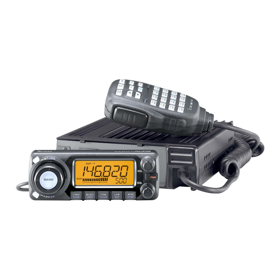
Icom IC-208H Service Manual
Vhf/uhf fm transceiver
Hide thumbs
Also See for IC-208H:
- Instruction manual (96 pages) ,
- Service manual (8 pages) ,
- Adjustment procedure (12 pages)
Table of Contents
Advertisement
Advertisement
Table of Contents

Related Manuals for Icom IC-208H


Summary of Contents for Icom IC-208H
- Page 1 SERVICE MANUAL VHF/UHF FM TRANSCEIVER i208H...
- Page 2 This service manual describes the latest service information NEVER connect the transceiver to an AC outlet or to a DC for the IC-208H VHF/UHF FM TRANSCEIVER at the time at power supply that uses more than 16 V. This will ruin the transceiver.
-
Page 3: Table Of Contents
TABLE OF CONTENTS SECTION 1 SPECIFICATIONS SECTION 2 INSIDE VIEWS SECTION 3 DISASSEMBLY INSTRUCTIONS SECTION 4 CIRCUIT DESCRIPTION 4 - 1 RECEIVER CIRCUITS ............4 - 1 4 - 2 TRANSMITTER CIRCUITS . -
Page 4: Specifications
SECTION 1 SPECIFICATIONS GENERAL • Frequency range VERSION RX (MHz) TX (MHz) [KOR] 144.000–146.000, 430.000–440.000 144.000–146.000* , 430.000–440.000 118.000–173.995* , 230.000–549.995* [USA] 810.000–824.000* , 849.000–869.000* 144.000–148.000, 420.000–450.000* 894.000–999.990* 118–173.995* , 230.000–549.995* [AUS] 144.000–148.000, 420.000–450.000* 810.000–999.990* [TPE] 144.000–146.000, 430.000–432.000 144.000–146.000, 430.000–432.000 118–173.995* , 230.000–549.995* [EXP]... -
Page 5: Inside Views
SECTION 2 INSIDE VIEWS • CONTROL UNIT (TOP VIEW) LCD back light LCD back light (DS22: CV1074) (DS22: CV1074) Key back light Key back lights DS13-DS18,DS20: SML512MW DS13-DS18, DS20: SML512MW DS21: SML-020MYT DS21: SML-020MYT • MAIN UNIT (TOP VIEW) Ceramic band pass filter Ceramic bandpass filter FI1: CFWS450HT FI1: CFWS450HT... - Page 6 • CONTROL UNIT (BOTTOM VIEW) Color controller Color controller +8V regurator +8V regulator +5V regurator +5V regulator (Q6,Q7: 2SC4116) (Q6, Q7: 2SC4116) Q1: 2SC4116 Q1: 2SC4116 IC5: TA78L05F IC5: TA78L05F Q3: 2SA1734 Q3: 2SA1734 D4: MA8062 D4: MA8062 D5: MA8068 D5: MA8068 Control unit CPU Control unit CPU...
-
Page 7: Disassembly Instructions
SECTION 3 DISASSEMBLY INSTRUCTIONS • Removing the MAIN unit Unscrew 8 screws G, and remove the MAIN unit. Unscrew 4 screws A, and remove the cover. Disconnect the cable B from J505, and remove the speaker. Remove 2 sheets c. MAIN UNIT J505 J505... - Page 8 • Removing the CONTROL unit Unscrew 2 screws C, and remove the LCD plate. Remove 2 knobs A. Remove the CONTROL unit. CONTROL UNIT Unscrew 2 screws B, and remove the cover. 3 - 2...
-
Page 9: Circuit Description
SECTION 4 CIRCUIT DESCRIPTION 4-1 RECEIVER CIRCUITS The signals from the antenna switching circuit pass through the each attenuator circuit (for VHF is D49 and D50, for UHF 4-1-1 DUPLEXER CIRCUIT (MAIN UNIT) is D46 and D48, for SHF is D39). The transceiver has a duplexer (low-pass and high-pass fil- The D/A converter outputs “ATT”... - Page 10 • ABOVE 230 MHz RF CIRCUIT • UHF (430 MHz–440 MHz) 1ST MIXER CIRCUIT (230 MHz–550 MHz, EXCEPT 430 MHZ–440 MHz) The signals from the UHF RF circuit are mixed with the 1st The signals from the attenuator circuit pass through the tun- LO signal at the 1st mixer circuit (Q35) to produce a 46.05 able bandpass filter (D36, L37, L38, C242, C253, C261).
- Page 11 • IN CASE OF FM SIGNAL RECEIVING When the signal passes through the other low-pass filter The signal is then amplified at the limiter amplifier section (C52, C53, R46, R52), the filtered signal is applied to the (IC5, pin 5) and applied to the FM detector section (X2, IC5, MAIN CPU (IC505, pin 42) via the “WXALT”...
-
Page 12: Transmitter Circuits
The signal from the AM detector circuit (Q13) is detected at The signals are amplified at the buffer amplifier (IC3C, pins the AGC detector circuit (D19–D21). When receiving strong 9, 8), and are then applied to the D/A converter IC (IC4, pin signals, the detected voltage increases and the AGC voltage 13) to adjust modulation level. - Page 13 4-2-3 VHF DRIVE AMPLIFIER CIRCUIT 4-2-5 VHF APC CIRCUIT (MAIN UNIT) (MAIN UNIT) The APC circuit protects the power amplifier from a mis- matched output load and stabilises transmit output power. The drive amplifier circuit amplifies the VCO oscillating sig- nal to a level needed at the power amplifier.
-
Page 14: Pll Circuits
4-2-7 UHF DRIVE AMPLIFIER CIRCUIT When antenna impedance is mismatched, the detected volt- age exceeds the reference voltage. The output voltage of (MAIN UNIT) the APC amplifier (IC15, pin 1) controls the bias voltage of The RF signals from the low-pass filter (VCO board) pass the power module (IC14) to reduce the output power via the through the high-pass filter (L69, C119) and attenuator APC controller (IC15, D531). - Page 15 4-3-3 UHF LOOP (VCO BOARD AND MAIN UNIT) • WHILE RECEIVING UHF BAND OR 800 MHz BAND The oscillated signal at the U-VCO circuit is amplified at the The generated signal at the U-VCO (Q101, D100, D101) buffer amplifiers (Q102, Q103), and is then applied to the enters the PLL IC (MAIN unit;...
-
Page 16: Other Circuits
4-4 OTHER CIRCUITS 4-5-2 MAIN UNIT VOLTAGE LINES 4-4-1 SUB-CPU RESET CIRCUIT (CONTROL UNIT) Description Line IC2 is the reset voltage detecting circuit. The output voltage The voltage from the external power supply via from the +5 regulator circuit (IC5) is applied to the VDD ter- the W501 (OPC-465). -
Page 17: Port Allocations
(MAIN unit; IC505)–Continued 4-6 PORT ALLOCATIONS 4-6-1 MAIN CPU PORT ALLOCATIONS Port Description number name (MAIN UNIT; IC505) CLONE_IN Input port for the cloning signal. Port Outputs the data signal to the D/A Description number name DA_DATA CONVERTER (IC11, pin 17). Outputs the transmit mute signal. - Page 18 (MAIN unit; IC505)–Continued 4-6-3 FRONT CPU PORT ALLOCATIONS (CONTROL UNIT; IC6) Port Description number name Port Description Outputs the VCO circuit select signal. number name VCO_SHIFT High : The VCO circuit oscillates Input port for the [BAND] key. BAND 203.95–263.945 MHz signal. Low : The [BAND] key is pushed.
-
Page 19: Adjustment Procedures
SECTION 5 ADJUSTMENT PROCEDURES 5-1 PREPARATION Need to enter the adjustment mode, and the JIG calble as shown the page 5-2 is required when adjusting the IC-208H. I REQUIRED TEST EQUIPMENT EQUIPMENT GREDE AND RANGE EQUIPMENT GREDE AND RENGE Output voltage : 13.8 V DC... - Page 20 ‘ ‘ CONNECTIONS FM DEVIATION ATTENUATOR METER 50 dB or 60 dB RF POWER METER POWER SUPPLY 50 , 1 80 W 13.8 V, 20 A or more STANDARD SIGNAL GENERATOR 0.1 300 MHz 127 to 17 dBm (0.1 V to 32 mV) CAUTION! DO NOT transmit while an SSG is...
-
Page 21: Software Adjustments
5-2 SOFTWARE ADJUSTMENTS (TRANSMITTING) ADJUSTMENT ADJUSTMENT CONDITION OPERATION REFERENCE • Operating frequency : 445.0 MHz • Turn the [DIAL] to set to 445.0000 MHz. FREQUENCY • Loosely couple a frequency counter to the antenna • Push the [BAND] key. [Fr] connector on the rear panel. - Page 22 SOFTWARE ADJUSTMENTS (TRANSMITTING AND RECEIVING)–Continued ADJUSTMENT ADJUSTMENT CONDITION OPERATION FREQUENCY • Operating frequency : 144.0 MHz • Turn the [DIAL] to set to ±4.6 kHz. DEVIATION • Connect an audio generator to the [MIC] jack and set • Push the [BAND] key. (VHF band) : +20 dB [DE]...
- Page 23 SOFTWARE ADJUSTMENT (RECEIVING)–Continued ADJUSTMENT ADJUSTMENT CONDITION OPERATION TRACKING • Operating frequency : 400.1 MHz • Push the [BAND] key. (Middle2 • Connect an SSG to the antenna connector and set as band) Level : 1 µV* (–107 dBm) [Tr] Modulation : 1 kHz Deviation : ±...
- Page 24 SOFTWARE ADJUSTMENT (RECEIVING)–Continued ADJUSTMENT ADJUSTMENT CONDITION OPERATION SQUELCH • Operating frequency : 146.1 MHz • Push the [BAND] key. LEVEL • Connect an SSG to the antenna connector and set as (Wide) Level : 0.079 µV* (–129 dBm) [SqW] Modulation : 1 kHz Deviation : ±...
- Page 25 SOFTWARE ADJUSTMENT (RECEIVING)–Continued ADJUSTMENT ADJUSTMENT CONDITION OPERATION TEMP. • Operating frequency : 445.0 MHz •Turn the [DIAL] to set to “F9” on the display. CORRECTION • Receiving • Push the [BAND] key. <High power> (UHF –10˚C) [HP–] (UHF +60˚C) • Operating frequency : 445.0 MHz •Turn the [DIAL] to set to “07”...
-
Page 26: Parts List
SECTION 6 PARTS LIST [CONTROL UNIT] [CONTROL UNIT] ORDER ORDER DESCRIPTION DESCRIPTION 1110005780 S.IC S-80945CLMC-G7F-T2 6510023680 CONNECTOR 2633 FRONT CONNECTOR 1180000420 S.IC TA78L05F (TE12R) 1140011370 S.IC HD6433842RD36H (FX2633D) 5030002580 LCD L2-0736TAY DS13 5040002930 S.LED SML-512MW T86P 1530002690 S.TRANSISTOR 2SC4116-GR (TE85R) DS14 5040002930 S.LED SML-512MW T86P... -
Page 27: Vco Unit
[VCO UNIT] [VCO UNIT] ORDER ORDER DESCRIPTION DESCRIPTION ERJ3GEYJ 390 V (39 Ω) D106 1790001620 S.DIODE 1SV308 (TPL3) R122 7030003270 S.RESISTOR D107 1790001260 S.DIODE MA2S077-(TX) R123 7030003730 S.RESISTOR ERJ3GEYJ 274 V (270 kΩ) R124 7030003520 S.RESISTOR ERJ3GEYJ 472 V (4.7 kΩ) ERJ3GEYJ 470 V (47 Ω) [USA] only R125 7030003280 S.RESISTOR... -
Page 28: Main Unit
[VCO UNIT] [MAIN UNIT] ORDER ORDER DESCRIPTION DESCRIPTION C124 4030006980 S.CERAMIC C1608 CH 1H 070D-T 1530002850 S.TRANSISTOR 2SC4116-BL (TE85R) C125 4030006860 S.CERAMIC C1608 JB 1H 102K-T 1590001190 S.TRANSISTOR XP6501-(TX) .AB C126 4030006950 S.CERAMIC C1608 CH 1H 040C-T 1530002850 S.TRANSISTOR 2SC4116-BL (TE85R) C127 4030009520 S.CERAMIC C1608 CH 1H 020B-T... - Page 29 [MAIN UNIT] [MAIN UNIT] ORDER ORDER DESCRIPTION DESCRIPTION 1790000980 S.DIODE MA742 (TX) 6200010630 S.COIL LQW18AN8N2D00D 1750000610 S.VARICAP MA2SV0500L 6200005590 S.COIL ELJRE 2N7Z-F 1720000700 S.VARICAP 1SV305 (TPL3) 6200009890 S.COIL C2012C-82NG 1790001260 S.DIODE MA2S077-(TX) 6200010060 S.COIL AS080647-56N 1790001160 S.DIODE 1SS362 (TE85R) 6200010160 S.COIL AS080440-22N 1750000510 S.DIODE UM9401F...
- Page 30 [MAIN UNIT] [MAIN UNIT] ORDER ORDER DESCRIPTION DESCRIPTION 7030003680 S.RESISTOR ERJ3GEYJ 104 V (100 kΩ) R122 7030003500 S.RESISTOR ERJ3GEYJ 332 V (3.3 kΩ) 7030003700 S.RESISTOR ERJ3GEYJ 154 V (150 kΩ) R123 7030003500 S.RESISTOR ERJ3GEYJ 332 V (3.3 kΩ) 7030003720 S.RESISTOR ERJ3GEYJ 224 V (220 kΩ) R124 7030003440 S.RESISTOR...
- Page 31 [MAIN UNIT] [MAIN UNIT] ORDER ORDER DESCRIPTION DESCRIPTION R212 7030003720 S.RESISTOR ERJ3GEYJ 224 V (220 kΩ) R537 7030003520 S.RESISTOR ERJ3GEYJ 472 V (4.7 kΩ) R213 7030003440 S.RESISTOR ERJ3GEYJ 102 V (1 kΩ) R538 7030003620 S.RESISTOR ERJ3GEYJ 333 V (33 kΩ) ERJ3GEYJ 221 V (220 Ω) R214 7030003360 S.RESISTOR...
- Page 32 [MAIN UNIT] [MAIN UNIT] ORDER ORDER DESCRIPTION DESCRIPTION R621 7030003640 S.RESISTOR ERJ3GEYJ 473 V (47 kΩ) 4030011600 S.CERAMIC C1608 JB 1E 104K-T R622 7030003660 S.RESISTOR ERJ3GEYJ 683 V (68 kΩ) 4030007020 S.CERAMIC C1608 CH 1H 120J-T R623 7030003680 S.RESISTOR ERJ3GEYJ 104 V (100 kΩ) 4030006940 S.CERAMIC C1608 CH 1H 030C-T R624...
- Page 33 [MAIN UNIT] [MAIN UNIT] ORDER ORDER DESCRIPTION DESCRIPTION C143 4030006860 S.CERAMIC C1608 JB 1H 102K-T C233 4030011140 S.CERAMIC GRM31M2C2H120JV01L (GRM42-6 CH) C144 4030006860 S.CERAMIC C1608 JB 1H 102K-T C234 4030006860 S.CERAMIC C1608 JB 1H 102K-T C145 4030007090 S.CERAMIC C1608 CH 1H 470J-T C235 4030006860 S.CERAMIC C1608 JB 1H 102K-T...
- Page 34 [MAIN UNIT] [MAIN UNIT] ORDER ORDER DESCRIPTION DESCRIPTION C512 4030006860 S.CERAMIC C1608 JB 1H 102K-T C602 4030006860 S.CERAMIC C1608 JB 1H 102K-T C513 4030011600 S.CERAMIC C1608 JB 1E 104K-T C603 4030006860 S.CERAMIC C1608 JB 1H 102K-T C514 4030009910 S.CERAMIC C1608 CH 1H 040B-T C604 4030006860 S.CERAMIC C1608 JB 1H 102K-T...
- Page 35 [MAIN UNIT] ORDER DESCRIPTION W506 7030000010 S.JUMPER MCR10EZHJ JPW (000) W507 7030003860 S.JUMPER ERJ3GE JPW V W508 7030003860 S.JUMPER ERJ3GE JPW V W509 7030000010 S.JUMPER MCR10EZHJ JPW (000) W510 7030003860 S.JUMPER ERJ3GE JPW V W511 7030003860 S.JUMPER ERJ3GE JPW V W512 7030003860 S.JUMPER ERJ3GE JPW V...
- Page 36 SECTION 7 MECHANICAL PARTS AND DISASSEMBLY [CHASSIS PART] [MAIN UNIT] REF. ORDER REF. ORDER DESCRIPTION QTY. DESCRIPTION QTY. 6510004880 Connector MR-DS-E 01 J502 6510023110 Connector 3008L-8P8C J503 6510019321 1729 rear connector-1 2510001160 Speaker 057P0802 J504 6510023160 Connector DN-508B-6 2710000760 Fan FD1240107B-1N J506 6510023590 Connector HSJ2000-01-010...
- Page 37 J1 (C) MP6 (C) MP11 (C) MP1 (C) MP17 (C) MP4 (C) MP10 (C) MP3 (C) MP12 (C) MF1(C) MP2 (CT) MP21(C) CONTROL UNIT MP25 (CT) MP26 (CT) MP1 (M) DS22 (CT) MP19 (C) MP20 (C) MP10 (M) MP18 (CT) MP8 (M) MP21 (CT)
- Page 38 SECTION 8 SEMI-CONDUCTOR INFORMATION • TRANSISTORS AND FET’S • DIODES 2SA1362 GR 2SA1586 GR 2SA1588 GR 2SA1734 2SB1182 TL Q 1SS355 1SS362 1SS400 1SV286 1SV305 (Symbol: AEG) (Symbol: SG) (Symbol: ZG) (Symbol: LB) (Symbol: None) (Symbol: A) (Symbol: C3) (Symbol: A) (Symbol: T7) (Symbol: TV) 2SC2954 T1...
- Page 39 SECTION 9 BOARD LAYOUTS 9-1 CONTROL UNIT • TOP VIEW LOCK BAND S.MW V/MHz M/CALL TONE MONI SCAN PRIO T-SCAN DTMF 9 - 1...
- Page 40 • BOTTOM VIEW (CONTROL UNIT) to MAIN unit J503 9 - 2...
- Page 41 9-2 MAIN UNIT • TOP VIEW J504 AFOUT PTTP DATAIN J502 MICIN PSQL DATAOUT MICE EXTMIC MICU/D J505 to Microphone to Speaker to VCO board J1 CHASSIS W501 BLACK to FAN to VCO board J2 J503 CTHV TXDATA RDATA to CONTROL unit CHASSIS 9 - 3...
- Page 42 • BOTTOM VIEW (MAIN UNIT) IC13 IC14 9 - 4...
-
Page 43: Vco Board
9-3 VCO BOARD • TOP VIEW * Mounted R127 in place of W1 ([USA], [E208] only) 9 - 5... - Page 44 • BOTTOM VIEW (VCO BOARD) V_LV V_VCO8 V_TXLO VCO_SHIFT V_RXLO U_LV U_TXLO U_RXLO MMUTE U_VCO8 800R5 PLLOUT to MAIN unit to MAIN unit *Mounted R128 in place of W2 ([USA], [E208] only) 9 - 6...
-
Page 45: Block Diagram
SECTION 10 BLOCK DIAGRAM ANTENNA MAIN UNIT VCO BOARD V VCO8 V_T8 D45 UM9401F D49 HVU131TRF IC1 MB15A02PFV-1 Q3 2SC5231 D50 UM9401F Q6 UMG9N D2 1SS400 D5 1SV308 T_UHF D2,D3 MA2S304 D47 1SS400 Q8 XP1115 D525 1SS400 2SC5231 D6 MA2S077 (430-450MHz) D1 1SV286 VCO8... -
Page 46: Voltage Diagrams
SECTION 11 VOLTAGE DIAGRAMS 11-1 CONTROL UNIT DS1 L2-0736TAY JRS0000-1401 DIAL-A DIAL-B 0.0047 R24 4.7k R25 10k SEG34 SEG8 P91/SEG34 P57/WKP7/SEG8 0.0047 SEG35 SEG7 P92/SEG35 P56/WKP6/SEG7 SEG36 SEG6 P93/SEG36 P55/WKP5/SEG6 SEG5 P94/SEG37/M P54/WKP4/SEG5 SEG4 S3-S11 P95/SEG38/DO P53/WKP3/SEG4 SKQDPA SEG3 P96/SEG39/CL2 P52/WKP2/SEG3 SEG2 P97/SEG40/CL1... -
Page 47: Main Unit
11-2 MAIN UNIT MAIN UNIT (1) BUS LINE1 HV_I HV_I HV_I ZBFS5101-PT 7.9V W548 5VS_W 5VS_W 5VS_W Q501 13.7V 2SB1182 PLLSW IC504 W501 R508 TA7808F MICMUTE D523 MA742 RX: 4.8V ZBFS5101-PT CLONE_IN EP528 TX: 4.8V D507 D511 D519 Q502 Q510 13.8V MATORIX_IN1 UNR9210J... - Page 48 MAIN UNIT (2) BUS LINE1 BUS LINE1 HV_I HV_I HV_I HV_I HV_I 5VS_W 5VS_W 5VS_W 5VS_W 5VS_W 1SV308 V_TXLO V_TXLO V_LV V_LV V_RXLO V_RXLO V_VCO8 V_VCO8 0.001 VCO_SHIFT VCO_SHIFT 7.1V U_TXLO U_TXLO U_LV U_LV U_RXLO U_RXLO 100k 0.5p MA2S077 MMUTE MMUTE MMUTE 800R5...
- Page 49 MAIN UNIT (3) BUS LINE1 BUS LINE1 HV_I HV_I HV_I HV_I HV_I 5VS_W 5VS_W 5VS_W 5VS_W 5VS_W R109 IC10 180k 0.01 TC4W53FU CFWS450HT TC4W53FU EP526 0.001 0.82 0.22 2SC4116 2SC4215 CFWM450E 100k 1.5k 470k XP4601 0.001 5VS_W 1.2k 100k R120 R119 DTCS_IN 470p...
- Page 50 MAIN UNIT (4) BUS LINE1 HV_I 5VS_W 5VS_W 5VS_W 5VS_W W529 W531 W533 W535 W537 W539 W541 W543 V_RXLO W530 W532 W534 W536 W538 W540 W542 RX: 4.3V TX: 0V R199 R147 RX: 3.9V Q515 Q516 TX: 0V W544 W545 C2012C-68NG DAN222 UNR9114J...
- Page 52 S-14001HZ-C1 1-1-32, Kamiminami, Hirano-ku, Osaka 547-0003, Japan C 2003 Icom Inc.
Need help?
Do you have a question about the IC-208H and is the answer not in the manual?
Questions and answers