Samsung MAX-G55 Service Manual
Dvd mini component system with usb host
Hide thumbs
Also See for MAX-G55:
- User manual (26 pages) ,
- Service manual (73 pages) ,
- Service manual (62 pages)
Table of Contents
Advertisement
Quick Links
SERVICE
DVD MINI COMPONENT SYSTEM WITH USB HOST
MAX-G55
Refer to the service manual in the GSPN (see the rear cover) for the more information.
DVD MINI COMPONENT
SYSTEM WITH USB HOST
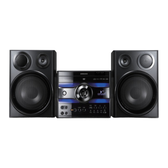
Model Name : MAX-G55
Model Code : MAX-G55R/EDC
Manual
1. Precaution
2. Product Specification
3. Disassembly & Reassembly
4. Troubleshooting
5. Exploded View & Part List
6. PCB Diagram
7. Schematic Diagram
CONTENTS
Advertisement
Chapters
Table of Contents

Related Manuals for Samsung MAX-G55


Summary of Contents for Samsung MAX-G55
- Page 1 DVD MINI COMPONENT SYSTEM WITH USB HOST Model Name : MAX-G55 Model Code : MAX-G55R/EDC SERVICE Manual DVD MINI COMPONENT SYSTEM WITH USB HOST CONTENTS 1. Precaution 2. Product Specification 3. Disassembly & Reassembly 4. Troubleshooting 5. Exploded View & Part List 6.
- Page 2 Asia asia.samsungportal.com Mideast & Africa mea.samsungportal.com © Samsung Electronics Co.,Ltd. May. 2009 This Service Manual is a property of Samsung Electronics Printed in Korea Co.,Ltd. Any unauthorized use of Manual can be punished under applicable International and/or domestic law.
-
Page 3: Table Of Contents
Contents 1. Precaution 1-1 Safety Precautions ................... 1-1 1-2 Servicing Precautions ..................1-3 1-3 Precautions for Electrostatically Sensitive Devices (ESDs) ......1-4 2. Product Specification 2-1 Product Feature ....................2-1 2-2 Specifications ....................2-4 2-3 Specifications Analysis ..................2-7 2-4 Accessories ......................2-9 3. Disassembly & Reassembly 3-1 Overall Disassembly &... - Page 4 Contents 7. Schematic Diagram 7-1 Overall Block Diagram ..................7-2 7-2 FRONT ......................7-3 7-3 MAIN ........................7-4 7-4 AMP .........................7-5 7-5 USB/MIC, MPEG Power ..................7-6 7-6 MPEG.......................7-7...
-
Page 5: Precaution
1 and 5.2 megohms. If there is no return path, the measured resistance should be “infinite.” If the resistance is outside these limits, a shock hazard might exist. See Fig. 1-2. Samsung Electronics... - Page 6 . Use replacement components that have the same ratings, especially for flame resistance and dielectric strength specifications. A replacement part that does not have the same safety characteristics as the original might create shock, fire or other hazards. Samsung Electronics...
-
Page 7: Servicing Precautions
8. Always connect a test instrument’s ground lead to the instrument chassis ground before connecting the positive lead; always remove the instrument’s ground lead last. First read the “Safety Precautions” section of this manual. If some unforeseen circumstance creates a conflict between the servicing and safety precautions, always follow the safety precautions. Samsung Electronics... -
Page 8: Precautions For Electrostatically Sensitive Devices (Esds)
9. Minimize body motions when handing unpackaged replacement ESDs. Motions such as brushing clothes together, or lifting a foot from a carpeted floor can generate enough static electricity to damage an ESD. Samsung Electronics... -
Page 9: Product Specification
• CD Ripping (1x, 192 Kbps) • Party Mode: Superb Sound + Flash LED Light Connectivity • USB Host (MP3) • Portable Audio In (3.5 phi Stereo Jack) Disc • Type: 3 Roulette • Compatible: MP3, CD-R/CD-RW, WMA Samsung Electronics... - Page 10 Product Specification 2-1-3 MAX-G55 Product Feature Power • 2ch: 180W Total RMS / 2,000W PMPO (Front: 90W/ch) • EQ: 6 Mode Special Functions • CD Ripping (1x, 192 Kbps) • Party Mode: Superb Sound + Flash LED Light Connectivity • USB Host (MP3) •...
- Page 11 • Portable Audio In (3.5 phi Stereo Jack) Disc • Type: 3 Roulette • Compatible: CD-R/CD-RW, WMA Disc • Type: 3 Roulette • Compatible: DVD, Divx, MP3, CD/CD-R/CD-RW, WMA, VCD (Regional Option) In/Out: Component, Composite, Audio L-R 2 Tape Deck Samsung Electronics...
-
Page 12: Specifications
90 Watts/CH RMS, IEC (total harmonic distortion: 10 %) Subwoofer Speaker (6Ω) 100 Watts/CH RMS, IEC (total harmonic distortion: 10 %) AMPLIFIER Output Power Channel separation 40 dB Signal/noise ratio 75 dB Power Consumption GENERAL Dimensions 377 (W) x 227 (H) x 270 (D) mm Samsung Electronics... - Page 13 Product Specification 2-2-2 MAX-G56 / MAX-G55 Specifications Basic Specification Signal/noise ratio 62 dB Usable sensitivity 10 dB RADIO FM Total harmonic 0.3 % distortion Capacity 3 discs Frequency range 20 Hz - 20 KHz (± 1 dB) COMPACT Signal/noise ratio 90 dB (at 1 KHz) with filter...
- Page 14 Front Speaker (6Ω) (MAX-DG54/DG53) 100 Watts/CH RMS, IEC (total harmonic distortion: 10 %) AMPLIFIER Subwoofer Speaker (6Ω) (MAX-DG54) Output Power Channel separation 60 dB Signal/noise ratio 70 dB Power Consumption 50 W GENERAL Dimensions 377 (D) x 227 (H) x 270 (W) mm Samsung Electronics...
-
Page 15: Specifications Analysis
HEADPHONE/MIC Karaoke Tuner Memory 57 Key Remote Key 60 Key 60 Key 40 Key Dual Voltage 4Ω SPK Impedance 4Ω 4Ω 4Ω : application, X: non-application Samsung Electronics... - Page 16 Product Specification MAX-DA55 Model Name MAX-DG55 MAX-G55 MAX-DG54 MAX-DG53 Photo 180W 180W 180W 280W 180W 90W x 2 + 90W x 2 Output Power 90W x 2 90W x 2 90W x 2 100W Front Display Party Mode DIMMER ...
-
Page 17: Accessories
Product Specification 2-4 Accessories 2-4-1 Supplied Accessories Accessories Item Item code Remark AH59-02147A Remote Control Samsung Service AH42-00021A FM Antenna Center AH68-02162F AH68-02162G User's Manual AH68-02162H Samsung Electronics... - Page 18 MEMO 2-10 Samsung Electronics...
-
Page 19: Disassembly & Reassembly
IC chips on the PCB are vulnerable to static electricity. - Assemble in the reverse order of disassembly. Part Name Description Description Photo COVER- 1) Unfasten 15 screws. SIDE-L : BH,3*10,BLACK COVER- Be careful not to make any SIDE-R scratches as you remove it. CABINET- REAR <MAX-DG56 CABINET-REAR> Samsung Electronics... - Page 20 Disassembly & Reassembly Part Name Description Description Photo COVER- SIDE-L COVER- SIDE-R CABINET- REAR <MAX-G55 CABINET-REAR> <MAX-G56/DG55 CABINET-REAR> <MAX-DG54/DG53 CABINET-REAR> Samsung Electronics...
- Page 21 1) Pull up and remove the CABINET- TOP. DOOR-CD 2) Power on and open the disk, separate DOOR-CD. CD-DECK 1) Pull up and remove the CD-DECK. MPEG PCB 1) Unfasten the 3 screws and remove (MAX-DG5x MPEG PCB. Only) : BH 2.6*8 WHITE Samsung Electronics...
- Page 22 Disassembly & Reassembly Part Name Description Description Photo CABINET- 1) Unfasten the 6 screws and remove REAR CABINET-REAR. : BH,3*10,BLACK <MAX-DG56 CABINET-REAR> <MAX-G55 CABINET-REAR> <MAX--G56/DG55 CABINET-REAR> <MAX-DG54/DG53 CABINET-REAR> Samsung Electronics...
- Page 23 Disassembly & Reassembly Part Name Description Description Photo MAIN PCB 1) Unfasten 8 screws on the MAIN-PCB. : BH,3*10,WHITE CABINET 1) Unfasten the 2 screws. BOTTOM : BH,3*10,black Samsung Electronics...
- Page 24 1) Pull the hook at 1 and 2 of and FRONT separate ASSY-FRONT. TAPE DECK 2) (MAX-DG54/DG53 Only) 4 screws to disasemble tape deck. : BH 3*10 BLACK <MAX-DG54/DG53 TAPE-DECK> 3) Unfasten 11 screws. : BH 3*10 BLACK <MAX-DG56/G56/DG55/G55 ASSY FRONT> <MAX-DG54/DG53 ASSY FRONT> Samsung Electronics...
-
Page 25: Troubleshooting
Troubleshooting 4. Troubleshooting 4-1 Checkpoints by Error Mode ..............4-2 4-2 MICOM, MPEG Initialization & Update ..........4-11 Samsung Electronics... -
Page 26: Checkpoints By Error Mode
MAIN PCB FCN1 VFD-: Pin 7, -VP: Pin 10) Pin 26, 27, 28. Check reset circuit in Replace X-TAL1, UQ1 parts MAIN PCB X-TAL1, UQ1 part ok? Refer to wave pattern image of Fig. 4-2. Replace MICOM IC Samsung Electronics... - Page 27 Troubleshooting MAIN, page 7-4 UIC1 MAIN PCB Bottom, page 6-8 <Fig. 4-1> Samsung Electronics...
- Page 28 Troubleshooting FIC1 MAIN, page 7-4 UIC1 DCN1 MAIN PCB Bottom, page 6-8 <Fig. 4-2> Samsung Electronics...
- Page 29 FIC1 Pin 24: 9V Refer to wave pattern image of Fig. 4-3-1 and Fig. 4-3-2. Check MAIN PCB Check SMPS stage PT01 Pin 9: -24V and (All power source check) Pin 11: +24V Replace AAIC1 (L/R), AAIC2 (Subwoofer) Samsung Electronics...
- Page 30 Troubleshooting DCN1 AMP, page 7-5 AAIC1 AAIC2 MAIN PCB Top, page 6-6 <Fig. 4-3-1> Samsung Electronics...
- Page 31 Troubleshooting MAIN, page 7-4 FIC1 MAIN PCB Bottom, page 6-8 HIC1 <Fig. 4-3-2> Samsung Electronics...
- Page 32 “NO DISC” after Check Pick up Lens Loading a long time? and Pick up Flat Cable Check MIC1 ZR36966 Check Servo Parts Check DCN1 Pin 19, 20, 21 and 22 Refer to wave pattern image of Fig. 4-5. Samsung Electronics...
- Page 33 Troubleshooting MIC3C MIC3D OPIC1 MPEG, page 7-7 BIC1 MIC1 DIC1 RFCON1 MPEG PCB Top, page 6-10 <Fig. 4-4> Samsung Electronics...
- Page 34 Troubleshooting MAIN, page 7-4 DCN1 MAIN PCB Top, page 6-6 <Fig. 4-5> 4-10 Samsung Electronics...
-
Page 35: Micom, Mpeg Initialization & Update
3. DVD Model: Osd shows update screen. You have to make sure your update file is most recently version. Then press “ENTER” to proceed. CD Model: VFD shows “reading”. And “update” shows up and blinking. Wait until MAIN set automatically power off. Samsung Electronics 4-11... - Page 36 MEMO 4-12 Samsung Electronics...
-
Page 37: Exploded View & Part List
Exploded View & Part List 5. Exploded View & Part List 5-1 Exploded View ..................5-2 5-2 Speaker System..................5-4 5-3 Electrical Part List ................5-5 Samsung Electronics This Document can not be used without Samsung’s authorization. -
Page 38: Exploded View
Exploded View & Part List 5-1 Exploded View S.N.A: Service Not Available This Document can not be used without Samsung’s authorization. Samsung Electronics... - Page 39 T0002 AH64-04873A CABINET-BOTTOM;MAX-G55,SECC 0.8,262,298 T0003 AH64-04844A CABINET-FRONT;MAX-G55,HIPS,264,226 T0023 AH64-04847A KNOB-POWER;MAX-G55,ABS,28,28 T0245 AH61-02903A HOLDER-PCB;MAX-G55,ABS,25,40,BLK T0268 AC39-10019A CBF-POWER CORD;KKP-419C,H03VVH2-F,VDE/KE W004 6003-000283 SCREW-TAPTYPE;BH,+,-,B,M3,L8,ZPC(WHT),SW W384 6002-000126 SCREW-TAPPING;FH,+,-,2S,M3,L10,ZPC(BLK), W391 6003-000275 SCREW-TAPTYPE;BH,+,B,M3,L10,ZPC(BLK),SWR WA003 AH66-00303A WIRE-CLAMP;MAX-G55,NYLON,L24,BLK Samsung Electronics This Document can not be used without Samsung’s authorization.
-
Page 40: Speaker System
IMPEDANCE 4Ω FRONT FRONT Front Speaker (R) Part List Loc. No. Code No. Description;Specification Q’ty SNA Remark Front Speaker (L) AH81-04703A SPEAKER; PS-G55,SPEAKER SYSTEM _L-,-,-,-,- Front Speaker (R) AH81-04702A SPEAKER; PS-G55,SPEAKER SYSTEM _R,-,-,-,-,- This Document can not be used without Samsung’s authorization. Samsung Electronics... -
Page 41: Electrical Part List
SA AH66-00237A LEVER-SIDE;SDM-R31,POM (F20-03) SA RIC3 1003-001508 IC-MOTOR DRIVER;FAN8082DTF,SOP,8P,2 SA AH66-00238A CAM-SLIDER;SDM-R31,POM (F20-03) SA RR17 2007-001146 R-CHIP;7.5ohm,5%,1/8W,TP,2012 SNA RR2 2007-000075 R-CHIP;220ohm,5%,1/10W,TP,1608 SNA AH66-10008A PULLEY-MOTOR;POM,BLK,CMS-CR3 SA AH97-02666A ASSY-TRAVERSE;CMS-S78RB,DVD DECK,FI SNA SD3 0407-000114 DIODE-SWITCHING;KDS184,80V,100mA,SO SA Samsung Electronics This Document can not be used without Samsung’s authorization. - Page 42 3811-001868 WIRE-NO SHEATH CU;SnCuFe,52mm,GRY 189 SNA KAC5 2203-001126 C-CER,CHIP;0.68nF,10%,50V,X7R,1608 SNA AR61 2007-000869 R-CHIP;4.7Kohm,1%,1/10W,TP,1608 SA KAR11 2007-000124 R-CHIP;2.2Kohm,5%,1/10W,TP,1608 14 SNA ARR2 2007-000102 R-CHIP;100Kohm,5%,1/10W,TP,1608 12 SNA BD707 3301-000297 BEAD-AXIAL;25ohm,3.6x1.2x5.7mm,-,TP SNA KAR21 2007-000070 R-CHIP;0ohm,5%,1/10W,TP,1608 SNA This Document can not be used without Samsung’s authorization. Samsung Electronics...
- Page 43 SNA 0403-000149 DIODE-ZENER;1N4742A,5%,1000MW,DO-41 SA R1SS35 2004-000459 R-METAL;2.2Kohm,1%,1/8W,AA,TP,1.8x3 SNA R227 2007-000086 R-CHIP;5.6Kohm,5%,1/10W,TP,1608 SNA 0403-001062 DIODE-ZENER;UDZSNP4.7B,4.55/4.75V,2 SA R2D8 2001-000613 R-CARBON;3.9Kohm,5%,1/8W,AA,TP,1.8x SNA 0406-001128 DIODE-TVS;MLVS-0603-E08,50V SA R320 2007-000458 R-CHIP;18Kohm,5%,1/10W,TP,1608 SNA 1203-004564 IC-DC/DC CONVERTER;AP1501A,TO-220(R SNA Samsung Electronics This Document can not be used without Samsung’s authorization.
- Page 44 SNA C610 2202-002037 C-CERAMIC,MLC-AXIAL;100nF,+80-20%,5 SNA C661 2202-002055 C-CERAMIC,MLC-AXIAL;47nF,+80-20%,50 SNA CER04 2007-000084 R-CHIP;4.7Kohm,5%,1/10W,TP,1608 SNA D0254 0609-001352 MODULE REMOCON;HORIZONTAL,20mm,TR SNA EMC10 2401-000487 C-AL;10uF,20%,50V,GP,TP,6.3x5mm,5 SNA FAC11 2401-000651 C-AL;2.2uF,20%,50V,GP,TP,4x7,5 SA FAN1 3711-000820 HEADER-BOARD TO CABLE;BOX,2P,1R,2.5 SA This Document can not be used without Samsung’s authorization. Samsung Electronics...
-
Page 45: Pcb Diagram
PCB Diagram 6. PCB Diagram 6-1 Wiring Diagram....................6-2 6-2 FRONT PCB Top ....................6-3 6-3 FRONT PCB Bottom ..................6-5 6-4 MAIN PCB Top ....................6-6 6-5 MAIN PCB Bottom .................... 6-8 6-6 MPEG PCB Top ....................6-10 6-7 MPEG PCB Bottom ..................6-13 Samsung Electronics... -
Page 46: Wiring Diagram
AUX JACK op/cl) MIC JACK/PRE-AMP/ECHO USB JACK (sled) 17P (CTRL+EQ) 12P (power_supply) 28P (AUDIO SIGNAL, MPEG CTRL) MAIN PCB SMPS BLOCK AMPLIFIER FUNCTION/EQ SPK JACK TUNER PACK MICOM 30P (KEY, VFD) FRONT PCB VFD DISPLAY REMOTE EYE VFD DRIVER Samsung Electronics... -
Page 47: Front Pcb Top
PCB Diagram 6-2 FRONT PCB Top UCW1 Samsung Electronics... - Page 48 PCB Diagram 6-2-1 Pin Connection 1 UCW1 Front PCB (Control VFD, KEY) Pin No. Signal VFDGND VFDGND VFD+ VFD- 5.6V REMOCON CD-KEY VOL-DOWN VOL-UP KEY2 LED8 LED7 LED6 LED5 VFD_DO VFD_DI VFD_CL VFD_CE AUX_SENSE AUX_R AUX_L HP_SENSE Samsung Electronics...
-
Page 49: Front Pcb Bottom
PCB Diagram 6-3 FRONT PCB Bottom UCW1 Samsung Electronics... -
Page 50: Main Pcb Top
PCB Diagram 6-4 MAIN PCB Top DCN1 AAIC1 AAIC2 1SIC01 Samsung Electronics... - Page 51 CVBS KEY2 DGND REC-R LED8 P_CHECK REC-L LED7 MIC_SCORE OUT-R LED6 I2CDATA LED5 I2CCLK OUT-L VFD_DO DAC CS VFD_DI MRST VFD_CL DVD_TXD VFD_CE DVD_ACK DVD_RXD AUX_SENSE DVD_STB AUX_R MODE_SW IN SW AUX_L OUT SW T-SENS OPEN_MOTOR CLOSE_MOTOR HP_SENSE Samsung Electronics...
-
Page 52: Main Pcb Bottom
PCB Diagram 6-5 MAIN PCB Bottom FIC1 EIC1 HIC1 UIC1 DCN1 BIC1 IC1P103 Samsung Electronics... - Page 53 PCB Diagram 6-5-1 Test Point Wave Form Samsung Electronics...
-
Page 54: Mpeg Pcb Top
PCB Diagram 6-6 MPEG PCB Top MIC3C PCON1 MIC3D OPIC1 PIC1 BIC1 MIC1 MIC2 DIC1 RFCON1 ACCON1 6-10 Samsung Electronics... - Page 55 MGND Pin No. Signal VGND CVBS MGND DGND MGND P_CHECK MIC_SCORE DGND I2CDATA 3.3V I2CCLK 3.3V DAC CS Vref DGND MRST DVD_TXD DVD-VR DVD_ACK DGND DVD_RXD DVD-LD DVD_STB RFCON1 MODE_SW H-Vcc IN SW OUT SW T-SENS OPEN_MOTOR CLOSE_MOTOR Samsung Electronics 6-11...
- Page 56 PCB Diagram 6-6-2 Test Point Wave Form 6-12 Samsung Electronics...
-
Page 57: Mpeg Pcb Bottom
PCB Diagram 6-7 MPEG PCB Bottom PCON1 MIC4 RFCON1 Samsung Electronics 6-13... - Page 58 MEMO 6-14 Samsung Electronics...
-
Page 59: Schematic Diagram
Schematic Diagram 7. Schematic Diagram 7-1 Overall Block Diagram ..................7-2 7-2 FRONT ....................... 7-3 7-3 MAIN ........................7-4 7-4 AMP ........................7-5 7-5 USB/MIC, MPEG Power ................... 7-6 7-6 MPEG ........................ 7-7 Samsung Electronics This Document can not be used without Samsung’s authorization. -
Page 60: Overall Block Diagram
CD/DVD SIGNAL BUFFER TUNER TUNER SINGNAL DAIC2 PACK 4560 TAPE SINGNAL TAPE HA12237F DECK TAPE EQ PWM POWER REC-IN STAGE MIC_MIX FUNCTION FIC1 AIC1 FIC1 TDA8920 OPTION LC75106 R2S15904S This Document can not be used without Samsung’s authorization. Samsung Electronics... -
Page 61: Front
Schematic Diagram 7-2 FRONT POWER AUDIO Samsung Electronics This Document can not be used without Samsung’s authorization. -
Page 62: Main
Schematic Diagram 7-3 MAIN POWER AUDIO VIDEO This Document can not be used without Samsung’s authorization. Samsung Electronics... -
Page 63: Amp
Schematic Diagram 7-4 AMP POWER AUDIO Samsung Electronics This Document can not be used without Samsung’s authorization. -
Page 64: Usb/Mic, Mpeg Power
Schematic Diagram 7-5 USB/MIC, MPEG Power POWER AUDIO This Document can not be used without Samsung’s authorization. Samsung Electronics... -
Page 65: Mpeg
Schematic Diagram 7-6 MPEG POWER AUDIO Samsung Electronics This Document can not be used without Samsung’s authorization. - Page 66 MEMO Samsung Electronics...
Need help?
Do you have a question about the MAX-G55 and is the answer not in the manual?
Questions and answers