Table of Contents
Advertisement
IPC@CHIP SC123/SC143
Hardware Manual V1.06 [18.02.2010]
©2000-2008 BECK IPC GmbH
Hardware Manual
IPC@CHIP Embedded Controller Family
SC123/SC143
High Performance, 80186-Compatible,
16-Bit Embedded Microcontroller
Single Chip PC with Flash, RAM, Watchdog
Order No. IPC@CHIP
Embedded Controller SC123:
Embedded Controller SC123-LF:
Embedded Controller SC123-IEC:
Embedded Controller SC123-IEC-LF:
Embedded Controller SC143:
Embedded Controller SC143-LF:
Embedded Controller SC143-IEC:
Embedded Controller SC143-IEC-LF:
541094
543257
541528
543259
541529
543258
541530
543260
Page 1
Advertisement
Table of Contents

Related Manuals for Beck IPC SC123


Summary of Contents for Beck IPC SC123
- Page 1 Order No. IPC@CHIP Embedded Controller SC123: 541094 Embedded Controller SC123-LF: 543257 Embedded Controller SC123-IEC: 541528 Embedded Controller SC123-IEC-LF: 543259 Embedded Controller SC143: 541529 Embedded Controller SC143-LF: 543258 Embedded Controller SC143-IEC: 541530 Embedded Controller SC143-IEC-LF: 543260 ©2000-2008 BECK IPC GmbH Page 1...
- Page 2 IPC@CHIP SC123/SC143 Hardware Manual V1.06 [18.02.2010] Copyright & Trademark IPC@CHIP® is a registered trademark of Beck IPC. Ethernet is a registered trademark of Xerox Corporation. All other product names, company names, logos or other designations mentioned herein are trademarks of their respective owners.
-
Page 3: Table Of Contents
SPI .............................. 33 I²C ............................... 35 CAN ............................36 6.5.1 Introduction ............................36 6.5.2 TX Channels ............................37 6.5.3 RX Channel ............................37 USB ............................. 38 Power Fail Interrupt ........................39 6.7.1 Description ............................. 39 ©2000-2008 BECK IPC GmbH Page 3... - Page 4 11.3 External memory ......................... 56 11.4 Traffic/Link/Speed LEDs ......................57 11.5 SC1x3 Socket ..........................58 11.6 Custom series programming of SC1x3 ..................58 CPUCLK handling ....................59 Reflow Profile ......................60 History ........................61 ©2000-2008 BECK IPC GmbH Page 4...
- Page 5 Figure 11-3: Example circuit for connecting an external memory .................. 56 Figure 11-4: Circuit Example for two bi-coloured LEDs ....................57 Figure 11-5: Circuit Example for four mono-coloured LEDs ..................57 Figure 11-6: SC1x3-Socket ............................58 Figure 13-1: Reflow Profile ............................60 ©2000-2008 BECK IPC GmbH Page 5...
- Page 6 Table 8-8: PHY Receiver Input Characteristics ......................46 Table 8-9: 100Base-TX Transceiver Characteristics ..................... 46 Table 8-10: AC Characteristics ............................47 Table 10-1: Package Dimensions ..........................52 Table 13-1: Typical Reflow Profile Conditions ....................... 60 ©2000-2008 BECK IPC GmbH Page 6...
-
Page 7: Overview
As an option it can also be used in combination with an IEC61131-3 CoDeSys Run Time System. IPC@CHIP FLASH CoDeSys license included SC123 8 MByte 2 MByte SC123-IEC 8 MByte 2 MByte SC143 8 MByte 8 MByte SC143-IEC 8 MByte 8 MByte ©2000-2008 BECK IPC GmbH Page 7... -
Page 8: Features
One Universal Serial Bus (USB) 1.1 Port Software-compatible with the 80C186 microcontrollers and IPC@CHIP family One 3-wire Serial Peripheral Interface (SPI) SC11/12/13 with widely available native controller (48MHz) development tools, applications, and system software One 2-wire I²C serial controller ©2000-2008 BECK IPC GmbH Page 8... -
Page 9: Block Diagram
TMRIN 1:0 I²C Timer Controller Controller TMROUT 1:0 PCS7:0, MCS0 INT 1,3,5# Interrupt Chip- Controller Select Unit UCSOUT#, FLSSEL SDI, SDO, SCK, UCSIN# FLASH Controller SLVSEL SDRAM ARDY System Interface Figure 3-1: Block Diagram ©2000-2008 BECK IPC GmbH Page 9... -
Page 10: Pin Description
IPC@CHIP SC123/SC143 Hardware Manual V1.06 [18.02.2010] Pin Description 4.1 Pin Configuration Figure 4-1: Ball Grid Array Looking through Top of Package DNC Do Not Connect ! ©2000-2008 BECK IPC GmbH Page 10... -
Page 11: System Interface
OUT [4mA] Reset Output (Active LOW) This pin indicates whether the CPU is being reset. It indicates that the internal logic is being reset and is to be used to reset any external peripherals. ©2000-2008 BECK IPC GmbH Page 11... -
Page 12: Table 4-1: Pin Description Of System Interface
These pins supply the address to memory or I/O of the system. A[20] A[19] A[18] A[17] A[16] A[15] A[14] A[13] A[12] A[11] A[10] A[9] A[8] A[7] A[6] A[5] A[4] A[3] A[2] A[1] Table 4-1: Pin Description of System Interface Note 1: 5V tolerant ©2000-2008 BECK IPC GmbH Page 12... -
Page 13: Chip Selects
This pin is for selecting external memory. If this pin is high, the internal flash is selected. When low, external memory can be accessed (E.g. see chapter 11.3). Table 4-2: Pin Description of Chip Selects Note 1: 5V tolerant ©2000-2008 BECK IPC GmbH Page 13... -
Page 14: Dma
Clear to Send 0 In (Schmitt Trigger Input, Active High with Pull up) CTS0# This pin provides the Clear to Send input for serial port 0. This pin provides the handshaking input for serial port 0. Table 4-5: Pin Description of UART0 Note 1: 5V tolerant ©2000-2008 BECK IPC GmbH Page 14... -
Page 15: Uart1 Interface
Clear to Send 2 In (Schmitt Input with Pull-up) PIO21 I/O [4mA] CTS2# This pin can be used with UART 2 as Clear to Send (CTS2#). It can also be used as PIO[21]. Table 4-7: Pin Description of UART2 ©2000-2008 BECK IPC GmbH Page 15... -
Page 16: I²C Bus
PIO bit [24] must be programmed for PIO operation. Programmable Input/Output PIO26 I/O [4mA] PIO bit [26] must be programmed for PIO operation. Table 4-9: Pin Description of Pure PIO pins Note 1: 5V tolerant ©2000-2008 BECK IPC GmbH Page 16... -
Page 17: Spi Bus / Uart3
PIO1 I/O [4mA] TMR1OUT OUT [4mA] This pin can be used with Timer Channel 1 as TMR1OUT. It can also be used as PIO[1]. Table 4-11: Pin Description of Timers Note 1: 5V tolerant ©2000-2008 BECK IPC GmbH Page 17... -
Page 18: Can Bus Interface
TEST pin (Schmitt Trigger Input and Pull-up) When this pin is pulled LOW, internal test modes may be input using address line 1 to 7. When HIGH, test is disabled. Table 4-14: Pin Description of JTAG Note 1: 5V tolerant ©2000-2008 BECK IPC GmbH Page 18... -
Page 19: Ethernet 0 Interface (Internal Phy)
Ethernet Receive Data Bus Bit [2] RXD[1] Ethernet Receive Data Bus Bit [1] RXD[0] Ethernet Receive Data Bus Bit [0] Ethernet Receive Carrier Sense RXCRS Ethernet Receive Collision RXCOL Table 4-16: Pin Description of MII Note 1: 5V tolerant ©2000-2008 BECK IPC GmbH Page 19... -
Page 20: Phy Power (Internal Phy)
Power I/O: +3.3 volt power supply Power I/O: +3.3 volt power supply Power I/O: +3.3 volt power supply Power I/O: +3.3 volt power supply Power I/O: +3.3 volt power supply Table 4-18: Pin Description of Power Pins ©2000-2008 BECK IPC GmbH Page 20... -
Page 21: Programmable I/O Pins
Shared Function Name TMRIN1 TMROUT1 PCS[6]# PCS[5]# PCS[4]# PCS[7]# ARDY DRQ2 DRQ3 TMROUT0 TMRIN0 DRQ0 I2CDTA CAN1TXD CAN1RXD CTS3#/SLVSEL# RTS3#/SCK RTS2# CTS2# TXD2 RXD2 TXD3/SD0 RXD3/SDI DRQ1 INT5# I2CCLK Table 4-19: List of PIO sharing designations. ©2000-2008 BECK IPC GmbH Page 21... -
Page 22: System Start-Up Configuration
9..1] pull-down device. internal pull-down can also configured by software through RTOS API these resistors are only necessary, if any device is connected to these pins The external resistors should have 10 K . ©2000-2008 BECK IPC GmbH Page 22... -
Page 23: Pfi Pin
IPC@CHIP! power on CHIP.INI : [DEVICE] no (default) PFI_ENABLE = 1 PFI pin = low (default = high) boot up Figure 5-1: power on flowchart with power fail interrupt enabled ©2000-2008 BECK IPC GmbH Page 23... -
Page 24: Functional Description
Table 6-1: General Purpose Registers Code Segment Register Data Segment Register Stack Segment Register Extra Segment Register Segment Registers FLAGS Status Word Instruction Pointer Status and Control Registers Table 6-2: Segment, Status and Control Registers ©2000-2008 BECK IPC GmbH Page 24... -
Page 25: Memory Organization
Figure 6-1: 24-Bit Address Generation 6.1.3 24-Bit Address Mode Figure 6-2: Contiguously segments in memory The SC1x3 divides it’s address space into segments of 64k. Each segment overlaps 256 bytes to the next segment. ©2000-2008 BECK IPC GmbH Page 25... -
Page 26: Peripheral Accesses Through The Address-/Databus
, CSBE = 0, Read = 0x55 Word read from 0xC00 e.g. > I W C00 BHE# Address = 000C00 A22:0 1234 D15:0 PCS6# Figure 6-4: 16 Bit read access from C00 , CSBE = 0, Read = 0x1234 ©2000-2008 BECK IPC GmbH Page 26... -
Page 27: Figure 6-5: 16 Bit Read Access From C01 , Csbe = 0, Read = 0X5678
, CSBE = 0, Read = 0x5678 Byte read from 0xC01 e.g. > I B C01 BHE# Address = 000C01 A22:0 55xx D15:0 PCS6# Figure 6-6: 8 Bit read access from C01 , CSBE = 0, Read = 0x55 ©2000-2008 BECK IPC GmbH Page 27... -
Page 28: Figure 6-7: 8 Bit Write Access To C00 , Csbe = 0, Write = 0X23
, CSBE = 0, Write = 0x23 Word write to 0xC00 e.g. > OW C00 1234 BHE# Address = 000C00 A22:0 1234 D15:0 PCS6# Figure 6-8: 16 Bit write access to C00 , CSBE = 0, Write = 0x1234 ©2000-2008 BECK IPC GmbH Page 28... -
Page 29: Figure 6-9: 16 Bit Write Access To C01 , Csbe = 0, Write = 0X5678
0xC01 0xC00 Byte write to 0xC01 e.g. > OW C01 23 BHE# Address = 000C01 A22:0 2323 D15:0 PCS6# Figure 6-10: 8 Bit write access to C01 , CSBE = 0, Write = 0x23 ©2000-2008 BECK IPC GmbH Page 29... -
Page 30: Figure 6-11: 8 Bit Write Access To C00 , Csbe = 1, Write = 0X23
, CSBE = 1, Write = 0x23 Byte write to 0xC01 e.g. > OB C01 23 Address = 000C00 A22:1 2323 D15:0 PCS6# WRL# WRH# Figure 6-12: 8 Bit write access to C01 , CSBE = 1, Write = 0x23 ©2000-2008 BECK IPC GmbH Page 30... -
Page 31: Figure 6-13: 16 Bit Write Access To C00 , Csbe = 1, Write = 0X1234
> OW C01 5678 Address = 000C00 Address = 000C02 A22:1 7856 7856 D15:0 PCS6# WRL# WRH# Figure 6-14: 16 Bit write access to C01 , CSBE = 1, Write = 0x5678 Result: 0xC03 0xC02 0xC01 0xC00 ©2000-2008 BECK IPC GmbH Page 31... -
Page 32: Uarts
Double-buffered transmit and receive Programmable user call-back function for transmit and receive 6.2.1 RTOS Update via serial ports The RTOS version can be updated via UART0 (COM0) or UART1 (COM1), see chapter 5 System Start-up Configuration). ©2000-2008 BECK IPC GmbH Page 32... -
Page 33: Spi
Attention: The SC1x3 is not capable to receive or send continous with a clock rate of 1/16 CPU in slave mode. This would cause to heavy interrupt load and would lead into a system crash. The maximum clock frequency in master mode is 48MHz. ©2000-2008 BECK IPC GmbH Page 33... -
Page 34: Table 6-4:Context Between Sdo And Sdi To Mosi And Miso In Different Modes
For using the function Autodrive to automaticly drive the Slave Select SPI_ALTERNATE_IO has to be set (see RTOS API). The following table describes the context: SC1x3 SPI Master MOSI MISO SPI Slave MISO MOSI Table 6-4:Context between SDO and SDI to MOSI and MISO in different modes ©2000-2008 BECK IPC GmbH Page 34... - Page 35 Arbitration-lost interrupt with automatic mode switching from master to slave Calling address identification interrupt with automatic mode switching from master to slave START and STOP signal generation/detection Repeated START signal generation Acknowledge bit generation/detection Bus busy detection 100 kHz to 400 kHz operation ©2000-2008 BECK IPC GmbH Page 35...
-
Page 36: Can
The Run mode is the normal operating mode. The following table shows the provided baud rates: 10 KBit/s 20 KBit/s 50 KBit/s 125 KBit/s 250 KBit/s 500 KBit/s 1 MBit/s Table 6-5: Provided CAN baud rates ©2000-2008 BECK IPC GmbH Page 36... -
Page 37: Tx Channels
A hardware FIFO stores the last four incoming messages. Status flags indicate how many messages are stored. Additional flags determine the acceptance filter from which the actual message is coming. Message µP Bus CAN Bus Filters ©2000-2008 BECK IPC GmbH Page 37... -
Page 38: Usb
SC1x3 will initiate the attach event at the Host, before the SC1x3 USB driver is ready. SC1x3 is Device SC1x3 is Host 3.3V active tristate tristate active tristate active USBN USBP 3.3V SC1x3 HOSTMODE Figure 6-16: Pullup-/down Resistors for USB full-speed device ©2000-2008 BECK IPC GmbH Page 38... -
Page 39: Power Fail Interrupt
By mapping external memory to the internal RTOS architecture, any memory can be connected to the SC1x3. This allows the user to use an NV-SRAM, a battery buffered SRAM or any other device that can be mapped to the internal memory (see chapter 0) to save non-volatile data. ©2000-2008 BECK IPC GmbH Page 39... -
Page 40: Mapping External Memory
The second Ethernet controller (MAC1) is connected to interrupt 1 and is shared with the external interrupt 1. This Ethernet controller connects to an MII port (Media Independent Interface). The main function of this interface is to provide a communication path between the internal MAC and an external PHY. ©2000-2008 BECK IPC GmbH Page 40... -
Page 41: Timers
1.8V OK RSTOUT# Delay RSTOUT# WDOG# Figure 6-18: Internal reset processing Note: There is no internal observing mechanism for the 3.3V supply voltage. The supply voltage has to be observed from a external supervisory circuit. ©2000-2008 BECK IPC GmbH Page 41... -
Page 42: System Overview
2/8 MB Flash PCS6# (C00h-DFFh) Memory PCS5# (A00h-BFFh) 800000h 7FFFFFh PCS4# (800h-9FFh) MCS0# PCS3# (600h-7FFh) 8 MB SDRAM PCS2# (400h-5FFh) 040000h 03FFFFh LCS# PCS1# (200h-3FFh) 256 KB SRAM 000000h PCS0# (000h-1FFh) Figure 7-1: Memory Map ©2000-2008 BECK IPC GmbH Page 42... -
Page 43: System Interrupts
CHIP-RTOS (default). In CHIP-RTOS mode, the CHIP-RTOS performs the watchdog strobing provided that the system's timer interrupt is allowed to execute. Beware that excessive interrupt masking periods can lead to system resets. ©2000-2008 BECK IPC GmbH Page 43... -
Page 44: Characteristics
(disconnected ETH0, 48MHz CPU Clock) Current into VDD @3,3V 0.08 0.08 0.35 (ETH0 in power down, 24MHz CPU Clock*) Table 8-3: Supply Current *Note: At a clock rate of 24MHz no network communication with 100MBit is possible. ©2000-2008 BECK IPC GmbH Page 44... -
Page 45: Inputs
Ω RPD Pull-down Resistor 127K Table 8-6: PIOs 8.2.6 XIN/XOUT Pins Parameter Unit Input Clock Frequency Tolerance ∆f ±100 Input Clock Duty Cycle TDC Input Capacitance CIN Table 8-7: 3. I/O Characteristics Xin/Xout Pins ©2000-2008 BECK IPC GmbH Page 45... -
Page 46: Phy Receiver Input Characteristics
Unit Peak Differential Output Voltage 0.95 1.05 100M TX mid-level 50 mV Signal Amplitude Symmetry Signal Rise/Fall Time Rise/Fall Time Symmetry TRFS Duty Cycle Distortion Overshoot/Undershoot Jitter (measured differentially) Table 8-9: 100Base-TX Transceiver Characteristics ©2000-2008 BECK IPC GmbH Page 46... -
Page 47: Ac Characteristics
13.50 RILPW Reset In Low Pulse Width 3.50 11.00 18.50 RIHROH Reset In High to Reset Out High 148.50 173.50 198.00 CSARS Chip Select Low to ARDY Setup 35.00 670.00 Table 8-10: AC Characteristics ©2000-2008 BECK IPC GmbH Page 47... -
Page 48: System Bus Timing
CHWH CLWL CLWL WRx# CHWH CHWL Address A22:1 CHAV CHAV Read D15:0 CHRDS CHRH Write D15:0 CHWDV CHWDV INTx, TMRINx, CHIS CHIH DRQx TMROUTx CHTOH CHTOL ARDY CLARS CLARH Figure 8-1: System bus timing ©2000-2008 BECK IPC GmbH Page 48... -
Page 49: Reset Timing
CLARH CLARH NOTE: To comply with the described ARDY behaviour, the following minimum wait state settings have to be performed: 24 MHz CPU clock: 2 wait states 96 MHz CPU clock: 4 wait states ©2000-2008 BECK IPC GmbH Page 49... -
Page 50: Routing And Placement Rules
(covered with soldering mask) 0.6 mm Annular Pad solder pad 0.175+ mm line between pads 0.71 mm soldering opening Copper pad 0.71 mm Figure 9-1: PCB Board Design suggestion 1.27 Figure 9-2: PCB Board Design suggestion ©2000-2008 BECK IPC GmbH Page 50... -
Page 51: Routing And Placement Rules For Ethernet Components
(online shop ordering number: 538431) BECK-IPC GmbH Part no. Magnetic FM24 (online shop ordering number: 556366) Halo Electronics, Inc. Part no. TG110-S050N2 (http://www.haloelectronics.com) UMEC Europe Part no. LU1S041-34-LF (http://www.umeu.de/) TAIMAG Part no. RJSL-003TC1 (http://www.taimag.com/) ©2000-2008 BECK IPC GmbH Page 51... -
Page 52: Package Information
COMMON DIMENSIONS 2.34 REF Unit of Measure = mm SYMBOL 2.34 REF 24.87 25.13 20.32 TYP 24.87 25.13 20.32 TYP 0.28 1.27 BSC Øb 0.6 TYP Table 10-1: Package Dimensions Øb Figure 10-1: Package Dimensions ©2000-2008 BECK IPC GmbH Page 52... -
Page 53: Cover Description
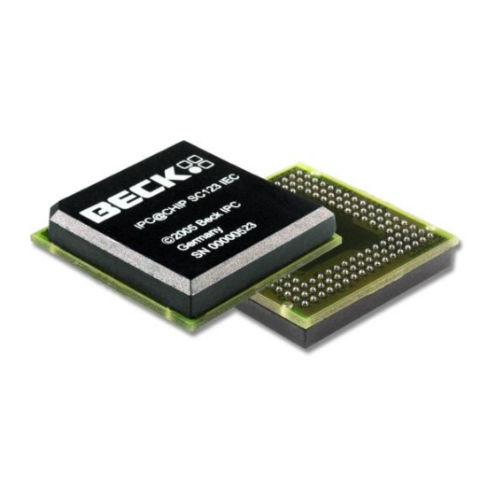
IPC@CHIP SC123/SC143 Hardware Manual V1.06 [18.02.2010] 10.2 Cover Description IPC@CHIP SC123 © 2005 Beck IPC Germany LF IEC HXX SN:000SSSSS Figure 10-2: Cover Cover print variations: Configuration IPC@CHIP SC123 2 MByte Flash Memory IPC@CHIP SC143 8 MByte Flash Memory The suffix LF designates a lead free (RoHS compliant) type of IPC@CHIP. For lead free soldering see chapter 13: Reflow Profile. -
Page 54: Application Examples
Don’t load CPUCLK with any capacity or circuit input. Short raise and fall times of the CPUCLK signal are important for correct working of the internal SDRAM. See chapter 12. The value of R3 depends on EMC requirements, 120 is a suggestion. A crystal with 25MHz ±100ppm is recommended ©2000-2008 BECK IPC GmbH Page 54... -
Page 55: Ethernet Example Circuit
FS23 AGND 49.9 49.9 AGND RJ45 SC1x3 49.9 49.9 75.0 75.0 75.0 75.0 0.022uF 0.1uF 1000pF/2KV Shield AGND Figure 11-2: Ethernet Example Circuit 1 Figure 11-3: Alternative Ethernet Example Circuit 2 from product EB60 ©2000-2008 BECK IPC GmbH Page 55... -
Page 56: External Memory
UCSOUT# WRL/A0 WRH/BHE D[0..15] Figure 11-4: Example circuit for connecting an external memory The pull-down resistor R1 enables A0 at WRL# and BHE# at WRH# after power up of the SC1x3 (see chapter 5.2). ©2000-2008 BECK IPC GmbH Page 56... -
Page 57: Traffic/Link/Speed Leds
Half Duplex Traffic green Full Duplex Traffic LED3 Duplex Figure 11-5: Circuit Example for two bi-coloured LEDs 3.3V LED3 Full Duplex LED2 Activity LED1 Link LED0 100MBit Link Figure 11-6: Circuit Example for four mono-coloured LEDs ©2000-2008 BECK IPC GmbH Page 57... -
Page 58: Sc1X3 Socket
IPC@CHIP SC123/SC143 Hardware Manual V1.06 [18.02.2010] 11.5 SC1x3 Socket There are some BGA test sockets available for SC1x3 prototyping. Beck IPC uses sockets from “Advanced Interconnections”. Type: Flip-Top BGA Socket Ordering Number: 2FRG177-690GGCS Figure 11-7: SC1x3-Socket 11.6 Custom series programming of SC1x3 The program chiptool.exe can be used to program images to the SC1x3. -
Page 59: Cpuclk Handling
The Layout of a PCB can have influences to CPUCLK. Route CPUCLK as short as possible. ©2000-2008 BECK IPC GmbH Page 59... -
Page 60: Reflow Profile
3. PB-free devices cannot be solderd in a leaded process at lower temperatures due to the PB-free material of the BGA balls. Devices with SnPb balls cannot be soldered in a Pb-free process at higher temperatures. Figure 13-1: Reflow Profile ©2000-2008 BECK IPC GmbH Page 60... -
Page 61: History
GmbH. The information in this document is subject to change Right to make changes — BECK IPC GmbH reserves the right without notice. Devices sold by BECK IPC GmbH. Are covered to make changes, without notice, in the products, including...
Need help?
Do you have a question about the IPC SC123 and is the answer not in the manual?
Questions and answers