
Related Manuals for Texas Instruments M-LVDS


Summary of Contents for Texas Instruments M-LVDS
- Page 1 Multipoint-Low Voltage Differential Signaling (M-LVDS) Evaluation Module User’s Guide High Performance Analog April 2004 SLLU039B...
- Page 2 Texas Instruments Incorporated and its subsidiaries (TI) reserve the right to make corrections, modifications, enhancements, improvements, and other changes to its products and services at any time and to discontinue any product or service without notice. Customers should obtain the latest relevant information before placing orders and should verify that such information is current and complete.
- Page 3 Texas Instruments (TI) provides the enclosed product(s) under the following conditions: This evaluation kit being sold by TI is intended for use for ENGINEERING DEVELOPMENT OR EVALUATION PURPOSES ONLY and is not considered by TI to be fit for commercial use. As such, the goods being provided may not be complete in terms of required design-, marketing-, and/or manufacturing-related protective considerations, including product safety measures typically found in the end product incorporating the goods.
- Page 4 EVM WARNINGS AND RESTRICTIONS It is important to operate this EVM within the supply voltage range of 3 V to 3.6 V. Exceeding the specified supply range may cause unexpected operation and/or irreversible damage to the EVM. If there are questions concerning the supply range, please contact a TI field representative prior to connecting the input power.
- Page 5 How to Use This Manual This document contains the following chapters: Chapter 1—The M-LVDS Evaluation Module Chapter 2—Test Setup Chapter 3—Bill of Materials, Board Layout, and PCB Construction Appendix A—Schematic Related Documentation From Texas Instruments and Others Introduction to M-LVDS (SLLA108) LVDS Designer’s Notes (SLLA014A).
-
Page 7: Table Of Contents
The M-LVDS Evaluation Module Overview .............. - Page 8 2−1 EVM Configuration Options 3−1 M-LVDS EVM Bill of Materials 3−2 EVM Layer Stack Up ............
-
Page 9: The M-Lvds Evaluation Module
The M-LVDS Evaluation Module This document describes the multipoint low-voltage differential-signaling (M-LVDS) evaluation module (EVM) used to aid designers in development and analysis of this new signaling technology. The Texas Instruments SN65MLVD200A, SN65MLVD201, SN65MLVD204A, SN65MLVD205A, SN65MLVD206, SN65MLVD207 series are low-voltage differential line drivers and receivers complying with the M-LVDS standard (TIA/EIA−899). -
Page 10: M−Lvds Devices Supported By The Evm
M-LVDS devices are not precluded from being used in a point-to-point or multidrop configuration. In these configurations there can be a distinct advantage to the additional current drive provided by an M-LVDS driver. The M-LVDS devices shown in Table 1−1 all include output slew-rate limited drivers, thus the need for different nominal signaling rates. -
Page 11: M-Lvds Standard Tia/Eia−899
1.2 M-LVDS Standard TIA/EIA−899 The M-LVDS standard was created in response to a demand from the data communications community for a general-purpose high-speed balanced interface standard for multipoint applications. The TIA/EIA−644 standard defines the LVDS electrical-layer characteristics used for transmitting information in point-to-point and multidrop architectures. -
Page 12: Expanded Graph Of Receiver Differential Input Voltage Showing Transition Region
Î Î Î Î Î Î Î Î Î Î Î Î Î Î Î Î Î Î Î Î Î Î −0.05 −2.4 1.3 M-LVDS EVM Kit Contents The M-LVDS EVM kit contains the following: M-LVDS EVM PWB with SN65MLVD201D and SN65MLVD207D installed (6424409B) Additional SN65MLVD203, SN65MLVD206 M-LVDS EVM kit documentation (user’s guide) -
Page 13: Point-To-Point
The point-to-point simplex configuration is shown in Figure 1−3. The setup schematic for this option is shown in Figure 2−1. Although this is not the intended mode of operation for M-LVDS, it works well for high noise or long higher-loss transmission lines. Due to the increased drive current, a single 100-Ω... -
Page 14: Multipoint
Figure 1−6 shows a representation of a five-node multipoint configuration using transceivers. Increased drive current, in addition to the wider common- mode input, allows M-LVDS parts to drive multiple receivers over longer line lengths with up to 2 V of ground noise. -
Page 15: Evm Operation With Separate Power Supplies
Adjust PS1 and PS3 to the supply voltage (3.3 V) and current limit to 50 mA. Set PS2 to 0 V Induce a ground offset by varying the output of PS2. PS2 Output The PS2 output should not exceed ± 2 V to remain within the device ratings. The M-LVDS Evaluation Module Configurations... -
Page 16: Evm Configuration For Including A Ground Potential Difference Voltage Between Nodes
A function or pattern generator capable of supplying 3.3-V signals at the desired signaling rate. A multiple-channel high-bandwidth oscilloscope, preferably above the 1-GHz range Differential or single ended oscilloscope probes. Jumpers removed from W7, W8, W9, W10 The M-LVDS Evaluation Module... -
Page 17: Test Setup
This chapter describes how to setup and use the M-LVDS EVM. Topic Typical Cable Test Configurations Test Results .......... -
Page 18: Typical Cable Test Configurations
Typical Cable Test Configurations 2.1 Typical Cable Test Configurations Each of the following test configurations is a transmission line consisting of a twisted-pair cable connected on the 2-pin connectors (P1, P2, or P3). Table 2−1 shows the possible configurations. In addition to the different transmission topologies, the EVM can also be configured to run off two or three separate power supplies, as described in the previous section. -
Page 19: Point-To-Point Parallel Terminated Simplex Transmission
2.1.2 Point-to-Point Parallel Terminated Simplex Transmission 1) Connect a twisted-pair cable from P1 to P2. 2) Verify resistor R4 and R7 are installed. 3) Remove resistors R5 and R6. This properly terminates the transmission line at both ends. 4) Enable the driver by connecting the jumper on W2 between pin 1 and pin 2, or U1 pin 4 to V 5) Enable the receiver by connecting the jumper on W1 between pin 2 and pin 3, or U1 pin 3 to GND. -
Page 20: Two-Node Multipoint Transmission
Typical Cable Test Configurations Figure 2−3. Two-Node Multipoint Transmission 50-Ω Cable Signal Source with 50-Ω Output 50-Ω Cable Ω cable or Active Voltage Probe into one Channel of Scope Terminated in High Impedance Active Voltage Probe 50-Ω Cable Ω cable or Active Voltage Probe into one Channel of Scope... -
Page 21: Test Results
2.2 Test Results The test configurations described in Section 2.1 were used to simulate point- to-point simplex, parallel-terminated point-to-point simplex, and two-node multipoint. The test results are shown in the following figures. A Tektronix HFS9003 was used to generate input signals, and a Tektronix TDS784D was used to collect the output data. -
Page 22: Parallel Terminated Point-To-Point Parallel Simplex Typical Eye Pattern Data
TP1, R2 is shorted. Type-2 behavior is again observed on the SN65MLVD207 receiver output. Trace three shows the differential voltage on the bus. Note that the bus volt- ages are nominal M-LVDS levels of 1.1 V current driver. Figure 2−5. Parallel Terminated Point-to-Point Parallel Simplex Typical Eye Pattern Data Figure 2−6 represents the two-node multipoint transmission eye patterns... -
Page 23: Bill Of Materials, Board Layout, And Pcb Construction
Bill of Materials, Board Layout, and PCB This chapter contains the bill of materials, board layout of the M-LVDS, and describes the printed-circuit board. Topic Bill of Materials .......... -
Page 24: Bill Of Materials
Bill of Materials 3.1 Bill of Materials Table 3−1. M-LVDS EVM Bill of Materials Item Reference Qty. Designation C1, C2 Capacitor, SMT1206, 50 V, 10%, 0.01 µF C5, C6, C9, Capacitor, SMT1206, 16 V, 10%, 1 µF C3, C4, C7, C8 Capacitor, SMT1210, 10 V, 10%, 10 µF... -
Page 25: Board Layout
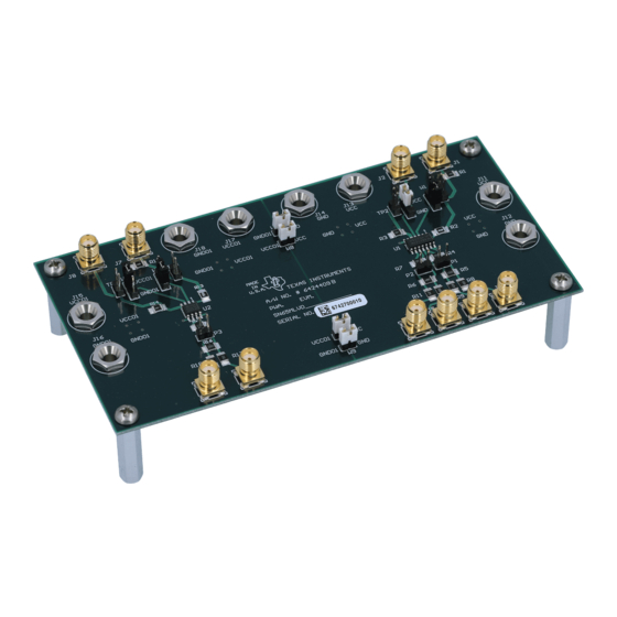
3.2 Board Layout Figure 3−1. Assembly Drawing GND01 W4 W3 VCC01 GND01 VCC01 GND01 The top layer of the EVM contains the controlled impedance and matched length traces. Figure 3−2. Top Layer VCC01 GND01 VCC01 MADE U.S.A. TEXAS INSTRUMENTS A/W NO. # 6424409B PWA. - Page 26 Board Layout The second layer of the EVM has the separate ground planes. These are the reference planes for the controlled impedance traces on the top layer. Figure 3−3. Second Layer Ï Ï Ï Ï Ï Ï Ï Ï Ï Ï Ï Ï Ï Ï Ï Ï...
- Page 27 The bottom layer of the EVM contains bulk and decoupling capacitors to be placed close to the power and ground pins on the device. Figure 3−5. Bottom Layer VCC01 GND01 Bill of Materials, Board Layout, and PCB Construction Board Layout...
-
Page 28: Pcb Construction
PCB Construction 3.3 PCB Construction Information in this section was obtained from the following source: Electromagnetic Compatibility Printed Circuit Board and Electronic Module Design, VEC workshop, Violette Engineering Corporation. Characteristic impedance is the ratio of voltage to current in a transmission line wave traveling in one direction. - Page 29 Figure 3−6. Trace Configurations in Printed-Circuit Boards Board Material MICROSTRIP Stripline construction is the preferred configuration for differential signaling. This configuration reduces radiated emissions from circuit board traces due to better control of the lines of flux. The additional ground plane also allows for better control of impedance on the traces.
-
Page 30: Evm Layer Stack Up
PCB Construction Table 3−2 shows the layer stack up of the EVM with the defined trace widths for the controlled impedance etch runs using microstrip construction. Table 3−2. EVM Layer Stack Up Material Layer Layer Thickness Type: Type (mils) FR 406 Signal 0.0006 PREPREG... -
Page 31: A Schematic
Appendix A Schematic This Appendix contains the EVM schematic. Schematic... - Page 32 Recei ver O ut put 49. 9 Recei ver Enabl e D r i ver Enabl e D r i ver I nput 49. 9 G N D V CC01 Recei ver O ut put R12* 49. 9 Recei ver Enabl e D r i ver Enabl e D r i ver I nput 49.
Need help?
Do you have a question about the M-LVDS and is the answer not in the manual?
Questions and answers