Advertisement
Quick Links
SERVICE MANUAL
HOME CINEMA DVD/CD CONTROL CENTER
HOME CINEMA
DVD-AUDIO/VIDEO CONTROL CENTER
STANDBY/ON
STB
VCR
TV
AUDIO
TV
TAPE
CDR
FM/AM
TV DIRECT
STB
VCR
DVD
/FF
TV/VIDEO
REW/
TUNING/GROUP
REPEAT
SLEEP
FM MODE
STROBE
TV/STB CH
EFFECT
CENTER
CONTROL
1
2
3
ANALOG
TEST
REARáL
/DIGITAL
4
5
6
INPUT
AUDIO
SURR ON/OFF
REARáR
7
8
9
STANDBY
STANDBY/ON
SUBTITLE
SURR MODE
Ð SUBWOOFER +
10/0
+10
VFP
100+
TV RETURN
PROGRESSIVE
DIMMER
ANGLE
+
+
PAGE
TV VOL
VOLUME
MUTING
ZOOM
Ð
Ð
TA/NEWS/INFO
DIGEST
TOP MENU
MENU
PTY
PTY SEARCH
PTY
CHOICE
ENTER
ON SCREEN
RETURN
DISPLAY
REMOTE CONTROL RM-SRXDV5R
Contents
Safety precautions --------------------------------------------------------
Preventing static electricity ----------------------------------------------
Disassembly method ------------------------------------------------------
Adjustment method -------------------------------------------------------
Description of major ICs -------------------------------------------------
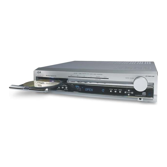
RX-DV5RSL
RX-DV5R HOME CINEMA DVD-AUDIO/VIDEO CONTROL CENTER
DVD
STB
VCR
INPUT
SURROUND
DVD AUDIO
ANALOG/DIGITAL
ON/OFF
MODE
INPUT ATT.
REC MODE
COPYRIGHT
2002 VICTOR COMPANY OF JAPAN, LTD.
B ----------------------- U.K.
E --- Continental Europe
EN----- Northern Europe
TV
TAPE/CDR
FM/AM
TV DIRECT
MASTER VOLUME
SOURCE NAME
SETTING
ADJUST
MEMORY
CONTROL
DVD/SUPER VCD/VCD/CD
RX-DV5RSL
Area suffix
COMPACT
SUPER VIDEO
1-2
1-4
1-5
1-14
1-16~52
No.21186
Oct. 2002
Advertisement

Related Manuals for JVC RX-DV5RSL


Summary of Contents for JVC RX-DV5RSL
- Page 1 RX-DV5RSL SERVICE MANUAL HOME CINEMA DVD/CD CONTROL CENTER RX-DV5RSL Area suffix B ----------------------- U.K. E --- Continental Europe EN----- Northern Europe HOME CINEMA DVD-AUDIO/VIDEO CONTROL CENTER STANDBY/ON AUDIO TAPE FM/AM TV DIRECT TV/VIDEO REW/ TUNING/GROUP REPEAT SLEEP FM MODE STROBE...
- Page 2 RX-DV5RSL 1. This design of this product contains special hardware and many circuits and components specially for safety purposes. For continued protection, no changes should be made to the original design unless authorized in writing by the manufacturer. Replacement parts must be identical to those used in the original circuits. Services should be performed by qualified personnel only.
- Page 3 RX-DV5RSL (U.K only) 1. This design of this product contains special hardware and many circuits and components specially for safety purposes. For continued protection, no changes should be made to the original design unless authorized in writing by the manufacturer.
- Page 4 RX-DV5RSL Preventing static electricity 1. Grounding to prevent damage by static electricity Electrostatic discharge (ESD), which occurs when static electricity stored in the body, fabric, etc. is discharged, can destroy the laser diode in the traverse unit (optical pickup). Take care to prevent this when performing repairs.
- Page 5 RX-DV5RSL Disassembly method Top cover Removing the top cover (See Fig.1) Remove the four screws marked A attaching the top cover on both sides of the body. Remove the three screws marked B on the back of the body. Fig.1 Remove the top cover from behind in the direction of the arrow while pulling both sides outward.
- Page 6 RX-DV5RSL Removing each board connected to the main board (See Fig.6 to 10) Prior to performing the following procedures, remove the top cover and rear panel. CN201 Cut off the tie band fixing the harness. CN212 Disconnect the video board from the connector CN612 CN911 CN912 on the main board.
- Page 7 RX-DV5RSL Removing the amplifier board (See Fig.11, 12) band Prior to performing the following procedures, remove the top cover, and rear panel. CN201 CN212 Disconnect the wire from the connector CN201 on the amplifier board. board Disconnect the amplifier board from the connector CN212 on the main board.
- Page 8 RX-DV5RSL Removing the DVD / CD unit (See Fig.15) Prior to performing the following procedures, remove the top cover, rear cover and DSP board. / CD unit Pull up the two plastic rivet attaching the DVD / CD unit dust proof cover.
- Page 9 RX-DV5RSL Removing the power transformer (See Fig.18, 19) Prior to performing the following procedures, remove CN121 Power the top cover and rear panel. supply CN111 board If necessary, cut off the tie band fixing the harness. Solder points Disconnect the harness from the connector CN101 on the power / fuse board.
- Page 10 RX-DV5RSL Removing the tuner board (See Fig.21) Main Prior to performing the following procedures, remove board the top cover, rear panel, video board, DSP board and video select board. Disconnect the card wire from the connector CN301 Tuner on the main board.
- Page 11 RX-DV5RSL <DVD / CD unit> Prior to performing the following procedures, remove DVD / CD tray the DVD / CD unit. Removing the DVD / CD tray (See Fig.1, 2) Loading cam lever Push the cam lever toward the center side of the DVD / CD unit in the direction of the arrow and draw Fig.1...
- Page 12 RX-DV5RSL Removing the the top cover DVD / CD unit Top cover (See Fig.4) Stopper Prior to performing the following procedures, remove the DVD / CD tray. Remove the four screws marked A attaching the top cover on the DVD / CD unit.
- Page 13 RX-DV5RSL Removing the DVD / CD mechanism DVD / CD unit holder assembly (mechanism included) Top cover (See Fig. 7, 8) Prior to performing the following procedures, remove the DVD / CD tray, the DVD / CD servo board and top cover.
- Page 14 RX-DV5RSL Adjustment method Measurement instruments required for adjustment Radio input signal 1. Low frequency oscillator, AM modulation frequency : 400Hz This oscillator should have a capacity to output 0dBs Modulation factor : 30% to 600ohm at an oscillation frequency of 50Hz-20kHz.
- Page 15 RX-DV5RSL Initialization method of DVD section When microprocessor ICs or pick-up has been replaces, initialize the DVD player in the following manner. If tray is not completely close up, make power to standby from on to close up the tray.
- Page 16 RX-DV5RSL Description of major ICs AK4527BVQP (IC601) : A/D,D/A converter 1. Pin layout Top View 2. Pin function (1/2) Symbol Function SDOS SDTO Source Select Pin (Note 1) "L" : Internal ADC output, "H" : DAUX input OSKS Control Mode Select Pin "L"...
- Page 17 RX-DV5RSL Pin function (2/2) AK4527 Symbol Function Connect to GND ICKS No internal bonding. Analog Input Format Select Pin, Digital Power Supply ADIF "H" : Full-differential input, "L" : Single-ended input Chip Address 1 Pin, Connect to GND CAD1 Chip Address 0 Pin, Connect to GND...
- Page 18 RX-DV5RSL MN101C35DKF (IC701) : Panel MICOM 1. Pin layout 2. Pin function Symbol Function Pin No. TXD/SBO0/P00 No connect RXO/SBI0/P01 No connect SBT0/P02 No connect SBO1/P03 No connect SBI1/P04 No connect SBT1/P05 No connect BUZZER/P06 No connect Power supply OSC2...
- Page 19 RX-DV5RSL MN101C35DKF Pin No Symbol Function No connect No connect No connect No connect DGT17/P67 DGT16/P66 No connect No connect DGT15/P65 DGT14/P64 No connect DGT13/P63 GRID1 DGT12/P62 GRID2 DGT11/P61 GRID3 DGT10/P60 GRID4 DGT9/P41 GRID5 DGT8/P40 GRID6 SEG0/DGT7/P77 GRID7 GRID8 SEG1/DGT6/P76...
- Page 20 RX-DV5RSL MN101C49GKG (IC761) : System MICOM 1. Pin layout 2. Pin function Pin No. Symbol Function VREF Connect to GND NTSTEL(RGBESL) VCR S/C SW DBS S/C SW SAFETY SHORT&TH DET (A/D) OUTLEVEL DETECT (A/D) VCR IN (A/D) STB IN (A/D)
- Page 21 RX-DV5RSL MN101C49GKG Pin No. Symbol Function SBT1 DSP CLK CBO3 VOL DATA SBI3 VOL LATCH SBT3 VOL CLK D.O.MUTE INT/PROG INT/PROG KEY0 HEADPHONE RELAY KEY1 EEDO KEY2 EEDI KEY3 EECK KEY4 EECS KEY5 FRONT SPK RELAY KEY6 CENTER SPK RELAY...
- Page 22 RX-DV5RSL UPD784215AGC (IC681) : Dital signal controller 1. Pin layout 2. Pin function (1/2) Pin No. Symbol Function Non connect Power supply terminal Connecting the crystal oscillator for system main clock Connecting the crystal oscillator for system main clock Connect to GND...
- Page 23 RX-DV5RSL Pin function (2/2) UPD784215AGC167 Pin No. Symbol Function Interface I/O terminal with microcomputer MILP Interface I/O terminal with microcomputer MIACK Non connect Non connect Reset signal output of DSP DSPRST Non connect 54~63 Interface I/O terminal with microcomputer CODEC OUT...
- Page 24 RX-DV5RSL AN8703FH-V (IC101) : Front-end processor for DVD 1.Pin layout 48~33 49~64 32~17 1~16 2. Block diagram 46 48 47 31 30 HOLD VIN5 FBAL Level VIN6 Cont. VIN7 Det. VIN8 Vol. Adj. Level Cont. OFLR Det. OFTR Boost Cont.
- Page 25 RX-DV5RSL 3.Pin function (2/2) Pin No. Symbol Function POFLT Tracking detection threshold level DTRD Data slice data read signal input (for RAM) IDGT Data slice address gate signal input (for RAM) STANBY Standby mode control SEN (serial data input) SCK (serial data input)
- Page 26 RX-DV5RSL M61516FP (IC301) : Sound controller 1. Block diagram TRE R DVDD OUTPUT GAIN BASS R2 TINT CONTROL OUTPUT GAIN ZERO CROSS CONTROL DETECTOR & BASS R1 VOLGND2 TIMER DETECTOR TONE OUTPUT SELECTOR FRIN2 FLVIN FL VOL SRIN2 TNEOUT FL VOL...
- Page 27 RX-DV5RSL 2.Pin function Pin No. Symbol Function 74,75,76,77,78, INLA,B,C,D,E,F,G,H,I,J Lch input 79,80,1,2,3 4,5,6,7,59,60,61 REC L1,L2,L3,L4 REC output /REC R1,R2,R3,R4 8,22,52,53 VOLGND1,2,3,4 Analog GND for vol. 9,51 FLIN1/FLIN2 FLch input 10,50 SLIN1/SLIN2 SLch input 11,49 SBLIN1/SBLIN2 SBLch input 12,48 CIN1/CIN2 Cch input...
- Page 28 RX-DV5RSL NDV8611VWA (IC501) : Pantera 1.Pin layout 2. Block diagram digital audio 120 - 61 Video I/O Port audio DAC NTSC Audio MPEG Video Audio digital audio Output Video Output Video SCART Decoder Processor Processor Encoder 181 - 240 Serial...
- Page 29 RX-DV5RSL 3.Pin function (2/4) Pin No. Symbol Function SDRAM data bus VDDIO I/O pad power =3.3V 45, 46 SDRAM data bus Core and Ring ground SDRAM data bus VSSIO I/O pad ground 50-52 SDRAM data bus VDDIO I/O pad power =3.3...
- Page 30 RX-DV5RSL 3.Pin function (3/4) Pin No. Symbol Function VDDDAC DAC digital power VSSDAC DAC digital ground DAC3 Video DAC3 output Cascaded DAC differential output used to dump current into external resistor for power DAC2 Video DAC2 output VAA3 DAC analog power...
- Page 31 RX-DV5RSL 3.Pin function (4/4) Pin No. Symbol Function Core and Ring ground 202-203 External input/output VSSIO I/O pad ground 205-209 External input/output VDDIO I/O pad power =3.3V External input/output Core power =1.8V DSYNC DVD parallel mode Sector Sync DRQE DVD parallel mode Data Request...
- Page 32 RX-DV5RSL MN103S26EGA (IC301) : Super optical disc controller 1.Terminal layout 2.Block diagram Host I/F DVD-ROM Analog MPEG I/F Formatter CD-PRE ATAPI High speed IO bus Instruction Servo I/O CGEN memory (core 1 I/O) (40KB) 32 bit CPU core 2Mbit Servo core...
- Page 33 RX-DV5RSL 3.Pin function (MN103S26EGA : 2/4) Symbol Description Pin No. Read signal input from system controller System control data 37~44 CPUDT7~0 Non connect CLKOUT1 Test mode switch signal MMOD System reset NRST Master terminal polarity switch input MSTPOL Non connect...
- Page 34 RX-DV5RSL 3.Pin function (MN103S26EGA : 3/4) Symbol Description Pin No. PLFLT1 Connect to capacitor 1 for PLL AVSS Connect to ground for analog circuit Connect to resistor for VREF reference current source VREFH Reference voltage input (2.2V) PLPG Non connect VHALF Reference voltage input (1.65V)
- Page 35 RX-DV5RSL 3.Pin function (MN103S26EGA : 4/4) Symbol Description Pin No. Connect to ground VDD3 Power supply terminal for I/O (3.3V) HDD1 ATAPI host data 1 HDD13 ATAPI host data 13 HDD2 ATAPI host data 2 HDD12 ATAPI host data 12...
- Page 36 RX-DV5RSL W986432DH-7 (IC505) : 32 Bits SDRAM 1.Pin layout 2.Pin function Symbol Function Pin No. Power for input buffers and logic circuit inside DRAM. (+3.3V) Multiplexed pins for data out put and input. Separated power from VCC, to improve DQ noise immunity. (+3.3V) VccQ Multiplexed pins for data out put and input.
- Page 37 RX-DV5RSL W986432DH-7 Symbol Function Pin No. Multiplexed pins for data out put and input. 36~37 DQ19~20 Separated power from VSS, to improve DQ noise immunity. VssQ Multiplexed pins for data out put and input. 39~40 DQ21~22 Separated power from VCC, to improve DQ noise immunity. (+3.3V) VccQ Multiplexed pins for data out put and input.
- Page 38 RX-DV5RSL 3. Block diagram Clock buffer Control signal generator Command buffer Column decoder Column decoder Cell array Cell array bank #0 bank #1 Mode Sense amplifier Sense amplifier register Address buffer Data control buffer circuit DQ31 DQM0~3 Column Refresh counter...
- Page 39 RX-DV5RSL TC9446F-025 (IC631) : Digital signal processor for dolby digital (AC-3) / DTS audio decode Pin No. Symbol Function Reset signal input terminal (L:reset H: normal operation) Microcomputer interface mode selection input terminal (L:serial H:IC bus) MIMD Microcomputer interface chip select input terminal...
- Page 40 RX-DV5RSL MN102L62GLF (IC401) : Unit CPU Pin function Symbol Function Symbol Function Pin No. Pin No. Micon wait signal input Non connect WAIT SWUPDN Read enable Connect to ground MECHA_H/V Spindle muting output to IC251 Mechanism state signal input SPMUTE...
- Page 41 RX-DV5RSL TC74HCU04AF (IC621) : Inverter TC7SET32FU (IC683) : Z-Input or gate 1. Pin layout 2. Truth table 1. Block diagram IN B IN A OUT Y TC74HCU08AF (IC612) : Inverter 1. Block diagram 2.Truth table TC74HC4072AF (IC611) : 4-Input gate 1.
- Page 42 RX-DV5RSL LP61L1024S-12-X (IC641) : SRAM 1. Pin layout 2. Block diagram DECODER CORE ARRAY I/O1 CONTROL DATA I/O I/O8 I/O8 I/O7 I/O1 I/O6 I/O2 3. Pin function I/O5 I/O3 I/O4 Symbol Description A0 - A16 Address Input I/O1 - I/O8...
- Page 43 RX-DV5RSL AK93C65AF-X (IC510) : EEPROM 1.Pin layout 8 PIN SOP 2.Block diagram DATA REGISTER R/W AMPS AUTO ERASE EEPROM INSTRUCTION REGISTER INSTRUCTION DECODE, CONTROL 4096bit 256 x 16 CLOCK ADD. DECODER GENERATION BUFFERS VPP SW VREF GENERATOR 3.Pin function Pin no.
- Page 44 RX-DV5RSL BA6664FM (IC251) : Motor driver 1. Block diagram DRIVER GAIN SWITCH GAIN CONTROL CURRENT SENSE AMP HALL AMP TORQUE SENSE AMP SHORT BRAKE BRAKE MODE Hall Bias 2.Pin function Pin No. Symbol Function Pin No. Symbol Function N3Phase synthesized FG signal...
- Page 45 RX-DV5RSL SAA6588 (IC302) : RDS detector 2.Pin function 1.Pin layout Symbol Function Multi-path rectifier output Non connect Test control input pin SCOUT Oscillator output OSCO OSCO Vref Oscillator input OSCI OSCI Digital ground (0V) VSSD Digital power supply (5V) VDDD...
- Page 46 RX-DV5RSL SST39VF160 (IC508, IC509) : EEPROM 1. Pin layout DQ15 DQ14 DQ13 DQ12 DQ11 DQ10 2. Block diagram EEPROM X-Decoder Cell Array Memory Address Address Buffer & Latches Y-Decoder Control Logic I/O Buffers & Data Latches DQ15~DQ0 3. Pin function...
- Page 47 RX-DV5RSL 74LCX32MTC-X (IC522) : OR gate 1.Block diagram 2.Pin function Symbol Description An,Bn Inputs Outputs 74LCX373MTC-X (IC512, IC513) : Latch 1.Pin layout 2. Pin function 3.Truth table Symbol Description Inputs Outputs D0-D7 Data Inputs Latch Enable Input Output Enable Input...
- Page 48 RX-DV5RSL BA5983FM (IC201) : 4ch driver 1.Block diagram STAND BY Level Shift Level Shift Level Shift Level Shift STAND BY CH1/2/3 2.Pin function Function Symbol Symbol Function Pin No. Pin No. Input for Bias-amplifier VO4(+) Non inverted output of CH4...
- Page 49 RX-DV5RSL K4S643232E-TC60 / K4S643232E-TC70 (IC505) : SDRAM 1.Pin layout 2. Block diagram DQ15 VDDQ VSSQ DQ14 DQ13 Data Input Register VSSQ VDDQ DQ12 LDQM DQ11 VDDQ VSSQ Bank Select DQ10 VSSQ VDDQ 512K DQM0 DQM1 512K 512K 512K A10/AP Column Decoder...
- Page 50 RX-DV5RSL LA73054 (IC401) : Video driver 1. Block diagram CLAMP 2Step Amp1 C_OFFSET DC_CLT DRIVER 2Step LPF1 DRIVER Amp2 2Step LPF1 CLAMP Amp3 DRIVER SYNC PEDESTAL CLAMP LPF2 2Step Amp4 DRIVER CLAMP LPF1 LPF2 2Step PEDESTAL CLAMP Amp5 DRIVER LPF1...
- Page 51 RX-DV5RSL SI-8033JF (IC191) / SI-8050JF (IC192) / SI-8090JF (IC193) : Switching regulator 1. Block diagram SW OUT Over-current PReg protection ON/OFF ON/OFF Latch Reset Soft- & Start Driver Oscillator Heating protection Comparator Error amp Standard voltage MM1563DF-X (IC615) : Regulator 1.
- Page 52 RX-DV5RSL MN35505 (IC901, IC931, IC961) : DAC 1. Pin layout 2. Pin function Symbol Function Pin No. Control signal for DAC Digital data input LRCK L and R clock for DAC Bit clock for DAC Control signal for DAC Power supply...
- Page 53 RX-DV5RSL < M E M O > 1-53...
- Page 54 RX-DV5RSL VICTOR COMPANY OF JAPAN, LIMITED AUDIO & COMMUNICATION BUSINESS DIVISION PERSONAL & MOBILE NETWORK BUSINESS UNIT. 10-1,1chome,Ohwatari-machi,Maebashi-city,371-8543,Japan Printed in Japan (No.21186) 200210...
- Page 55 RX-DV5RSL SCHEMATIC DIAGRAMS HOME CINEMA DVD/CD CONTROL CENTER RX-DV5RSL Area suffix CD-ROM No.SML200210 B ----------------------- U.K. E --- Continental Europe EN----- Northern Europe HOME CINEMA DVD-AUDIO/VIDEO CONTROL CENTER STANDBY/ON AUDIO TAPE FM/AM TV DIRECT TV/VIDEO REW/ TUNING/GROUP REPEAT SLEEP FM MODE...
- Page 56 RX-DV5RSL In regard with component parts appearing on the silk-screen printed side (parts side) of the PWB diagrams, the parts that are printed over with black such as the resistor ( diode ( ) and ICP ( ) or identified by the " " mark nearby are critical for safety.
- Page 57 RX-DV5RSL Block diagram LVA10334 SDRAM COAXIAL SDTO, SDTI1-3 IC641 AD/DA IC621 CONVERTER AMP. IC601 IC602,603 PANEL MICOM SELECTOR IC702 OPTICAL IC611 MICOM IC701 IC631 AMP. IC612 IC681 REMOCON IC651,652, 661,671,672 OPTICAL DSP CLK, DSP STATUS, DSP READY, DSP RESET FL DISPLAY...
- Page 58 RX-DV5RSL RX-DV5RSL Standard schematic diagrams Power supply section QQT0371-004 T101 Sheet 2/11 CN101 QGA7901C1-02 CN111 CN115 QGF1205C1-10 QGA3901C1-05 Power board POWER PW151 PW101 S1RELAY QUB112-30PPPP F101 QUB112-30PPPP PW102 T2.0AL TA101 PW152 F102 QUB111-32PPPP Sheet 2/11 QUB111-32PPPP QNZ0079-001Z T100mAL PW103 PW153...
- Page 59 RX-DV5RSL Main section Sheet 9/11 Sheet 9/11 Main board QGA2501C3-02Z HPSW CN513 CN512 CN122 QGB2027M9-26 QGB2027M9-26 HPRELAY Q162 Q161 Q151 C158 Q171 R161 R151 R181 Q181 R184 R141 R145 Q145 R162 R169 R171 R154 Q141 D291 KTA1046/Y 2SD2395/EF KTC3203/OY 2SD2395/EF...
- Page 60 RX-DV5RSL RX-DV5RSL Amp. & Speaker terminal section Amp. board IC201 IC202 JCV8007 JCV8008 C1223 R2231 C223 C224 C1224 C2223 Q2231 R227 KTC3200/GL R2227 100p 100p 100p 100p 100p R228 R1228 R1232 R1227 Q1232 KTC3200/GL R221 R1231 R1221 Q1231 KTC3200/GL RY263...
- Page 61 RX-DV5RSL FL display & System control section FL board C713 C714 4.7/50 4.7/50 C715 4.7/50 DI701 DI701 QLF0101-001 QLF0101-001 Q701 KRC107S-X Q700 KRC107S-X M_CLK CN701 M_COMMAND QGF1205F1-13 M_STATUS M_CLK R1701 M_COMMAND R1702 R752 R753 M_STATUS R1703 IC701 JOG2 M_CS R1704...
- Page 62 RX-DV5RSL RX-DV5RSL DSP section C624 D621 TP621 K601 MA111 R622 J601 NQR0269-004X QNN0481-001 C622 1/50 TP624 TP622 C629 R623 100P 4.7k D622 R624 C623 MA111 C619 0.01 R619 R620 (SDTI1-3) C620 100/16 R2515 TP509 TP623 R651 C2507 LIN+ UN661 TP501...
- Page 63 RX-DV5RSL Video signal output section Scart jack board (TV_RED_OUT) (TV_RED_OUT) (VCR_R/C) (DVD_R/C) R324 VCR_ROUT C1493 R323 J402 VCR_LOUT QNZ0516-001 VCR_B C328 C326 C325 C327 330p 330p 330p 330p (VCR_R/C) R306 VCR_R (DVD_R/C) C304 330p CN401 C303 R305 QGF1205F1-17 330p VCR_L...
- Page 64 RX-DV5RSL RX-DV5RSL DVD System control section S3.3V D3.3V D1.8V (STD0-7) K301 K302 K303 K304 R341 5.6K (T1CD,T2CD,TA,TB,TC,TD) C144 0.01/16 (STD0-7) C145 CN101 QGF0522F1-30W DGND Sheet 8/11 T2CD HDTYPE ODCIRQ2 F2CD R318 ODCIRQ R319 T1CD C347 C141 TP309 0.1/16 0.1/16 TP308 C115 0.1/16...
- Page 65 RX-DV5RSL DVD Servo section D3.3V R998 R995 D1.8V D3.3V Sheet 9/11 K504 NQR0007-002X R505 R506 Sheet 7/11 (STD0-7) R507 C527 C524 47/4 47/4 D3.3V R508 K501 NQR0007-002X PWE0 IC505 K4S643232E-TC70 C511 C512 0.1/16 47/4 MD10 C501 MD11 0.1/16 R584 C514 0.1/16...
- Page 66 RX-DV5RSL RX-DV5RSL DVD Memory section Sheet 8/11 D3.3V D3.3V S3.3V D3.3V LADD16 CN502 IC509 QGB2027L1-26X C910 SST39VF160-9CEK IC512 LADD15 74LCX373MTC-X C904 0.1/16 R604 LADD14 C906 0.1/16 LADD13 LADD6 LADD19 LADD12 AD15 CN501 AD19 C902 0.1/16 LADD11 LADD10 AD14 AD18 LADD9...
- Page 67 RX-DV5RSL DVD Pin terminal voltage SHEET 10/11 2-11...
- Page 68 RX-DV5RSL RX-DV5RSL DAC section DAC board IC911 IC921 IC991 NJM4580E-W NJM4580E-W NJM4580E-W C951 R915 R923 C917 C925 4.7/25 C919 4.7/25 R953 R955 0.01 R917 R925 3.3k C913 120p C934 0.001 R929 R931 DAC0CS C953 C927 C911 R951 R943 DCLK 4.7/25...
- Page 69 RX-DV5RSL Printed circuit boards Main board HS182 Q770 CN121 CN122 Q182 R395 R392 R391 R386 R385 R166 CN291 CN125 R168 R162 R182 C184 R164 C183 R181 Q181 Q164 CN231 D125 D162 R183 C162 D181 Q183 R393 R388 R382 R381 R387...
- Page 70 RX-DV5RSL RX-DV5RSL Amplifier / power supply board Sub trans. board Power board R123 HS102 R106 Q103 R103 R102 CN115 TA102 TA101 PW102 R104 PW114 FC101 Q102 D109 R122 D107 PW103 C101 C104 D116 D118 R121 D105 R101 CN101 R126 PW101...
- Page 71 RX-DV5RSL Front board H. Sensor board FL board C711 R1291 D706 D705 D708 CN701 S718 S719 S720 S717 R1292 R720 R719 R721 D702 R711 S714 PW701 S716 S715 R710 R709 S712 S713 S711 FW703 FW701 LED board JS701 D710 FW702...
- Page 72 RX-DV5RSL RX-DV5RSL DVD board DSP board Forward side Forward side C690 R676 R2520 R2510 R2508 R2518 R2522 C2508 C2518 L501 R619 R2516 R2512 C907 C638 R644 C2516 R2514 C2514 C619 C620 R641 C2504 TPFG4 R583 R642 C631 R2502 C637 C908...
- Page 73 RX-DV5RSL DAC board Forward side C934 C907 R915 R923 C908 C906 C905 C913 R929 C910 R959 C941 R926 C912 R941 R943 Q901 R933 R918 C927 R944 C901 Q902 IC911 R912 IC901 R934 R942 R960 C900 R930 C928 C942 R1941 R1913...
- Page 74 RX-DV5RSL VICTOR COMPANY OF JAPAN, LIMITED AUDIO & COMMUNICATION BUSINESS DIVISION PERSONAL & MOBILE NETWORK BUSINESS UNIT. 10-1,1chome,Ohwatari-machi,Maebashi-city,371-8543,Japan Printed in Japan No.21186SCH 200210...
- Page 75 RX-DV5RSL PARTS LIST [RX-DV5RSL] * All printed circuit boards and its assemblies are not available as service parts. Area Suffix B ----------------------------------- U.K. E -------------- Continental Europe EN ---------------- Northern Europe - Contents - Exploded view of general assembly and parts list (Block No.M1)
- Page 76 RX-DV5RSL < M E M O >...
- Page 77 RX-DV5RSL Exploded view of general assembly and parts list Block No. DSP board Amp.board Scart board Amp. sub Amp. H.Sensor DAC board Speaker SW.board Main board Power board FL board Control board Sub trans. board H.P. board...
- Page 78 RX-DV5RSL RX-DV5RSL Parts list (General assembly) Parts list (General assembly) Block No. M1MM Block No. M1MM Item Parts number Parts name Q'ty Description Area Item Parts number Parts name Q'ty Description Area LV10652-008A FRONT PANEL QYSBSGG3008Z TAP.SCREW 1 H.P PWB+CH.B...
- Page 79 RX-DV5RSL DVD mechanism assembly and parts list Block No. EXL-V72-1YPC 12.0mm 0.2mm 33 13 65.2mm 0.2mm Grease CFD-4007ZYZ JVG-31N PG-641 1401C...
- Page 80 RX-DV5RSL Parts list (DVD mechanism) Block No. MJMM Item Description Parts number Parts name Q'ty Area LE20520-002A MECHA.BASE LE20516-001A SPINDLE BASE QYSDST2605M SCREW LE30909-001A FEED HOLDER ASS QAR0165-001 FEED MOTOR LV41510-001A FEED GEAR T SCREW QYSPSPU2040M LV41512-001A FEED GEAR E...
- Page 81 RX-DV5RSL DVD loading base assembly and parts list Block No. 21 BACK SIDE FMU-DV5-1M Grease =JVG-31N =JVS-1003 BACK SIDE...
- Page 82 RX-DV5RSL Parts list (DVD loading base) Block No. MNMM Item Description Parts number Parts name Q'ty Area LV10454-007A-CK LOADING BASE QAR0164-001 MOTOR 1 MABUCHI LV42087-001A MOTOR PULLEY QYSPSPU1730Z SCREW 1 FOR MOTOR VKZ4777-003 MINI SCREW LV42209-001A BELT LV42084-002A PULLEYGEAR MIDDLE GEAR...
- Page 83 RX-DV5RSL Electrical parts list (Main board) Block No. 01 Item Remarks Item Remarks Parts number Parts name Area Parts number Parts name Area C 131 QFLC2AJ-104Z M CAPACITOR .10MF 5% 100V C 386 QEKC1HM-106Z E CAPACITOR 10MF 20% 50V C 132...
- Page 84 RX-DV5RSL Electrical parts list (Main board) Block No. 01 Item Remarks Parts number Parts name Area Item Parts number Parts name Remarks Area C1387 QETN1HM-106Z E CAPACITOR 10MF 20% 50V HS182 E70306-001 HEAT SINK C1388 QETN1HM-106Z E CAPACITOR 10MF 20% 50V...
- Page 85 RX-DV5RSL Electrical parts list (Main board) Block No. 01 Item Remarks Item Parts number Parts name Remarks Area Parts number Parts name Area Q 766 KRC105S-X CHIP D.TR. R 351 NRSA63J-474X MG RESISTOR Q 767 KRC105S-X CHIP D.TR. R 352...
- Page 86 RX-DV5RSL Electrical parts list (Main board) Block No. 01 Item Remarks Item Parts number Parts name Remarks Area Parts number Parts name Area R 776 NRSA63J-103X MG RESISTOR R1399 NRSA63J-103X MG RESISTOR R 777 NRSA63J-103X MG RESISTOR R1413 NRSA63J-750X MG RESISTOR...
- Page 87 RX-DV5RSL Electrical parts list (Scart board) Block No. 02 Item Remarks Item Remarks Parts number Parts name Area Parts number Parts name Area C 303 NCS31HJ-331X C CAPACITOR R1407 NRSA63J-750X MG RESISTOR C 304 NCS31HJ-331X C CAPACITOR R1408 NRSA63J-473X MG RESISTOR...
- Page 88 RX-DV5RSL Electrical parts list (Amp. board) Block No. 03 Item Remarks Item Remarks Parts number Parts name Area Parts number Parts name Area C 101 QFLC2AJ-472Z M CAPACITOR 4700PF 5% 100V CN222 WJP0040-001A E-SH C WIRE C-B C 102 QETN1EM-477Z...
- Page 89 RX-DV5RSL Electrical parts list (Amp. board) Block No. 03 Item Remarks Item Remarks Parts number Parts name Area Parts number Parts name Area D 293 1SS119-041-T2 SI DIODE R 222 QRJ146J-101X UNF C RESISTOR 100 5% 1/4W D1221 MTZJ15C-T2 Z DIODE...
- Page 90 RX-DV5RSL Electrical parts list (Amp. board) Block No. 03 Item Parts number Parts name Remarks Area R1229 QRE141J-183Y C RESISTOR 18K 5% 1/4W R1230 QRE141J-183Y C RESISTOR 18K 5% 1/4W R1231 QRE141J-473Y C RESISTOR 47K 5% 1/4W R1232 QRE141J-473Y C RESISTOR...
- Page 91 RX-DV5RSL Electrical parts list (Front board) Block No. 04 Item Remarks Item Remarks Parts number Parts name Area Parts number Parts name Area BK701 LV42882-001A PUSH SWITCH R 705 NRSA63J-102X MG RESISTOR BK702 LV42881-001A PUSH SWITCH R 706 NRSA63J-122X MG RESISTOR...
- Page 92 RX-DV5RSL Electrical parts list (Front board) Block No. 04 Item Remarks Parts number Parts name Area S 714 QSW0683-001Z PUSH SWITCH S 715 QSW0683-001Z PUSH SWITCH S 716 QSW0683-001Z PUSH SWITCH S 717 QSW0683-001Z PUSH SWITCH S 718 QSW0683-001Z PUSH SWITCH...
- Page 93 RX-DV5RSL Electrical parts list (DSP board) Block No. 05 Item Remarks Item Remarks Parts number Parts name Area Parts number Parts name Area C 601 QETN0JM-107Z E CAPACITOR 100MF 20% 6.3V C2507 NCS31HJ-330X C CAPACITOR C 602 NCF31CZ-104X C CAPACITOR...
- Page 94 RX-DV5RSL Electrical parts list (DSP board) Block No. 05 Item Remarks Item Remarks Parts number Parts name Area Parts number Parts name Area IC682 MM1613DN-X R 687 NRSA63J-432X MG RESISTOR IC683 TC7SET32FU-X R 688 NRSA63J-822X MG RESISTOR J 601 QNN0481-001...
- Page 95 RX-DV5RSL Electrical parts list (DSP board) Block No. 05 Item Parts number Parts name Remarks Area R2577 NRSA63J-104X MG RESISTOR R2578 NRSA63J-104X MG RESISTOR R2581 NRSA63J-104X MG RESISTOR R2582 NRSA63J-104X MG RESISTOR R2583 NRSA63J-123X MG RESISTOR R2584 NRSA63J-223X MG RESISTOR...
- Page 96 RX-DV5RSL Electrical parts list (DAC board) Block No. 06 Item Remarks Item Remarks Parts number Parts name Area Parts number Parts name Area C 900 NCF31CZ-104X C CAPACITOR C1924 NCB31HK-152X C CAPACITOR C 901 NEA71CM-106X E.CAPACITOR C1925 NEA71EM-475X E.CAPACITOR. C 902...
- Page 97 RX-DV5RSL Electrical parts list (DAC board) Block No. 06 Item Remarks Item Parts number Parts name Remarks Area Parts number Parts name Area IC993 NJM4580E-W R 938 NRSA63J-821X MG RESISTOR IC994 NJM4580E-W R 939 NRSA63J-183X MG RESISTOR K 901 NQR0007-003X...
- Page 98 RX-DV5RSL Electrical parts list (DAC board) Block No. 06 Item Remarks Parts number Parts name Area R1959 NRSA63J-104X MG RESISTOR R1960 NRSA63J-104X MG RESISTOR R2900 NRSA63J-101X MG RESISTOR R2901 NRSA63J-0R0X MG RESISTOR R2902 NRSA63J-0R0X MG RESISTOR R2903 NRSA63J-0R0X MG RESISTOR...
- Page 99 RX-DV5RSL Electrical parts list (DVD loading main board) Block No. 07 Item Remarks Parts number Parts name Area Item Parts number Parts name Remarks Area C 105 NEA70JM-476X E.CAPACITOR C 314 NCB31HK-331X C CAPACITOR C 106 NEA70JM-476X E.CAPACITOR C 315...
- Page 100 RX-DV5RSL Electrical parts list (DVD loading main board) Block No. 07 Item Remarks Item Remarks Parts number Parts name Area Parts number Parts name Area C 539 NCB31CK-104X C CAPACITOR IC512 74LCX373MTC-X IC(DIGITAL) C 540 NCB31CK-104X C CAPACITOR IC513 74LCX373MTC-X...
- Page 101 RX-DV5RSL Electrical parts list (DVD loading main board) Block No. 07 Item Remarks Parts number Parts name Area Item Parts number Parts name Remarks Area R 104 NRS125J-270X MG RESISTOR R 320 NRSA63J-105X MG RESISTOR R 105 NRS125J-270X MG RESISTOR...
- Page 102 RX-DV5RSL Block No. 07 Electrical parts list (DVD loading main board) Item Parts number Parts name Remarks Area R 740 NRSA63J-0R0X MG RESISTOR R 801 NRSA63J-123X MG RESISTOR R 802 NRSA63J-223X MG RESISTOR R 803 NRSA63J-122X MG RESISTOR R 804...
- Page 103 RX-DV5RSL Packing materials and accessories parts list Block No. EN version Block No. A2~A5 3-29...
- Page 104 RX-DV5RSL Packing materials and accessories parts list Block No. B,E version Block No. A1~A5 A7,A8 3-30...
- Page 105 RX-DV5RSL Parts list (Packing) Block No. M3MM Item Parts number Parts name Q'ty Description Area LV33697-018A PACKING CASE E,EN LV33697-019A PACKING CASE CUSHION(F) LV21223-002A LV21224-002A CUSHION(R) LV32034-005A SHEET E,EN QPC06507015P POLY BAG 1 FOR SET QPA02503505P POLY BAG 1 FOR INST...