Table of Contents
Advertisement
Quick Links
INTEGRATED AMPLIFIER
A-A6-S
THIS MANUAL IS APPLICABLE TO THE FOLLOWING MODEL(S) AND TYPE(S).
Model
A-A6-S
This service manual should be used together with the following manual(s):
Model
A-A9-J/MYXCN5
PIONEER CORPORATION
PIONEER ELECTRONICS (USA) INC. P.O. Box 1760, Long Beach, CA 90801-1760, U.S.A.
PIONEER EUROPE NV Haven 1087, Keetberglaan 1, 9120 Melsele, Belgium
PIONEER ELECTRONICS ASIACENTRE PTE. LTD. 253 Alexandra Road, #04-01, Singapore 159936
PIONEER CORPORATION 2007
Type
WAXCN5
AC 220 V
Order No.
RRV3515
4-1, Meguro 1-chome, Meguro-ku, Tokyo 153-8654, Japan
Power Requirement
ORDER NO.
RRV3639
Remarks
Remarks
T-ZZV AUG. 2007 Printed in Japan
Advertisement
Table of Contents

Related Manuals for Pioneer A-A6-S


Summary of Contents for Pioneer A-A6-S
- Page 1 PIONEER CORPORATION 4-1, Meguro 1-chome, Meguro-ku, Tokyo 153-8654, Japan PIONEER ELECTRONICS (USA) INC. P.O. Box 1760, Long Beach, CA 90801-1760, U.S.A. PIONEER EUROPE NV Haven 1087, Keetberglaan 1, 9120 Melsele, Belgium PIONEER ELECTRONICS ASIACENTRE PTE. LTD. 253 Alexandra Road, #04-01, Singapore 159936 PIONEER CORPORATION 2007 T-ZZV AUG.
- Page 2 Ex.2 When there are 3 effective digits (such as in high precision metal film resistors). 5.62k Ω 562 x 10 5621 RN1/4PC 5 6 2 1 1.1 CONTRAST TABLE A-A6-J/MYXCN5 and A-A6-S/WAXCN5 are constructed the same except for the following: Mark Symbol and Description A-A6-J/MYXCN5 A-A6-S/WAXCN5 Remarks PCB ASSEMBLIES 1..PCB TOTAL ASSY...
- Page 3 Mark Symbol and Description A-A6-J/MYXCN5 A-A6-S/WAXCN5 Remarks Sheet Not used 1210210522000-IL No.3 Notes : The number in the Remarks column correspond to the numbers on "EXPLODED VIEWS". For PCB assemblies, Refer to "1.2 CONTRAST OF PCB ASSEMBLIES". EXPLODED VIEWS S9*2...
- Page 4 1.2 CONTRAST OF PCB ASSEMBLIES SUB TRANS ASSY 702806535A010-IL and 702806535A050-IL are constructed the same except for the following: Mark Symbol and Description 702806535A010-IL 702806535A050-IL T801 8200280150330-IL 8200280150370-IL CN804 L000351040100-IL Not used CN810 (same position as CN804) Not used L000351040100-IL A-A6-S...
- Page 5 PIONEER CORPORATION 4-1, Meguro 1-chome, Meguro-ku, Tokyo 153-8654, Japan PIONEER ELECTRONICS (USA) INC. P.O. Box 1760, Long Beach, CA 90801-1760, U.S.A. PIONEER EUROPE NV Haven 1087, Keetberglaan 1, 9120 Melsele, Belgium PIONEER ELECTRONICS ASIACENTRE PTE. LTD. 253 Alexandra Road, #04-01, Singapore 159936 PIONEER CORPORATION 2006 T-ZZK DEC.
- Page 6 PIONEER Also test with Service Manual. A subscription to, or additional copies plug reversed of, PIONEER Ser vice Manual may be obtained at a (Using AC adapter Earth nominal charge from PIONEER. plug as required)
- Page 7 A-A9-J...
- Page 8 [Important Check Points for Good Servicing] In this manual, procedures that must be performed during repairs are marked with the below symbol. Please be sure to confirm and follow these procedures. 1. Product safety Please conform to product regulations (such as safety and radiation regulations), and maintain a safe servicing environment by following the safety instructions described in this manual.
-
Page 9: Table Of Contents
CONTENTS 1. SPECIFICATIONS .............................6 2. EXPLODED VIEWS AND PARTS LIST......................7 2.1 A-A9 model ..............................7 2.1.1 PACKING (A-A9) ..........................7 2.1.2 EXTERIOR (A-A9)..........................8 2.2 A-A6 model ...............................11 2.2.1 PACKING (A-A6) ..........................11 2.2.2 EXTERIOR (A-A6)..........................12 3. BLOCK DIAGRA AND SCHEMATIC DIAGRAM .....................16 3.1 OVERALL BLOCK DIAGRAM ........................16 3.2 OVERALL WIRING DIAGRAM .........................18 3.3 FUNCTION and HEADPHONE ASSYS ....................20 3.4 FRONT, MOTOR VR, REMOCON, STATION, POWER LED and VR ASSYS ..........22... -
Page 10: Specifications
1. SPECIFICATIONS Amplifier section Furnished parts Power output specification is for when power supply is 230V. Remote control..............1 Continuous power output Lithium battery (CR2025)........... 1 (both channels driven at 20 Hz to 20 kHz) Power cable................ 1 THD 0.2%..............60 W + 60 W : A6 model Warranty card.............. -
Page 11: Exploded Views And Parts List
2. EXPLODED VIEWS AND PARTS LIST NOTES: Parts marked by "NSP" are generally unavailable because they are not in our Master Spare Parts List. mark found on some component parts indicates the importance of the safety factor of the part. Therefore, when replacing, be sure to use parts of identical designation. -
Page 12: Exterior (A-A9)
2.1.2 EXTERIOR (A-A9) • A-A9 model S11*2 S12*3 S12*5 S11*2 S13*5 S13*2 S3*2 S12*2 S13*2 S13*4 S13*2 S10*2 S13*3 S10*2 S11*2 S9*1 S11*2 A-A9-J... - Page 13 S7*4 S8*4 S7*4 S15*3 S8*4 S12*2 13-1 13-2 S11*2 13-3 13-4 S14*2 S2*5 S15*2 S14*2 S11*2 S3*2 S12*2 S14*2 S15*2 S9*2 S11*2 S14*2 S7*2 S15*7 S8*2 S2*5 13-4 S11*2 S15*2 13-3 13-2 S12*2 13-1 S12*2 S5*4 S11*2 S7*2 S8*2 S5*4 S1*2 S11*9 S6*4...
- Page 14 • EXTERIOR (A-A9) Mark No. Description Part No. Mark No. Description Part No. > POWER TRANS L 8200900550010-IL MOTOR VR Assy 7028065355060-IL > POWER TRANS R 8200900550060-IL TERMINAL GROUND 3790000090000-IL REG IC Assy 7028065471020-IL JACK RCA 6PIN G603617AG04GY-IL HEAT SINK TR 2120211008000-IL SHIELD PLATE GROUND 3070045526010-IL...
-
Page 15: A-A6 Model
2.2 A-A6 model 2.2.1 PACKING (A-A6) > Lithium battery • PACKING (A-A6) Mark No. Description Part No. > POWER CABLE L068250160020-IL REMOTE CONTROL 8300747200010-IL CUSHION,SNOW L 6230211514000-IL CUSHION,SNOW R 6230211524000-IL OPERATING INSTRUCTIONS 5707000000120-IL (English/French/German/Dutch/Italian/Spanish) NSP 6 POLY BAG 6337000240010-IL PE,SHEET 6327040022012-IL BOX,GIFT 6007210930010-IL... -
Page 16: Exterior (A-A6)
2.2.2 EXTERIOR (A-A6) • A-A6 model S9*2 S10*5 S10*3 S9*2 S11*5 S11*2 S2*2 S10*2 S11*2 S11*4 S11*2 S8*2 S11*3 S8*2 S9*2 S9*2 S7*6 A-A9-J... - Page 17 S4*2 S5*2 S4*4 S5*4 S13*5 S4*2 S10*2 S5*2 13-1 13-2 S9*2 13-3 13-4 S12*2 S1*5 S13*2 S12*2 S9*2 S2*2 S10*2 S12*2 37-1 S13*3 S7*2 S9*2 S12*2 S13*8 S1*5 13-4 S9*2 13-3 S13*3 S10*2 13-2 13-1 S10*2 S3*4 S3*4 S9*2 A-A9-J...
- Page 18 • EXTERIOR (A-A6) Mark No. Description Part No. Mark No. Description Part No. WINDOW RAT LCD 5070212313000-IL > TRANS MAIN L 8200660550340-IL HOUSING LCD 3050210051000-IL > TRANS MAIN R 8200660550390-IL VR Assy 7028065359010-IL REG IC Assy 7028065471010-IL FOOT 4000210391000-IL HEAT SINK TR 2120211008000-IL CUSHION FOOT 4050211605000-IL...
- Page 19 A-A9-J...
-
Page 20: Block Diagra And Schematic Diagram
3. BLOCK DIAGRA AND SCHEMATIC DIAGRAM 3.1 OVERALL BLOCK DIAGRAM IC513 IC510 A-A9 TYPE ONLY IC108 A-A9 only IC104, IC105 Sound Retriever (Analogue) IC106 FLAT AMP A-A9 : 8.8 dB A-A6 : 7.7 dB A-A9 TYPE ONLY IC101 V601 IC109 A-A9-J... - Page 21 RY701 RY702 IC801 IC111 IC112 IC802 IC804 IC805 IC806 IC808 IC102 IC809 A-A9-J...
-
Page 22: Overall Wiring Diagram
3.2 OVERALL WIRING DIAGRAM JA701 (A-A6) SPEAKER L-CH ASSY (A-A6:7028065462010-IL) CN911 (A-A6) 2P WIRE 2P INLET CN711 XM READY/USB ASSY (A-A9:7028065362060-IL) (A-A6:7028065362010-IL) 23P WAFER 6P WAFER CN501 CN550 CN113 CN107 CN771 AMP LCH ASSY 4P WAFER (7028065351010-IL) CN9103 3P WIRE WAFER WAFER WAFER WAFER... - Page 23 SPEAKER R-CH ASSY JA0000 (A-A6) (A-A6:7028065463010-IL) CN912 (A-A6) 2P WIRE CN712 CN105 2P WAFER CN104 CN106 AMP RCH ASSY CN111 (7028065352010-IL) CN772 CN755 CN103 CN704 CN110 CN754 WAFER WAFER WAFER CN773 CN706 CN707 CN766 FUNCTION ASSY (A-A9:7028065361060-IL) (A-A6:7028065361010-IL) 4P WIRE CN9914 CN910 CN909...
-
Page 24: Function And Headphone Assys
3.3 FUNCTION and HEADPHONE ASSYS FUNCTION ASSY (A-A9:7028065361060-IL) (A-A6:7028065361010-IL) CN908 CN912 (A-A9 only) (HP) (A-A9 only) (HP) (HP) CN9103 (A-A9 only) (HP) (HP) (HP) CN651 (HP) SCHEMATIC PCB PARTS DIAGRAM LIST JACK601 JA601 HEADPHONE ASSY (702806535B060-IL) : AUDIO SIGNAL ROUTE (L ch) (HP) : AUDIO SIGNAL ROUTE (H.P L ch) A-A9-J... - Page 25 (A-A9 only) SCHEMATIC PCB PARTS CN106 CN110 CN113 DIAGRAM LIST JACK101 JA101 JACK102 JA102 CN907 JACK103 JA103 RELAY100 RY100 CN909 CN910 CN911 RELAY101 RY101 CN103 SW102 S102 UP101 J101 XTAL101 X101 ZD101 D9101 ZD102 D9102 R214 C214 R215 C215 CN102 CN501 CN111 CN101...
-
Page 26: Front, Motor Vr, Remocon, Station, Power Led And Vr Assys
3.4 FRONT, MOTOR VR, REMOCON, STATION, POWER LED and VR ASSYS FRONT ASSY (A-A9:7028065354060-IL) (A-A6:7028065354010-IL) CN681 SCHEMATIC PCB PARTS DIAGRAM LIST LCD601 V601 LED601 D601 LED604 D604 LED605 D605 LED606 D606 J605 R9605 J656 R9656 J658 R9658 J659 R659 J660 R660 CN680 CN608... - Page 27 STATION ASSY (A-A9:7028065461020-IL) (A-A6:7028065461010-IL) CN9914 CN913 POWER LED ASSY (A-A9: CN113 7028065358060-IL) (A-A6: 7028065358010-IL) CN9916 CN909 CN106 SCHEMATIC PCB PARTS DIAGRAM LIST LED603 D603 CN9915 CN910 CN110 CN903 CN906 CN704 CN802 CN912 CN904 CN707 CN107 CN905 CN907 CN706 CN103 CN914 CN9913 CN703 CN803...
-
Page 28: Xm-Ready/Usb Assy
3.5 XM-READY/USB ASSY (A-A9:7028065362060-IL) XM-READY/USB ASSY (A-A6:7028065362010-IL) (A-A9 only) SR OUT A-A9-J... - Page 29 SCHEMATIC PCB PARTS DIAGRAM LIST BKT501 BKT502 JACK503 JA503 JACK504 JA504 XTAL502 X502 ZD501 D501 GND502 GND503 CN102 CN501 CN815 CN550 A-A9-J...
-
Page 30: Amp Lch, Amp Rch, Protection L-Ch And Protection R-Ch Assys
3.6 AMP LCH, AMP RCH, PROTECTION L-CH and PROTECTION R-CH ASSYS AMP L CH ASSY (7028065351010-IL) Idel Adj CN713 Idel -TP CN702 CN711 L701 DC offset CN705 JP0000 CN703 CN752 CN753 CN751 : AUDIO SIGNAL ROUTE (L ch) SCHEMATIC PCB PARTS DIAGRAM LIST RV701... - Page 31 AMP R CH ASSY (7028065352010-IL) Idle Adj CN710 Idle -TP CN712 CN706 L702 DC offset CN707 JP0000 CN704 CN754 CN766 CN755 SCHEMATIC PCB PARTS DIAGRAM LIST RELAY702 RY702 RV703 VR703 RV704 VR704 ZD706 D706 LED703 D703 PROTECTION R-CH ASSY ZD705 D705 J716 R9716...
-
Page 32: Reg Ic, Sub Trans, Power Sw And Power Assys
3.7 REG IC, SUB TRANS, POWER SW and POWER ASSYS REG IC ASSY (A-A9:7028065471020-IL) (A-A6:7028065471010-IL) CN817 CN816 JP0000 A-A9 only CN550 CN815 CN818 CN801 CN101 CN803 CN9913 CN819 CN802 CN906 CN820 CN814 SCHEMATIC PCB PARTS DIAGRAM LIST SW801 S801 JP0000 POWER SW ASSY (A-A9:7028065357060-IL) (A-A6:7028065357010-IL) - Page 33 POWER ASSY (A-A9:7028065353060-IL) (A-A6:7028065353010-IL) CN810 CN812 CN803 To. Power trans L CN811 A-A9 only CN804 CN813 To. Power trans R A-A9 only CN852 CN818 SCHEMATIC PCB PARTS DIAGRAM LIST J811 R811 J812 R9812 J866 R866 • NOTE FOR FUSE REPLACEMENT J867 R867 FOR CONTINUED PROTECTION AGAINST RISK OF FIRE.
-
Page 34: Pcb Connection Diagram
4. PCB CONNECTION DIAGRAM NOTE FOR PCB DIAGRAMS : 1. Part numbers in PCB diagrams match those in the schematic 3. The parts mounted on this PCB include all necessary parts for diagrams. several destinations. 2. A comparison between the main parts of PCB and schematic For further information for respective destinations, be sure to diagrams is shown below. -
Page 35: Sub Trans And Power Sw Assys
4.1 SUB TRANS and POWER SW ASSYS SIDE A SIDE A SUB TRANS ASSY To. AC INLET CN301 POWER SW ASSY CN818 PCB PARTS PCB PARTS DIAGRAM LIST CN802 CN801 CN804 DIAGRAM LIST RLY651 RY651 SW801 S801 0000 To. Power To. -
Page 36: Fanction And Headphone Assys
4.2 FANCTION and HEADPHONE ASSYS SIDE A SIDE A FUNCTION ASSY Q104 Q107 IC107 IC101 IC112 IC102 Q123 Q122 Q120 Q115 Q105 Q106 Q121 Q102 Q103 IC511 IC111 IC106 CN9103 CN113 CN102 CN101 CN911 CN501 CN801 HEADPHONE PCB PARTS ASSY DIAGRAM LIST JACK101... - Page 37 SIDE B SIDE B FUNCTION ASSY Q124 IC105 Q116 CN113 CN102 Q125 Q124 Q126 CN9103 CN101 HEADPHONE PCB PARTS DIAGRAM LIST ASSY JACK101 JA101 JACK102 JA102 JACK103 JA103 RELAY100 RY100 RELAY101 RY101 SW102 S102 UP101 J101 XTAL101 X101 ZD101 D9101 ZD102 D9102 R214...
-
Page 38: Front, Remocon, Power Led And Vr Assys
4.3 FRONT, REMOCON, POWER LED and VR ASSYS SIDE A SIDE A PCB PARTS DIAGRAM LIST LED603 D603 REMOCON POWER ASSY LED ASSY PCB PARTS DIAGRAM LIST LCD601 V601 LED601 D601 LED604 D604 LED605 D605 LED606 D606 J605 R9605 PCB PARTS J656 R9656 DIAGRAM... - Page 39 SIDE B SIDE B PCB PARTS DIAGRAM LIST LED603 D603 POWER REMOCON LED ASSY ASSY PCB PARTS DIAGRAM LIST LCD601 V601 LED601 D601 LED604 D604 LED605 D605 LED606 D606 J605 R9605 J656 R9656 J658 R9658 PCB PARTS J659 R659 DIAGRAM LIST J660 R660...
-
Page 40: Station And Motor Vr Assys
4.4 STATION and MOTOR VR ASSYS SIDE A STATION ASSY CN704 CN707 CN706 CN802 CN103 CN104 CN903 CN904 CN905 CN906 CN907 CN908 CN909 CN910 CN106 CN110 STATION ASSY SIDE B CN909 CN910 CN903 CN904 CN905 CN906 CN907 CN908 SIDE A MOTOR VR ASSY (A-A9 Only) PCB PARTS... - Page 41 SIDE A CN107 CN803 CN703 CN702 CN705 CN912 CN9913 CN914 CN915 CN916 CN913 CN113 SIDE B CN912 CN9913 CN914 CN914 CN916 MOTOR VR ASSY (A-A9 Only) SIDE B PCB PARTS DIAGRAM LIST VR601 A-A9-J...
-
Page 42: Xm-Ready/Usb Assy
4.5 XM-READY/USB ASSY SIDE A SIDE A XM READY/USB ASSY Q510 Q511 Q513 Q515 Q516 IC510 IC506 IC509 IC507 IC508 IC513 IC505 IC504 Q503 Q504 Q502 Q501 Q517 Q518 CN550 CN501 CN815 CN102 PCB PARTS DIAGRAM LIST BKT501 BKT502 JACK503 JA503 JACK504 JA504... - Page 43 SIDE B SIDE B XM READY/USB ASSY CN501 CN550 PCB PARTS DIAGRAM LIST BKT501 BKT502 JACK503 JA503 JACK504 JA504 XTAL502 X502 ZD501 D501 GND502 GND503 A-A9-J...
-
Page 44: Amp Lch, Protection L-Ch And Speaker L-Ch Assy
4.6 AMP LCH, PROTECTION L-CH and SPEAKER L-CH ASSY SIDE A SIDE A SPEAKER L-CH ASSY PCB PARTS A-A6 only DIAGRAM LIST RV701 VR701 RV702 VR702 RELAY701 RY701 ZD701 D9701 ZD702 D9702 ZD703 D9703 ZD704 D9704 LED701 D8701 LED702 D8702 AMP LCH ASSY ZD707 D707... - Page 45 SIDE B SIDE B SPEAKER L-CH ASSY PCB PARTS A-A6 only DIAGRAM LIST RV701 VR701 RV702 VR702 RELAY701 RY701 ZD701 D9701 ZD702 D9702 ZD703 D9703 ZD704 D9704 LED701 D8701 AMP LCH ASSY LED702 D8702 ZD707 D707 ZD708 D708 PROTECTION L-CH ASSY CN703 CN705 CN753...
-
Page 46: Amp Rch, Protection R-Ch And Speaker R-Ch Assy
4.7 AMP RCH, PROTECTION R-CH and SPEAKER R-CH ASSY SIDE A SIDE A PCB PARTS DIAGRAM LIST RELAY702 RY702 RV703 VR703 RV704 VR704 ZD706 D706 LED703 D703 SPEAKER R-CH ASSY ZD705 D705 J716 R9716 J718 R9718 A-A6 only J719 R9719 J720 R9720 J721... - Page 47 SIDE B SIDE B SPEAKER R-CH ASSY A-A6 only AMP RCH ASSY PCB PARTS DIAGRAM LIST RELAY702 RY702 RV703 VR703 RV704 VR704 ZD706 D706 LED703 D703 ZD705 D705 J716 R9716 J718 R9718 J719 R9719 J720 R9720 J721 R9721 J722 R9722 J729 R9729 J730...
-
Page 48: Reg Ic And Power Assys
4.8 REG IC and POWER ASSYS SIDE A SIDE A REG IC ASSY CN906 CN550 CN101 CN9913 CN802 CN815 CN801 CN803 CN820 CN818 CP819 CN817 IC803 IC805 IC806 IC802 IC811 PCB PARTS POWER ASSY DIAGRAM LIST J811 R811 J812 R9812 J866 R866 CN810... - Page 49 SIDE B SIDE B REG IC ASSY CN803 CN801 CN815 CN802 CN817 CN819 CN818 CN820 PCB PARTS DIAGRAM LIST POWER ASSY J811 R811 J812 R9812 J866 R866 J867 R867 CN813 CN812 CN811 CN810 CN818 CN804 CN852 CN803 A-A9-J...
-
Page 50: Pcb Parts List
5. PCB PARTS LIST NOTES: Parts marked by "NSP" are generally unavailable because they are not in our Master Spare Parts List. mark found on some component parts indicates the importance of the safety factor of the part. Therefore, when replacing, be sure to use parts of identical designation. When ordering resistors, first convert resistance values into code form as shown in the following examples. - Page 51 POWER LED ASSY 7028065358060-IL and 7028065358010-IL are constructed the same except for the following: Mark Symbol and Description 7028065358060-IL 7028065358010-IL C653, C654 Not used D000221167070-IL R610 Not used RS1/16S561J VR ASSY 7028065359060-IL and 7028065359010-IL are constructed the same except for the following: Mark Symbol and Description 7028065359060-IL...
- Page 52 Mark No. Description Part No. Mark No. Description Part No. C0159, C0160, C0176, C0177 D010331167160-IL Q0103, Q0106 J5021845F0000-IL Q0122 J520010100010-IL C0180, C0181 D010820167160-IL Q0115 J520010200210-IL C0122, C0124, C0157, C0161 D011103777160-IL C0166, C0167, C0210, C0211 D011103777160-IL Q0128 J520015040150-IL C0168, C0169, C0199, C0200 D011104577161-IL Q0121 J522038750210-IL...
- Page 53 Mark No. Description Part No. Mark No. Description Part No. CN0103 CN,WIRE L000161020080-IL RESISTORS CN0110 CONNECTOR(10P) L101220100000-IL All Resistors RS1/16S###J CN0101, CN0113 CN.WAFER 2.0MM L101220140000-IL CN9104 CN.WAFER 2.0MM L101530140710-IL OTHERS 0601 MODULE REMOCON E940633800000-IL CN9103 CN.WAFER 2.5MM L102526700400-IL CN0680 CN,WIRE L000800030110-IL CN0102 CN.FPC 1.25MM L131112300010-IL...
- Page 54 Mark No. Description Part No. Mark No. Description Part No. D0511, D0514 K005041480020-IL D0501 K06003R344520-IL COILS AND FILTERS L0701 COIL D330R15000000-IL CAPACITORS C0572 C20000006M160-IL SWITCHES AND RELAYS C0504, C0505 D010300167160-IL RY0701 RELAY G680120528010-IL C0514, C0515, C0523, C0524 D010681167160-IL C0569, C0570 D011103777160-IL CAPACITORS C0502, C0503, C0506, C0508...
- Page 55 Mark No. Description Part No. Mark No. Description Part No. CN0711 CONNECTOR L108202000220-IL R0784 C0004R706P520-IL R0757, R0758 C060010065050-IL R0751, R0773 C060022063050-IL AMP RCH ASSY R0745, R0763, R0764, R0767, R0769 C060022163050-IL SEMICONDUCTORS R0786 C060022163050-IL Q0754,Q0764 2SA1859A R0752, R0772 C060033065050-IL Q0751,Q0761 2SC4883A R0754, R0790 C0604R7063050-IL Q0743, Q0749, Q0750, Q0752...
- Page 56 Mark No. Description Part No. Mark No. Description Part No. C0881 D00847208H010-IL R0853, R0854 C060R22065050-IL C0870 D011102777160-IL R0811-R820 RS1/8S0R0J C0652 D040471083080-IL Other Resistors RS1/16S###J RESISTORS OTHERS R0813 C00004726P520-IL Other Resistors RS1/16S###J 0502 TERMINAL 3790040886000-IL CN0810-CN0813 CN.WAFER 2.0MM L101100041010-IL OTHERS CN0818 CN.WAFER 2.0MM L101220020000-IL CN0852 CN.WAFER 2.0MM L101220040000-IL...
- Page 57 Mark No. Description Part No. CN0911 CN,WIRE L000101030230-IL SPEAKER R-CH ASSY (A-A6-J Only) OTHERS JA0000 TER,BOARD SCREW 2P G611202H0100Y-IL CN0912 CN,WIRE L000101030230-IL A-A9-J...
-
Page 58: Adjustment
6. ADJUSTMENT 6.1 Idle Current and DC offset Adjustment 1. Idle Current Adjustment • Measurement Points: AMP Lch Assy : R729 AMP Rch Assy : R774 Adjustment • Points: AMP Lch Assy : VR702 AMP Rch Assy : VR703 • Procedure 1 Turn on the power 2 Connect a digital voltmeter to both ends of resistor of the measurement point. -
Page 59: General Information
7. GENERAL INFORMATION 7.1 TROUBLE SHOOTIG FUSE F801 is blown. Check whether D809, D810, D813 or D814 is damaged. LCD BACK LIGHTING is not lit. Check whether +5V is output at OUT PUT of IC804 REG IC. Check the voltage drop at resistor R852 22Ω. Check the voltage drops at resistors R821, R822 0.22Ω. -
Page 60: Specification Of Protective Operation
7.2 SPECIFICATION OF PROTECTIVE OPERATION *When SPEAKER OUT is overloaded, turn off SPEAKER RELAY immediately and turn off power supply RELAY. Then, blinks the STAND BY LED. *When DC voltage is detected at SPEAKER OUT, turn off SPEAKER RELAY and power supply RELAY. Then, blinks the STAND BY LED. -
Page 61: Pcb Location
7.4 PCB LOCATION • A-A9 model FUNCTION ASSY FUNCTION ASSY XM READY, XM READY/ USB ASSY USB ASSY AMP L CH AMP L CH AMP R CH AMP R CH ASSY ASSY ASSY ASSY STATION ASSY STATION ASSY REG IC ASSY REG IC ASSY SUB TRANS SUB TRANS... -
Page 62: Disassembly
7.5 DISASSEMBLY Note : Even if the unit shown in the photos and illustrations in this manual may differ from your product, the procedures described here are common. Disassembly • A-A6 model Cabinet top cover Remove 13 screws. Remove the cabinet top cover. Cabinet top cover FUNCTION Ass'y Remove spacers (2 locations) on the board. - Page 63 Front Panel Remove the 6 screws. Remove the 6 screws. Remove the front panel section. Front panel section A-A9-J...
- Page 64 Note : Even if the unit shown in the photos and illustrations in this manual may differ from your product, the procedures described here are common. Disassembly • A-A9 model Cabinet top cover Note: Remove 4 screws. Even if the portion of the round ( ) mark does not remove the screw, Remove 4 screws.
- Page 65 Front Panel Remove the 2 screws. Remove the 2 screws. (Left, Right) Remove the 5 screws. (Botoom side) Remove the 1 screws. (Botoom side) Remove the flexible cable. Remove the Front panel. ×3 Bottom view A-A9-J...
-
Page 66: Ic Information
7.6 IC INFORMATION The information shown in the list is basic information and may not correspond exactly to that shown in the schematic diagrams. • List of IC J020780536000-IL J020780536000-IL (FUNCTION ASSY : IC102) • Main Microcomputer Pin Arrangement (Top View) 64 63 62 61 60 59 58 57 56 55 54 53 52 51 50 49 POWER DOWN AVSS... - Page 67 Block Diagram TO00/TI010/P01 16-bit TIMER/ EVENT COUNTER 00 TI000/P00 (LINSEL) PORT 0 P00 to P06 RxD6/P14 (LINSEL) TO01/TI011/P06 16-bit TIMER/ PORT 1 P10 to P17 TI001/P05 EVENT COUNTER 01 PORT 2 P20 to P27 TOH0/P15 8-bit TIMER H0 P30 to P33 PORT 3 8-bit TIMER H1 TOH1/P16...
- Page 68 Pin Function Port Pin Name P120/INTP0/EXLVI POWER DOWN MAIN MUTE SP RELAY POWER RELAY POWER SW DETECT IN RESET RESET P124/XT2/EXCLKS BACK LIGHTING SW A P123/XT1 BACK LIGHTING SW B FLMD0 FLASH P122/X2/EXCLK/OCD0B P121/X1/OCD0A REGC EVSS EVDD P60/SCL0 P61/SDA0 P62/EXSCL0 SOURCE DIRECT LED USB PLAY P33/TI51/TO51/INTP4...
- Page 69 Port Pin Name P27/ANI7 KEY1 P26/ANI6 VERSION OPTION P25/ANI5 A-TYPE VOL A/D PORT P24/ANI4 P23/ANI3 VOLUME ENCODER A P22/ANI2 VOLUME ENCODER B P21/ANI1 FUNCTION ENCODER A P20/ANI0 FUNCTION ENCODER B P130 POWER LED P04/SCK11 VOLUME CLOCK P03/SI11 USB ON P02/SO11 VOLUME DATA P01/TI010/TO00 TUNER MUTE...
-
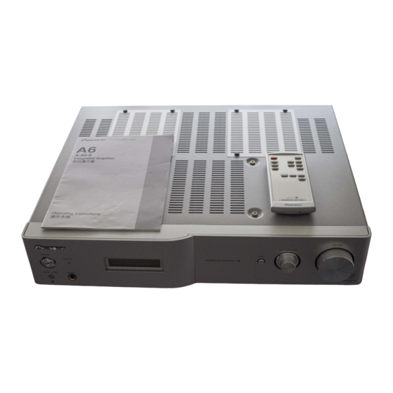
Page 70: Panel Facilities
8. PANEL FACILITIES Front panel POWER INPUT SELECTOR dial Selects an input source. Standby indicator MASTER VOLUME Character display Remote sensor DIRECT Press to switch the Direct listening feature on PHONES jack or off. Use to connect headphones (when connected, there is no sound output from speakers). - Page 71 Remote control Switches the amplifier between standby and on. VOLUME +/- Use to set the listening volume. MUTE Mutes/unmutes the sound S. RETRIEVER (A9 Only) Press to switch the Sound Retriever on/off DIMMER Dims or brightens the display (or switches the backlight off).