Table of Contents
Advertisement
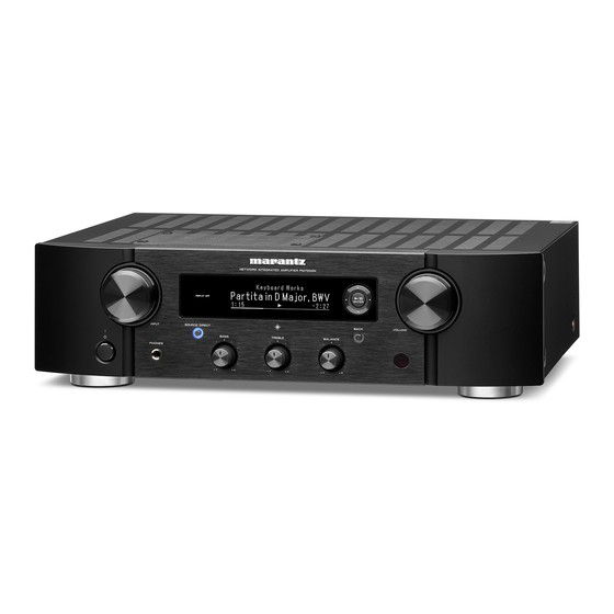
Network Integrated Amplifier
PM7000N
• For purposes of improvement, specifications and design are subject to change without notice.
• Please use this service manual when referring to the operating instructions without fail.
• Some illustrations used in this service manual are slightly different from the actual product.
Service Manual
Click here!
On-line service parts list
https://dmedia.soundunited.com/documents/details/26287
ONLINE PARTS LIST
(P5)
WEB owner's manual
NA:
http://manuals.marantz.com/PM7000N/NA/EN/index.php
EU:
http://manuals.marantz.com/PM7000N/EU/EN/index.php
JP:
http://manuals.marantz.com/PM7000N/JP/JA/index.php
Upload is planned for the time of a future press release.
BEFORE SERVICING THIS UNIT
ELECTRICAL
MECHANICAL
REPAIR INFORMATION
UPDATING
Confidential
Ver. 1
Advertisement
Table of Contents

Related Manuals for Marantz PM7000N


Summary of Contents for Marantz PM7000N
- Page 1 Service Manual Ver. 1 Network Integrated Amplifier PM7000N Click here! On-line service parts list https://dmedia.soundunited.com/documents/details/26287 ONLINE PARTS LIST (P5) WEB owner’s manual http://manuals.marantz.com/PM7000N/NA/EN/index.php http://manuals.marantz.com/PM7000N/EU/EN/index.php http://manuals.marantz.com/PM7000N/JP/JA/index.php Upload is planned for the time of a future press release. BEFORE SERVICING THIS UNIT...
- Page 2 BEFORE SERVICING THIS UNIT SAFETY PRECAUTIONS NOTE FOR SCHEMATIC DIAGRAM HANDLING THE SEMICONDUCTOR AND OPTICS ONLINE PARTS LIST Accessing the Parts List Searching Part Numbers or Ref. Numbers NOTE FOR PARTS LIST SERIAL NUMBER Serial Number Organization SKU Code of this Unit POST-SERVICE PRECAUTIONS Initializing this Unit...
-
Page 3: Safety Precautions
SAFETY PRECAUTIONS The following items should be checked for continued protection of the customer and the service technician. Leakage current check Before returning the set to the customer, be sure to carry out either (1) a leakage current check or (2) a line to chassis resistance check. If the leakage current exceeds 0.5 milliamps, or if the resistance from chassis to either side of the power cord is less than 460 kohms, the set is defective. -
Page 4: Note For Schematic Diagram
NOTE FOR SCHEMATIC DIAGRAM WARNING: Parts indicated by the z mark have critical characteristics. Use ONLY replacement parts recommended by the manufacturer. CAUTION: Before returning the set to the customer, be sure to carry out either (1) a leakage current check or (2) a line to chassis resistance check. -
Page 5: Note For Parts List
ONLINE PARTS LIST (P5) FRONT INPUT VIDEO F.CNT S.CNT DIGITAL WEB owner’s manual 943203500730S http://manuals.marantz.com/AAAAA/NA/EN/index.php http://manuals.marantz.com/AAAAA/EU/EN/index.php Search Result(s) Found - 10 http://manuals.marantz.com/AAAAA/AP/ZH/index.php Upload is planned for the time of a future press release. DIODE, RECTIFIER, SMPS D9001 943203500730S CVD1N4007SL AXIAL... - Page 6 The 14-digit serial number that contains the code of the manufacturing plant and the manufacturing date. 14 digits Factory Manufactured Cumulative Year, month code code serial number The last Month 2digit of year (01 ~ 12) SKU Code of this Unit Product SKU SKU Code PM7000N/U1B PM7000N/N1B PM7000N/N1SG PM7000N/FN...
-
Page 7: Initializing This Unit
POST-SERVICE PRECAUTIONS Initializing this Unit Make sure to initialize this unit after replacing the microcomputer or any peripheral equipment, or the Use network initialization mode to initialize the network related settings. PCB. 1. While the power is On, hold down buttons "POWER" and "BACK" for at least 3 seconds. 2. -
Page 8: Schematic Diagrams
ELECTRICAL SCHEMATIC DIAGRAMS PRINTED CIRCUIT BOARDS SCH01 MCU DIGITAL, AMP, WIRE FIXED A, WIRE FIXED B, WIRE FIXED C, SPK SCH02 DIR MAIN, SMPS SCH03 PLD PHONO, WIRE FIXED D, FRONT, VOLUME, VOLUME ENCODER, HEADPHONE, SCH04 NETWORK SELECTOR ENCODER SCH05 MAIN LEVEL DIAGRAM SCH06 AMP SPK SCH07 PHONO... - Page 9 SCHEMATIC DIAGRAMS SCH01 MCU P3V3_UCOM P3V3_D MCU PART + 5V_LEGO +5V_LEGO P3V3_UCOM L101 220ohm /2200m A CN103 CN103 SMAW 200-07 P3V3_UCOM P5V_NET DGND P3V3_D D 101 +3.3V_D TO BN703 FD LL4148 DGND L102 P3V3_UCOM +5V_LEGO P5V_NET 220ohm /2200m A P5V_D _USB +5V_LEGO IC101 D GND...
- Page 10 SCH02 DIR DIR PART + 5V_D AC_GND + 5V_D AC P3V3_UCOM + 5V_D AC_GND + 5V_D AC P3V3_D P3V3_UCOM L106 P3V3_D _AUD IO P3V3_D TO A5 220ohm /2200m A P1V8_D P3V3_D _AUD IO P5V_AUD IO D GND AGND + 7.5V Q110 -7.5V RT 1P141C...
- Page 11 SCH03 PLD PLD PART L110 P3V3_D _PLD P3V3_D 220ohm /2200m A TO A4 GND_D D GND C356 50V/0.1uF P1V8_D C357 50V/0.1uF PLD _CONF_T MS R390 OPEN PLD _CONF_T D I PLD _CONF_T CK PLD _CONF_T D O R393 OPEN D IR2_PLD _MCK CS2K_PLD _MCK D IR2_PLD _MCK D IR2_PLD _PBCK...
- Page 12 SCH04 NETWORK FROM LEGO MODULE NETW ORK PART 42 Pin CONNECTOR 80 Pin CONNECTOR CN111 CJP42GA370ZU CN110 CJP80GA370ZU P3V3_UCOM L115 LEGO5V P5V_NET 120R/200m A P5V_D _USB R548 D GND Q114 R547 Q115 R546 T PC6111 C359 50V/0.1uF K RC102S TO A3 SW 105 NET3.3V L116...
- Page 13 SCH05 MAIN CN706 CN715 TO BN1506 TO BN1515 C777 R941 TO_TONE TO_TONE CN706 63V/220uF-RA2 0.25W /22 CN715 J700 R837 TO_PH ONO 4.7K -AX J701 Q757 Q741 BN705 K SA992F KSA992F +15V Q749 KSC1845F -15V R717 PHONO L-OUT Q759 Q755 4.7K -AX K T C3198Y Q747 K SC1845F...
- Page 14 SCH06 AMP SPK FROM MAIN TRANSFORMER J1264 MAIN AMP D 1306 CVD D 30X BN20 J1317 J1266 * VERSION OPTION J1359 J1316 J1314 J1362 VER. C1371 C1372 FROM_MAIN TRANS CCMP2A103JS13T CCMP2A103JS13T AGND Q1311 G1301 OPEN OPEN Q1303 J1265 CN1310 KT C3206Y GND-TERMINAL CJP03GA90ZY R1307...
- Page 15 SCH07 PHONO PHONO * VERSION OPTION C1209 R1223 C1201 R1201 L1201 VER. 3300pF(M) C1202 R1202 L1202 CCMP2B221KS17T 6.8k CLZBLM18H G102SN1D OPEN OPEN R1233 OPEN R1217 C1219 100-AX OPEN R1225 C1213 6.8K -AX 25V/22uF-RA2 Q1205 100V/0.039uF C1215 100-AX CN1205 VERSION OPTION 100V/0.01uF J1283 C1261...
- Page 16 SCH08 FRONT WF1501 TO WF1504 OLED<=>TONE FRONT CN1503 Q1507 RT 1P141C Q1508 RT 1P141C W F1501 +3.3V CJP23GB113ZY DGND INPUT SELECT DGND SEL_AD SEL_INT TO BN1503 BN1503 SEL_INT VOLUME SEL_AD CN1504 DGND +3.3V DGND DGND +3.3V DGND TO CN1503 R1515 R1514 R1513 R1512...
- Page 17 SCH09 SMPS R1842 NC(3216) F1800 NT1800 R1821 CX1800 B1800 CY1801 AC250V/T1AL OPEN 47(3216) BFD3580 104/275VAC C1821 R1822 1KV/102 B1821 47(3216) ST_+DC LF1800 R1801 BD1800 BFS3550 RX1800 R1806 R1803 UU1014 1.3MF ABS210 (R-TYPE) 1.3M(3216) 20mH(MIN) 5.1MF(3216) 33K(3216) (3216) CN1800 (1000V/2A) ST_+6.8V YW396-03AV C1802 T1800...
- Page 18 PRINTED CIRCUIT BOARDS DIGITAL, AMP, WIRE FIXED A, WIRE FIXED B, WIRE FIXED C, SPK Lead-free Solder When soldering, use the Lead-free Solder (Sn-Ag-Cu). AMP (A Side) AMP (B Side) WIRE FIXED A (A Side) DIGITAL (A Side) DIGITAL (B Side) C247 C238 C240...
- Page 19 MAIN, SMPS MAIN (A Side) MAIN (B Side) SMPS (A Side) JK702 R885 R904 R942 SPK_RELAY C815 HP_RELAY IC716 +5V_LEGO DGND DGND +5V_USB D766 IC701 +5V_USB RC_GND D765 RC_D_IN/OUT C826 C819 C722 A_PW_CONT C713 D_PW_CONT DGND C714 ST_+6.8V C827 +12V +12V DGND DGND...
- Page 20 PHONO, WIRE FIXED D, FRONT, VOLUME, VOLUME ENCODER, HEADPHONE, SELECTOR ENCODER FRONT (A Side) FRONT (B Side) VOLUME (A Side) VOLUME (B Side) PHONO (A Side) PHONO (B Side) WF1503 MI ICT FCT1 FCT2 J1527 1.AGND 2.AK4490_L_OUT- 3.AK4490_L_OUT+ BK101 4.AGND 5.AK4490_R_OUT+ 6.AK4490_R_OUT- 7.AGND...
-
Page 21: Level Diagram
LEVEL DIAGRAM PM7000N LEVEL DIAGRAM 60W 8ohm 21.9V (26.8dB) +23.16dB CD etc 200mV (-14dB) +17.7dB Digital in -22.5dBFS(PCB) , -18.6dBFS(DSD) RECODER OUTPUT 200mV (-14dB) SUB WOOFER OUTPUT(VOL POSITION 54) 220mV (-13.15dB) MM 2mV (-54.0dB) -
Page 22: Block Diagram
BLOCK DIAGRAM PM7000N Block Diagram RC-5 AUDIO UNIT Digital UNIT Phono EQ Amp IN/OUT COAX OPT1 OPT2 with JFET input PHONO Relay Current Feedback Amplifier -6dB with HDAM-SA3 GND_D GND_CHASSIS HDAM + Relay Power Amp HDAM-SA2 buffer +24.0dB Volume IC... -
Page 23: Power Diagram
POWER DIAGRAM... -
Page 24: Wiring Diagram
WIRING DIAGRAM W I R I N G D I A G R A M * FFC LIST Location (Ref.No) PART NUMBER COMMENT FFC1 CWC4F4A11A120A08J 11pin, 1.0mm Pitch, 120mm, A Type SPEAKER PCB FFC2 CWC4F4A23A200A08J 23pin, 1.0mm Pitch, 200mm, A Type CUP13074Z_2 c t i CN1320 (5PIN, WAFER) - Page 25 SEMICONDUCTORS Only major semiconductors are shown, general semiconductors etc. are omitted to list. The semiconductor which described a detailed drawing in a schematic diagram are omitted to list. 1. IC's R5F5631FDDFB (DIGITAL : IC104) Nor- Opti- Net- Symbol Pin Name Description work STBY...
- Page 26 Nor- Opti- Net- Nor- Opti- Net- Symbol Pin Name Description Symbol Pin Name Description work work STBY STBY STBY STBY STBY STBY P82/TXD10/RMII0_TXD1/MMC_ 111 PE0/SSLB2-B "NET3.3V" Power Supply Control P82/TXD10 NJU72322 Volume Control D4-A 112 P64/(D3[A3/D3])*1 Recorder output mute (Relay on/off =H/L) 64 P81/RXD10/ET0_ETXD0 P81/RXD10 DIR2 (LC89091JA) General Purpose Signal Input...
- Page 27 *For adjustable version only. Figure 1. Typical Application Circ Figure 1. Typical Application Circuit PCF8574APWR (DIGITAL : IC103) NCP380 (DIGITAL : IC119) ILIM* PAD1 ILIM* ILIM* PAD1 FLAG FLAG FLAG Terminal Function TSOP−5 UDFN6 TSOP−6 FLAG FLAG Pin Functions (Top view) TYPE DESCRIPTION NAME...
- Page 28 AK4458VN 40 +105 C (Exposed pad is connected to ground) 40 +85 C (Exposed pad is open) 48-pin QFN (0.5mm pitch) AKD4458 Evaluation Board for AK4458 AK4458VN (DIGITAL : IC113) No. Pin Name I/O Function PD State CAD0_I2C Chip Address 0 Pin in I2C Bus serial control mode Pin Configurations Chip Select Pin in 3-wire serial control mode Hi-Z...
- Page 29 [AK4458] PCM9211 PCM9211 (DIGITAL : IC107) AK4458VN BLOCK DIAGRAM 4. Block Diagram and Functions www.ti.com SBAS495 – JUNE 2010 PIN CONFIGURATIONS PT PACKAGE LDOE TVDD VDD18 DVSS AVDD AVSS LQFP-48 (TOP VIEW) Bias BICK/DCLK DATT AOUTL1P LRCK/DSDL1 Soft Mute Interpolator AOUTL1N SDTI1/DSDR1 ERROR/INT0...
- Page 30 LC89091JA (DIGITAL : IC108) DESCRIPTION NAME TOLERANT RXIN1 Biphase signal, input 1, built-in coaxial amplifier VDDRX – – Power supply, 3.3 V (typ.), for RXIN0 and RXIN1. RXIN0 Biphase signal, input 0, built-in coaxial amplifier GNDRX Ground, for RXIN Oscillation circuit input for crystal resonator or external XTI clock source input(5) Oscillation circuit output for crystal resonator AGND –...
- Page 31 NJU72750A (MAIN : IC701, IC707) SSC3S121 (SMPS : IC1800) FB/OLP BLOCK DIAGRAM Pin Function Startup No. Symbol Function No. Symbol Function UVLO VREG positive power supply terminal DATA IC control data input Brown-in/out, InA1 Ach input1 CLOCK IC control clock input InB1 Bch input1 PWM OSC...
- Page 32 2. FL DISPLAY MXS4035A (WF1502) MXS4035A IO Interfaces...
- Page 33 3. Remote Code Table RC004PM_Layout PM7000N (RC-5) AMP MODE Key Name Code Layout Name System Command Extension Layout CD MODE AMP MODE (Default) Pre-Main/Others CD POWER CD POWER CD POWER CD Player CD (Mode switching) CD (Mode switching) CD (Mode switching)
- Page 34 AMP_Extension PM7000N (RC-5) CD MODE Layout Name Layout Name System Command Extension System Command Extension Power On CD POWER Power Off CD (Mode switching) MUTE ON AMP (Mode switching) MUTE OFF AMP POWER Input Select REV INTERNET RADIO OPTICAL (Toggle)
- Page 35 MECHANICAL DISASSEMBLY Flowchart 1. FRONT ASSY 2. DIGITAL ASSY 3. PHONO PCB 4. HEAT SINK ASSY 5. SPK PCB 6. MAIN PCB 7. SMPS PCB 8. TRANS EXPLODED VIEW PACKAGING VIEW...
- Page 36 DISASSEMBLY Flowchart • Remove each part following the flow below. • Reassemble the removed parts in the reverse order. • Read "SAFETY PRECAUTIONS" before reassembling the removed parts. • If wire bundles are removed or moved during adjustment or part replacement, reshape the wires after completing the work. Failure to shape the wires correctly may cause problems such as noise. • See "EXPLODED VIEW" TOP COVER FRONT ASSY DIGITAL ASSY SMPS PCB DISASSEMBLY DISASSEMBLY DISASSEMBLY 1. FRONT ASSY 2. DIGITAL ASSY 7. SMPS PCB and "EXPLODED VIEW" and "EXPLODED VIEW" and "EXPLODED VIEW" FRONT PCB DIGITAL PCB SMPS PCB Ref. No. of EXPLODED VIEW : P 1 Ref. No. of EXPLODED VIEW : P 6 Ref. No. of EXPLODED VIEW : P 11 VOLUME PCB MODULE Ref. No. of EXPLODED VIEW : P 2 Ref. No. of EXPLODED VIEW : P 17 SELECTOR ENCODER PCB Ref. No. of EXPLODED VIEW : P 3 PHONO PCB VOLUME ENCODER PCB DISASSEMBLY...
-
Page 37: Front Assy
• For the shooting direction of each photos used in this manual, see the photo below. • A, B, C and D in the photo below indicate the shooting directions of photos. Proceeding : TOP COVER → FRONT ASSY • The photographs with no shooting direction indicated were taken from the top of the unit. (1) Remove the screws. • Photos of PM7000N N1B are used in this manual. The viewpoint of each photograph (Shooting direction : X) [View from the top] ↓Shooting direction: B↓ View from the bottom (2) R emove the screws. Cut the wire clamp, then remove the connector. Remove the TAPE. Remove the FFC. ↓Shooting direction: B↓... -
Page 38: Digital Assy
2. DIGITAL ASSY 3. PHONO PCB Proceeding : TOP COVER → DIGITAL ASSY Proceeding : TOP COVER → DIGITAL ASSY → PHONO PCB (1) R emove the screws. Remove the TAPE. Remove the connector. Remove the FFC. (1) R emove the screws. Remove the connector. Remove the PCB HOLDER. ↓Shooting direction: B↓ TAPE CN103 CN1205 CN102 PCB HOLDER x2 TAPE CN105 ↑Shooting direction: A↑... -
Page 39: Heat Sink Assy
4. HEAT SINK ASSY 6. MAIN PCB Proceeding : TOP COVER → FRONT ASSY → DIGITAL ASSY → PHONO PCB Proceeding : TOP COVER → FRONT ASSY → DIGITAL ASSY → PHONO PCB → HEAT SINK ASSY → HEAT SINK ASSY → MAIN PCB (1) R emove the screws. Cut the wire clamp, then remove the connector. -
Page 40: Exploded View
EXPLODED VIEW https://dmedia.soundunited.com/documents/details/26287 Parts List : PM7000N EXPLODED VIEW WARNING: Parts marked with this symbol z have critical characteristics. Use ONLY replacement parts recommended by the manufacturer. - Page 41 PACKAGING VIEW https://dmedia.soundunited.com/documents/details/26287 Parts List : 17-1 17-2 17-3 17-4 17-5 17-6 17-7 17-8 17-9 17-10 17-11 17-12 17-13 17-14 UK plug (UK Only)
-
Page 42: Troubleshooting
REPAIR INFORMATION TROUBLE SHOOTING SPECIAL MODE 1. The power cannot be turned on Special mode setting button (STANDBY LED is not lit(STANDBY MODE)) 1. Selecting the Mode1 for Service-related 2. The power cannot be turned on 1-1. Version Display Mode (STANDBY LED is lit→light flashes) 1-2. - Page 43 TROUBLE SHOOTING 1. The power cannot be turned on (STANDBY LED is not lit(STANDBY MODE)) Check insertion of the connector of the SMPS PCB. Check insertion of the connector of the DIGITAL PCB. No voltage Failure of the SMPS PCB. No voltage Check the [CN1800 : 1pin ST+6.8V] of SMPS PCB.
- Page 44 3. STANDBY LED flashes while using the unit 5.1 DIGITAL BLOCK Power Supply Voltage Abnormalities (Protection circuit becomes activated) "2. The power cannot be turned on Check connector is properly attached. If there Check insertion of each connector. (STANDBY LED is lit → light flashes)"...
- Page 45 6. No Audio Output during USB File Playback (USB-A input), File Playback on a Server or Internet Radio and Bluetooth Playback Before testing circuit operation, check if the file to be played back is in a supported format and network settings are correct. Check that the digital audio signal is output from HEOS MODULE during audio file and streaming play- DIGITAL PCB back.
- Page 46 7. OLED 8. No Remote Control Reception 6.1. OLED is not lit Check that you are using a [RC004PM] remote control and replace the batteries. Check that the connector between MAIN PCB and DIGITAL PCB is properly attached. Check that the 11P FFC cable connecting DIGITAL PCB and FRONT PCB is properly inserted. Check that the 23P FFC cable connecting DIGITAL PCB and FRONT PCB is properly attached.
-
Page 47: Special Mode Setting Button
SPECIAL MODE Special mode setting button b No. 1 : Insert the AC plug while pressing "A" button, and wait for more than 3 seconds. b No. 2, 3 : Insert the AC plug while pressing "A" and "B" buttons together, and wait for more than 3 seconds. b No. - Page 48 1. Selecting the Mode1 for Service-related 1.1. Actions r All Device DPMS Update Selecting Each Mode. 1.2. Starting up Insert the AC plug while pressing "POWER" button, and wait for more than 3 seconds. Executes an update for the entire device via DPMS. Select the desired mode using the "CURSOR f / d "...
-
Page 49: Version Display Mode
1-1. Version Display Mode 1-1.1. Actions r HEOS Version o Restore Version information is displayed when the device is started in this mode. 1-1.2. Starting up Insert the AC plug while pressing "POWER" button, and wait for more than 3 seconds. Select the "Version Check"... -
Page 50: Protection History Display Mode
• Display for detection of short circuits in analog and DDFA-related power supplies 1-2. IR Control Test This function is used to check IR control operations. Since this mode is only for production/development, the detailed information is not provided. Cause : Completely destroyed circuit assumed 1-3. - Page 51 1-4. All Device DPMS Update mode 1-6. Initialize Standard updates are now performed through OTA. Initializes all MCU and network module backup data. "6. Normal Firmware Update Method from OTA (NETWORK MODULE)" NOTE : If initialization is executed in Network Off mode, cancel Network off mode then reset the Net- work.
- Page 52 2. Factory Initialization Mode 4. Network Function Reset Initialize backup data of the MCU. Initializes network settings. 4.1. Actions 2.1. Starting up The following items are initialized. 1. Insert the AC plug while pressing buttons "SOURCE DIRECT" and "BACK" together, and wait for more (1) Network setup than 3 seconds.
- Page 53 (3) When saving of the log package fails, "USB FAILED" appears in the display for 5 seconds, regardless 5. Selecting the Mode2 for Service-related of whether the upload to the server was successful. Selecting Each Mode. 5.1. Starting up While the power is on, hold down buttons "POWER" and "ENTER" for at least 3 seconds. (1) "LEGO Log Capture Mode"...
-
Page 54: Adjustment Procedure
ADJUSTMENT 1. DC Offset Voltage Adjustment 2. Idling Current Adjustment 1. Preparation Adjusting Procedure (1) Prepare a DC voltmeter. Digital Voltmeter Digital Voltmeter (2) Place the unit under normal usage conditions, away from highly ventilated areas such as next to an air conditioning machine or electric fan. - Page 55 UPDATING PROCEDURE AFTER REPLACING THE PCB. PROCEDURE AFTER REPLACING THE U-COM, ETC. FIRMWARE UPDATE PROCEDURE 1. Items necessary for update 2. Update preparation with a USB flash drive (NETWORK MODULE) 3. Update method when the MAIN PCB or network module is replaced (Using a USB flash drive NETWORK MODULE) 4.
- Page 56 PROCEDURE AFTER REPLACING THE PCB. PROCEDURE AFTER REPLACING THE U-COM, ETC. The procedure after replacing the printed circuit boards is as follows. The procedure after replacing the MCU (microprocessor) is as follows. (1) Change the resistor for setting the region. Implement the update method when the DIGITAL PCB or module is replaced.
-
Page 57: Firmware Update Procedure
Update download file when the firmware is updated (Two files, "HW component" and "Network component") Download from SDI Model Name Model Area For HW component For Network component PM7000N U North America (U) Product ID : 100200140100 PM7000N N Europe (N) Product ID : 100200140200 DPMS_PM7000NALL_LEGO_xxx.zip... - Page 58 2. Update preparation with a USB flash drive (NETWORK MODULE) You can update the firmware by downloading the latest version with USB flash drive. 2.1. Connecting to the USB flash drive (1) Preparation • Windows PC • USB flash drive format : Prepare a USB flash drive formatted in FAT16 or FAT32. b We recommend a USB flash drive that has an LED installed.
-
Page 59: Start The Update
3. Update method when the MAIN PCB or network module is replaced (Using a USB flash drive NETWORK MODULE) 3.1. File structure on USB flash drive (5) USB Update starts automatically. The power indicator lights up in red. MAIN PCB or network module is replaced onto the USB flash drive in the following structure. Display during USB update After unzipping the files, store them in the root of the same USB flash drive. - Page 60 4. Update Method for Service Region Settings (NETWORK MODULE) Copy the Service Region Settings from the USB flash drive to this unit. (5) Copy the files created on the USB flash drive. 4.1. Creating a Service Region Settings file (1) Click [Start button] - [Accessories] - [notepad] on the PC to launch the notepad. copy to USB flash drive (2) Enter "TEXT".
- Page 61 5. Normal Firmware Update Method from USB Flash Drive (NETWORK MODULE) 5.1. File structure on USB flash drive (1) Press the power operation button to turn off the power, and remove the AC plug from the socket. (2) Insert the AC plug while pressing buttons "SOURCE DIRECT" and "ENTER" together, and wait for Copy the normal update files onto the USB flash drive in the following structure.
-
Page 62: Network Connection
6. Normal Firmware Update Method from OTA (NETWORK MODULE) 6.2. Check and update the firmware Download the latest firmware from our website and update the firmware. Check if there is a firmware update available. It is also possible to check approximately how long the ---Cautions on Firmware Update--- update will take. - Page 63 7. About the error codes (NETWORK MODULE) See the table below for details on error codes and solutions when updating the firmware. Device ID table Error codes are displayed in 4 digits, : DeviceID, : ErrorCode). YYXX Device ID ( YY ) Device Name Display General...
- Page 64 Copyright © 2019 D&M Holdings Inc. All Rights Reserved.
Need help?
Do you have a question about the PM7000N and is the answer not in the manual?
Questions and answers