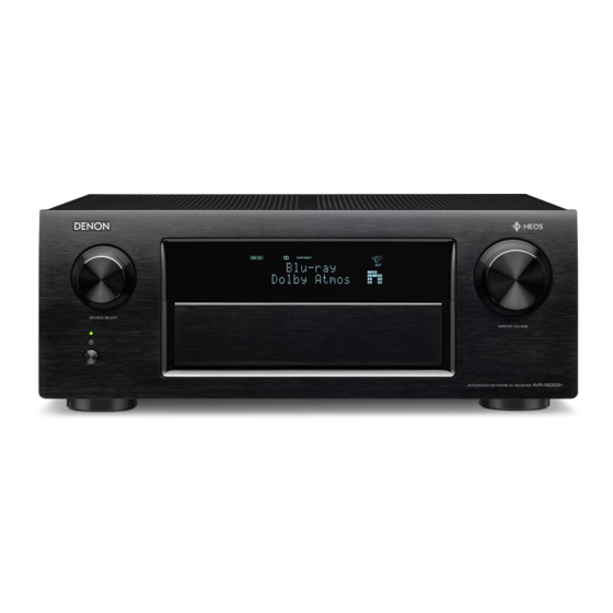
Denon AVR-X6300H Service Manual
Integrated network av receiver
Hide thumbs
Also See for AVR-X6300H:
- Quick start manual (11 pages) ,
- Owner's manual (342 pages) ,
- Quick start manual (15 pages)
Table of Contents
Advertisement
Quick Links
INTEGRATED NETWORK AV RECEIVER
AVR-X6300H
• For purposes of improvement, specifications and design are subject to change without notice.
• Please use this service manual with referring to the operating instructions without fail.
• Some illustrations using in this service manual are slightly different from the actual set.
Service Manual
Click here!
On-line service parts list
http://dmedia.dmglobal.com/Document/DocumentDetails/23012
Online Parts List
(P5 to P7)
WEB owner's manual
http://manuals.denon.com/AVRX6300H/NA/EN/index.php
http://manuals.denon.com/AVRX6300H/EU/EN/index.php
CAUTION IN SERVICING
ELECTRICAL
MECHANICAL
REPAIR INFORMATION
UPDATING
Appendix
Please refer to the MODIFICATION NOTICE.
Ver. 6
Advertisement
Table of Contents

Related Manuals for Denon AVR-X6300H


Summary of Contents for Denon AVR-X6300H
- Page 1 Service Manual Ver. 6 INTEGRATED NETWORK AV RECEIVER Click here! AVR-X6300H On-line service parts list http://dmedia.dmglobal.com/Document/DocumentDetails/23012 Online Parts List (P5 to P7) WEB owner’s manual http://manuals.denon.com/AVRX6300H/NA/EN/index.php http://manuals.denon.com/AVRX6300H/EU/EN/index.php CAUTION IN SERVICING ELECTRICAL MECHANICAL REPAIR INFORMATION UPDATING Appendix • For purposes of improvement, specifications and design are subject to change without notice. Please refer to the MODIFICATION NOTICE.
-
Page 2: Caution In Servicing
CAUTION IN SERVICING SAFETY PRECAUTIONS NOTE FOR SCHEMATIC DIAGRAM NOTE FOR PARTS LIST INSTRUCTIONS FOR HANDLING SEMICONDUCTORS AND OPTICAL UNIT CAUTION IN SERVICING. Initializing This Unit JIG FOR SERVICING... -
Page 3: Safety Precautions
SAFETY PRECAUTIONS ◎ Make a safety check after servicing! The following items should be checked for continued protection of the customer and the service Check that all screws, parts and wires removed or disconnected when servicing have been put back technician. -
Page 4: Note For Schematic Diagram
NOTE FOR SCHEMATIC DIAGRAM WARNING: Parts indicated by the z mark have critical characteristics. Use ONLY replacement parts recommended by the manufacturer. CAUTION: Before returning the set to the customer, be sure to carry out either (1) a leakage current check or (2) a line to chassis resistance check. - Page 5 Online Parts List Accessing the Parts List Logging in to New SDI and Accessing the Parts List (1) Click the URL link on the cover of the service manual. (1) Access New SDI from the URL below. Examples of display <http://dmedia.dmglobal.com>...
-
Page 6: Revision History
Accessing the Part List from the Model Asset Screen Downloading the Parts List as an Excel File (1) Display Model Asset from New SDI. (1) Displays the Parts List. Click the Download icon. (2) Click the section displayed as ▼ Link to Part Lists under the model name. NOTE : If the ▼... - Page 7 Searching Part Numbers or Ref. Numbers You can search a Parts List for part numbers or Ref. numbers. (1) Enter the part number or Ref. number in the search window of the Parts List, and press the search button. (2) The search results are displayed. The name of the sheet in which the search part is used and the part’s line are displayed.
-
Page 8: Initializing This Unit
CAUTION IN SERVICING. Initializing This Unit Make sure to initialize this unit after replacing the microcomputer or any peripheral equipment, or the digital PCB. 1. Press the power button to turn off the power. 2. While holding down buttons "CURSOR d " and "CURSOR f " simultaneously, press the power button to turn on the power. -
Page 9: Schematic Diagrams
ELECTRICAL SCHEMATIC DIAGRAMS SCH35_FLD SCH01_DIGITAL CONNECT PRINTED CIRCUIT BOARDS SCH02_MAIN CPU SCH03_EXPANDER DIGITAL SCH04_AUDIO PLD AUDIO VIDEO, FRONT HDMI USB, CONNECT-1, SCH05_DIR DA SUPPLY CONNECT-2, CONNECT-4 SCH06_ADI DSP1 DAC, L AMP CONNECT, R AMP CONNECT, FRONT SCH07_ADI DSP2 SPEAKER, HEIGHT2 SP, HP, P.SW SCH08_ADI DSP3 AMP1, AMP2, SMPS, 232C PHONO, CONNECT-3, SCH09_ADI DSP4... - Page 10 SCHEMATIC DIAGRAMS All Ref.No. has been described in the parts list are four digits. SCH01_DIGITAL CONNECT But there are less than four digits of printed Ref.No. on the PCB, and they have become four digits after the header by adding "0" in the parts list. N6012 N6011 N6010...
- Page 11 All Ref.No. has been described in the parts list are four digits. SCH02_MAIN CPU But there are less than four digits of printed Ref.No. on the PCB, and they have become four digits after the header by adding "0" in the parts list. TO 3C TO 2C TO 1C...
- Page 12 All Ref.No. has been described in the parts list are four digits. SCH03_EXPANDER But there are less than four digits of printed Ref.No. on the PCB, and they have become four digits after the header by adding "0" in the parts list. TO 4C TO 5C TO 6C...
- Page 13 All Ref.No. has been described in the parts list are four digits. SCH04_AUDIO PLD But there are less than four digits of printed Ref.No. on the PCB, and they have become four digits after the header by adding "0" in the parts list. TO 3E R1294 TO A1...
- Page 14 All Ref.No. has been described in the parts list are four digits. SCH05_DIR DA SUPPLY But there are less than four digits of printed Ref.No. on the PCB, and they have become four digits after the header by adding "0" in the parts list. TO A0 TO A5 TO D7...
- Page 15 All Ref.No. has been described in the parts list are four digits. SCH06_ADI DSP1 But there are less than four digits of printed Ref.No. on the PCB, and they have become four digits after the header by adding "0" in the parts list. TO E6 TO D1 TO 0F...
- Page 16 All Ref.No. has been described in the parts list are four digits. SCH07_ADI DSP2 But there are less than four digits of printed Ref.No. on the PCB, and they have become four digits after the header by adding "0" in the parts list. TO E7 TO D2 TO F0...
- Page 17 All Ref.No. has been described in the parts list are four digits. SCH08_ADI DSP3 But there are less than four digits of printed Ref.No. on the PCB, and they have become four digits after the header by adding "0" in the parts list. TO E8 TO D3 TO F2...
- Page 18 All Ref.No. has been described in the parts list are four digits. SCH09_ADI DSP4 But there are less than four digits of printed Ref.No. on the PCB, and they have become four digits after the header by adding "0" in the parts list. TO E9 TO D4 TO C3...
- Page 19 All Ref.No. has been described in the parts list are four digits. SCH10_HDMI SUPPLY But there are less than four digits of printed Ref.No. on the PCB, and they have become four digits after the header by adding "0" in the parts list. DIGITAL TO J9 DGND...
- Page 20 All Ref.No. has been described in the parts list are four digits. SCH11_DECODER But there are less than four digits of printed Ref.No. on the PCB, and they have become four digits after the header by adding "0" in the parts list. CEC5V DV5V HDMI...
- Page 21 All Ref.No. has been described in the parts list are four digits. SCH12_HDMI SW2 But there are less than four digits of printed Ref.No. on the PCB, and they have become four digits after the header by adding "0" in the parts list. CEC5V CEC3.3V Q2605...
- Page 22 All Ref.No. has been described in the parts list are four digits. SCH13_HDMI SW1 But there are less than four digits of printed Ref.No. on the PCB, and they have become four digits after the header by adding "0" in the parts list. TO HDMI SUPPLY TO 8U-310215(10/19)
- Page 23 All Ref.No. has been described in the parts list are four digits. SCH14_IP OSD But there are less than four digits of printed Ref.No. on the PCB, and they have become four digits after the header by adding "0" in the parts list. DV5V DV3.3V L2815...
- Page 24 All Ref.No. has been described in the parts list are four digits. SCH15_IP OSD DDR But there are less than four digits of printed Ref.No. on the PCB, and they have become four digits after the header by adding "0" in the parts list. TO IP/OSD TO IP/OSD TO IP/OSD...
- Page 25 All Ref.No. has been described in the parts list are four digits. SCH16_VIDEO PLD But there are less than four digits of printed Ref.No. on the PCB, and they have become four digits after the header by adding "0" in the parts list. .PO8KI_Y5/R1 VP3.3V .PO8KI_C10/G2...
- Page 26 All Ref.No. has been described in the parts list are four digits. SCH17_HDMI TX But there are less than four digits of printed Ref.No. on the PCB, and they have become four digits after the header by adding "0" in the parts list. CEC_STBY5V CEC_STBY3.3V CEC5V...
- Page 27 All Ref.No. has been described in the parts list are four digits. SCH18_NET MODULE CONNECT But there are less than four digits of printed Ref.No. on the PCB, and they have become four digits after the header by adding "0" in the parts list. NET5V L8005 TO DIGITAL...
- Page 28 All Ref.No. has been described in the parts list are four digits. SCH19_CY920(all OPEN) But there are less than four digits of printed Ref.No. on the PCB, and they have become four digits after the header by adding "0" in the parts list. TO E0 TO 7H TO B5...
- Page 29 All Ref.No. has been described in the parts list are four digits. SCH20_AUDIO/VIDEO CONNECT But there are less than four digits of printed Ref.No. on the PCB, and they have become four digits after the header by adding "0" in the parts list. "SCHEMATIC DIAGRAMS_Appendix"...
- Page 30 CLOCK DATA SEL_CLK PREOUT_C R3277 OPEN INGND VOLMUTE SEL_DATA AMPIN_FL R3278 C3252 100/16 VOL_DATA INGND R8172 C3245 100/16 R3279 AMPIN_SL AVR-X6300H:OPEN INGND R3288 AMPIN_SBL C3255 100/16 INGND C3254 100/16 AMPIN_H2L R3289 EXT_FL INGND EXT.FL C3215 AMPIN_H3L R3290 R3215 R3237 OPEN...
- Page 31 OPEN OPEN H1R/H1L R8187 OPEN R8188 OPEN R3554 C3556 R3523 S3510 OPEN OPEN C3533 OPEN OPEN R3571 OPEN OPEN .PREOUT_H1L AVR-X6300H C3534 .PREOUT_H2R 10/63 R3524 R3555 C3557 R3572 100K S3511 100K 470P G6J-2P-Y R8189 OPEN H1R/H1L H2R/H2L R8190 OPEN S3511...
- Page 32 All Ref.No. has been described in the parts list are four digits. SCH23_VIDEO SELECTOR But there are less than four digits of printed Ref.No. on the PCB, and they have become four digits after the header by adding "0" in the parts list. TO AUDIO/VIDEO CONNECT TO 8U-210222-1(1/4) C7675...
- Page 33 All Ref.No. has been described in the parts list are four digits. SCH24_CONNECT But there are less than four digits of printed Ref.No. on the PCB, and they have become four digits after the header by adding "0" in the parts list. N5907 TO DIGITAL To_8U-310215_(N6012)
- Page 34 All Ref.No. has been described in the parts list are four digits. SCH25_AMP CONNECT But there are less than four digits of printed Ref.No. on the PCB, and they have become four digits after the header by adding "0" in the parts list. Z5809 STYLE-PIN N5833...
- Page 35 All Ref.No. has been described in the parts list are four digits. SCH26_ZONEDAC ADC But there are less than four digits of printed Ref.No. on the PCB, and they have become four digits after the header by adding "0" in the parts list. "SCHEMATIC DIAGRAMS_Appendix"...
- Page 36 All Ref.No. has been described in the parts list are four digits. SCH27_MAIN DAC But there are less than four digits of printed Ref.No. on the PCB, and they have become four digits after the header by adding "0" in the parts list. "SCHEMATIC DIAGRAMS_Appendix"...
- Page 37 All Ref.No. has been described in the parts list are four digits. SCH28_FRONT HDMI USB But there are less than four digits of printed Ref.No. on the PCB, and they have become four digits after the header by adding "0" in the parts list. R5501 R5502 R5503...
- Page 38 All Ref.No. has been described in the parts list are four digits. SCH29_SMPS But there are less than four digits of printed Ref.No. on the PCB, and they have become four digits after the header by adding "0" in the parts list. B6501 CMD1A834 C6501...
- Page 39 All Ref.No. has been described in the parts list are four digits. SCH30_232C PHONO But there are less than four digits of printed Ref.No. on the PCB, and they have become four digits after the header by adding "0" in the parts list. N3902 N3902 K3901...
- Page 40 All Ref.No. has been described in the parts list are four digits. SCH31_P.AMP1 But there are less than four digits of printed Ref.No. on the PCB, and they have become four digits after the header by adding "0" in the parts list. -61.6V 62.9V 62.3V...
- Page 41 All Ref.No. has been described in the parts list are four digits. SCH32_P.AMP2 But there are less than four digits of printed Ref.No. on the PCB, and they have become four digits after the header by adding "0" in the parts list. D201 R206 C205...
- Page 42 All Ref.No. has been described in the parts list are four digits. SCH33_SPEAKER But there are less than four digits of printed Ref.No. on the PCB, and they have become four digits after the header by adding "0" in the parts list. N6015 N6014_ TO N102-5...
- Page 43 All Ref.No. has been described in the parts list are four digits. SCH34_REG But there are less than four digits of printed Ref.No. on the PCB, and they have become four digits after the header by adding "0" in the parts list. Q6204 F6203 KTC2026...
- Page 44 All Ref.No. has been described in the parts list are four digits. SCH35_FLD But there are less than four digits of printed Ref.No. on the PCB, and they have become four digits after the header by adding "0" in the parts list. N6405 Z6411 OPEN...
- Page 45 PRINTED CIRCUIT BOARDS DIGITAL Lead-free Solder When soldering, use the Lead-free Solder (Sn-Ag-Cu). DIGITAL (A SIDE) B501 DIGITAL UNIT S8001 R3402 63301021520AS R3401 N6201 R6286 N6003 C9040 R6288 R5075 N6011 N6010 8U-310215 R6510 U6505 R6513 R1934 C6507 R6298 R6206 R6282 R3405 B603 N6001...
- Page 46 AUDIO VIDEO, FRONT HDMI USB, CONNECT-1, CONNECT-2, CONNECT-4 AUDIO VIDEO (A SIDE) AUDIO VIDEO (B SIDE) FRONT HDMI USB (A SIDE) FRONT HDMI USB (B SIDE) Z5559 N5560 L5559 8U-210222-5 FRONT HDMI/USB N5501 N5559 R5510 R5509 C5503 R5508 R5507 R5513 D5501 C5502 C5501...
- Page 47 DAC, L AMP CONNECT, R AMP CONNECT, FRONT L AMP CONNECT (A SIDE) L AMP CONNECT (B SIDE) DAC (A SIDE) C7610 C7645 R7542 R7541 R7626 R7625 R7597 R7640 C7603 C7588 R7556 R7570 U7515 C7617 C7644 R7555 R7639 C7602 C7587 R7596 R7569 R7624...
- Page 48 SPEAKER, HEIGHT2 SP, HP, P.SW SPEAKER (A SIDE) HEIGHT2 SP (A SIDE) HEIGHT2 SP (B SIDE) CENTER C6051 K6009 K6008 K6007 K6006 K6005 K6004 K6003 K6002 K6001 K6011 K6010 B6408 B6409 JV17 8U-110206-6 C6059 C6058 C6057 C6056 C6055 C6054 JV221 C6053 C6052 JV94...
- Page 49 AMP1, AMP2, SMPS, 232C PHONO, CONNECT-3, POSISTER, RADIATOR COVER AMP1 (A SIDE) AMP1 (B SIDE) SMPS (A SIDE) SMPS (B SIDE) D6520 N101 R131 J6501 (P=1.9) JV267 JV105 Q111 C6526 C6527 R132 Z106 R101 N102 R130 R6531 JV108 C117 D6519 C6524 Q112 R6528...
-
Page 50: Level Diagram
LEVEL DIAGRAM FRONT ch AVR-X6300H LEVEL DIAGRAM FRONT ch NJU72343 NJU72751 NJU72750 H/POUT NJU72751 NJU72750 SPEAKER LINE + GAIN ADJ. - AK4458 MIC IN + + + AK5358 - - MUTE PRE OUT TO ZONE2 x4pcs TO ZONE3 +30dB 4.24Vrms/8Ω... - Page 51 CENTER / SURROUND ch AVR-X6300H LEVEL DIAGRAM CENTER/SURROUND ch NJU72343 SPEAKER + GAIN ADJ. AK4458 + + - - MUTE PRE OUT x4pcs +30dB 4.24Vrms/8Ω Volume IC: NJU72343 NON CLIP MAX SIGNAL LEVEL 4.2Vrms SPK OUT DAC:AK4458 1.98Vrms=0dBFS FULL SCALE LEVEL = 2.0Vrms...
- Page 52 SUBWOOFER ch AVR-X6300H LEVEL DIAGRAM SUB WOOFER ch NJU72343 GAIN ADJ. AK4458 + + - - MUTE PRE OUT x4pcs +30dB +30dB FULL SCALE LEVEL Volume IC: NJU72343 NON CLIP MAX SIGNAL LEVEL 4.2Vrms DOLBY LIMIT LEVEL (ALL ch -3dBFS)
- Page 53 SURROUND BACK / HEIGHT1 / HEIGHT2 ch AVR-X6300H LEVEL DIAGRAM SURROUND BACK/HEIGHT1/HEIGHT2 ch NJU72343 NJU72750 SPEAKER + GAIN ADJ. AK4458 + + - - MUTE PRE OUT x4pcs +30dB 4.24Vrms/8Ω Volume IC: NJU72343 NON CLIP MAX SIGNAL LEVEL 4.2Vrms SPK OUT DAC:AK4458 1.98Vrms=0dBFS...
- Page 54 ZONE2 / ZONE3 ch AVR-X6300H LEVEL DIAGRAM ZONE2/ZONE3 NJU72750 LINE To MAIN MUTE PRE OUT MONO PCM5100 NJW1194V MONO Z2 DAC NJU72751 MONO NJW1194V + SPEAKER PCM5100 Z3 DAC MONO mono MUTE PRE OUT +30dB NJW1194V MAX. OUTPUT 4.2Vrms SP OUT 4.24Vrms/8Ω...
-
Page 55: Block Diagram
BLOCK DIAGRAM ANALOG AUDIO DIAGRAM AVR-X6300 ANALOG AUDIO BLOCK DIAGRAM(A.AUDIO/Z2,3HPF) PREOUT PRE_FL ADC INPUT PRE_FR PRE_C AD-L PRE_SW1 AD-R PRE_SW2 Z2RLINE PRE_SL Z2LLINE PRE_SR PRE_SBL PRE_SBR OPEN PRE_HL1 X6300H=OPEN PRE_HR1 8ch EXT.IN PRE_HL2 (H1L X6300H) PRE_HR2 (H1R X6300H) EXT-FL PRE_HL3 (H2L X6300H) EXT-FR PRE_HR3 (H2R X6300H) EXT-C... - Page 56 DIGITAL AUDIO DIAGRAM AVR-X6300H DIGITAL AUDIO/NETWORK BLOCK DIRAGRAM DIGITAL AUDIO BLOCK SDRAM FLASH SDRAM FLASH FLASH O U T P U T DA_FL Jitter Reducer PLL 1st DSP 2nd DSP 3rd DSP 4th DSP ADSP-21487 ADSP-21487 CS2100 O U T P U T...
- Page 57 VIDEO DIAGRAM AVR-X6300 BLOCK DIAGRAM (VIDEO) DIGITAL VIDEO BLOCK Z2 SPDIF SPDIF_Z2HDMI to DIGITAL AUDIO HDMI 1 TMDS CBL/SAT INPUT HDMI HDMI 2 TMDS TMDS MONITOR1 INPUT Matlix SW2 HDMI 3 ZONE2 HDMI 3 TMDS MN864788 Blu-ray INPUT HDMI TMDS HDMI 4 TMDS TMDS...
-
Page 58: Power Diagram
POWER DIAGRAM AVR-X6300H BLOCK DIAGRAM (P.SUPPLY) DIGITAL PCB BLOCK 5.2V 5.2V FRONT_USB_VBUS NCP380 FRONT_USB_VBUS MAIN_POWER USBVBUSDRV form_NETWORK_MODULE RESET/B_DOWN M+3.3V CONTR OLLER USBVBUSDRV MAINCPU_CONTROL 3.3V 5.2V DC_DC_CONV. M A I N C P U 5.2V 5.2V M+3.3V NET5V XCL212 M3.3V NET5V... - Page 59 SEMICONDUCTORS Only major semiconductors are shown, general semiconductors etc. are omitted to list. The semiconductor which described a detailed drawing in a schematic diagram are omitted to list. 1. IC's R5F564MJCDFC (DIGITAL : U6201) Pin Name Symbol Pu/Pd STBY STOP Function STBY VSEL B...
- Page 60 Pin Name Symbol Pu/Pd STBY STOP Function Pin Name Symbol Pu/Pd STBY STOP Function STBY STBY P17/SCK1/TXD3/ NET FACT RST Power supply pin O(ODR) / N5VPu Ethernet(LEGO) control pin/ (Case of using CY920) IRQ7 / (E SPI REQ) PC0/IRQ14 DSP2CS / (NC) DSP(ADI) control pin/(Case of using CIRRUS) DA3VPu P87/TXD10/TIOCA2 NC...
- Page 61 Pin Name Symbol Pu/Pd STBY STOP Function STBY AIOS4_STBY_ PE2/RXD12/IRQ7- Status pin for UART communication with LEGO(L:not- STATUS / (E DS/AN100 available, H:available)/(Case of using CY920) POWER2) GUI_WRITE / (E PE1/TXD12 GUI flash rom writing control/(Case of using CY920) POWER3) NET3.3V Ethernet power supply control(Net3.3V)/(Case of using PE0/SCK12...
- Page 62 PCM9211 www.ti.com SBAS495 – JUNE 2010 PIN CONFIGURATIONS PCM9211 (DIGITAL : U7004) PT PACKAGE LQFP-48 DESCRIPTION (TOP VIEW) NAME TOLERANT 26 MS/ADR1 Software control I/F, SPI chip select / I2C slave address setting1(2) ERROR/INT0 VDDRX 27 MODE Control mode setting, (see the Serial Control Mode section, NPCM/INT1 RXIN1 MPIO_A0...
- Page 63 PCM9211 PCM9211 BLOCK DIAGRAM www.ti.com SBAS495 – JUNE 2010 BLOCK DIAGRAM FILT AUXIN 0 AUTO RXIN7 RXIN 0 RXIN0 SCKO DOUT RXIN 1 RXIN1 MAIN OUTPUT RXIN 2 RXIN2 AUXIN0 LRCK SCKO/ BCK/LRCK PORT RXIN 3 RXIN3 AUXIN1 DOUT RXIN 4/ASCKI 0 RXIN4 Lock :DIR AUXIN2...
- Page 64 A3V56S40GTP 256M Single Data Rate Synchronous DRAM ADSP21487KSWZ4B (DIGITAL : U101, U201, U301, U401) A3V56S40GTP-60 (DIGITAL : U103, U203, U303, U403) Pin Configuration (Top View) PIN 1 PIN CONFIGURATION (TOP VIEW) GND PAD DQ15 (PIN 177) DQ14 DQ13 at BOTTOM DQ12 DQ11 DQ10...
- Page 65 AK4458VN 40 +105 C (Exposed pad is connected to ground) 40 +85 C (Exposed pad is open) 48-pin QFN (0.5mm pitch) AKD4458 Evaluation Board for AK4458 AK4458VN (DAC : U7501, U7502) No. Pin Name I/O Function PD State CAD0_I2C Chip Address 0 Pin in I2C Bus serial control mode Pin Configurations Chip Select Pin in 3-wire serial control mode Hi-Z...
- Page 66 [AK4458] FUNCTIONAL BLOCK DIAGRAM AK5358BET (DIGITAL : U5001) 4. Block Diagram and Functions LDOE TVDD VDD18 DVSS AVDD AVSS Bias BICK/DCLK DATT AOUTL1P LRCK/DSDL1 Soft Mute Interpolator AOUTL1N SDTI1/DSDR1 Data SDTI2/DSDL2 Interface VREFH1 Vref De-empha SDTI3/DSDR2/TDMO1 DATT Modulator VREFL1 DSD Filter Soft Mute SDTI4/DSDL3/TDMO2 Noise...
- Page 67 SLAS764 – MAY 2011 www.ti.com DEVICE INFORMATION TERMINAL FUNCTIONS, PCM510x PCM5100 (DIGITAL NJU72343 (A.AUDIO/VIDEO : U3215, U3216) : U5002, U5003 PCM510X (top view) No. Symbol Function No. Symbol Function AREF Analog reference potential DATA IC control data input Address selection CLOCK IC control clock input InA2...
- Page 68 NJU72751 (A.AUDIO/VIDEO : U3214, U3219) No. Symbol Function No. Symbol Function Power supply(+) CLOCK IC control clock input ADR0 Address selection pin 0 InA1 Ach input1 OutB4 Bch output4 InB1 Bch input1 OutA4 Ach output4 InA2 Ach input2 OutB3 Bch output3 InB2 Bch input2 OutA3...
- Page 69 PATTERN DETAIL ANODE CONNECTION 2. FL DISPLAY 1G-16G 1G-16G 1G-16G FLD (17-BT-40GINK) (FRONT : Z6402) 1-1A 1-1B 2-1A 2-1B 3-1A 3-1B 4-1A 4-1B 5-1A 5-1B 1-2A 1-2B 2-2A 2-2B 3-2A 3-2B 4-2A 4-2B 5-2A 5-2B D10A 1-3A D10B 1-3B D11A 2-3A D11B 2-3B...
- Page 70 MECHANICAL DISASSEMBLY Flowchart 1. FRONT PANEL ASSY 2. RADIATOR ASSY 3. BACK PANEL ASSY 4. TRANS EXPLODED VIEW PACKING VIEW...
- Page 71 DISASSEMBLY Flowchart • Remove each part following the flow below. • Reassemble the removed parts in the reverse order. • Read "SAFETY PRECAUTIONS" before reassembling the removed parts. • If wire bundles are removed or moved during adjustment or part replacement, reshape the wires after completing the work. Failure to shape the wires correctly may cause problems such as noise. •...
-
Page 72: Front Panel Assy
• The photographs with no shooting direction indicated were taken from the top of the unit. (1) Remove the screws. • Photos of AVR-X6300H E3 are used in this manual. The viewpoint of each photograph (Shooting direction : X) [View from the top] ↑Front side↑... -
Page 73: Radiator Assy
2. RADIATOR ASSY 3. BACK PANEL ASSY Proceeding : TOP COVER → FRONT PANEL ASSY → RADIATOR ASSY Proceeding : TOP COVER → BACK PANEL ASSY (1) Remove the screws. Remove the STYLE PIN and connectors. (1) Remove the screws. ↓Shooting direction: A↓... - Page 74 4. TRANS Proceeding : TOP COVER → RADIATOR ASSY or BACK PANEL ASSY → TRANS N6501 STYLE PIN N6201 N6012...
-
Page 75: Exploded View
EXPLODED VIEW http://dmedia.dmglobal.com/Document/DocumentDetails/23012 Parts List : A-2 A-3 B04-4 B04-1 B02-4 B02-3 B04-9 B04-7 A-2 A-3 B04-10 B02-6 B02-2 B04-11 B02-7 B02-5 B03-2 B02-1 B04-8 B03-6 B02-8 B03-1 B03-4 B03-5 WARNING: Parts marked with this symbol z have critical characteristics. Use ONLY replacement parts recommended by the manufacturer. -
Page 76: Packing View
PACKING VIEW http://dmedia.dmglobal.com/Document/DocumentDetails/23012 Parts List : P11 P06 P12 P14 P13 P15 P16 P18 P24 P25 P19 P17 P32 P31 UK plug (UK Only) -
Page 77: Troubleshooting
REPAIR INFORMATION TROUBLE SHOOTING SPECIAL MODE 1. POWER Special mode setting button 2. Analog video 1. Version Display Mode 3. HDMI/DVI 2. PANEL / REMOTE LOCK Selection Mode 4. AUDIO 3-1. Selecting the Mode for Service-related 5. Network / Bluetooth / USB 3-2. - Page 78 TROUBLE SHOOTING 1. POWER 1.1. The unit does not power on 1.2. Fuse is blown The unit does not power on Blown fuse Does the power indicator on the front panel Does the power shut down after several Check the rectifier diode in the Check for short circuits between flash in green or white when the power is turned Check for leaks and short...
-
Page 79: Analog Video
2. Analog video AUDIO VIDEO test point Input CVBS Z3001 C3129 R3138 K3504 K3505 K4806 K4807 K3302 C3128 (3P) (3P) (3P) (3P) (3P) R3137 K3502 (6P) K3501 (6P) K3503 (6P) K3303 K3301 (6P) K3105 (6P) K3104 (6P) K3103 (6P) K3102 C3127 (6P) CVBS MONITOR OUT... - Page 80 I2C communication wave form (sample) Use a jig to extend the DIGITAL PCB Check the power supply voltage. FFC connection error or contact failure. (N9018) AUDIO/VIDEO PCB Power IC (U7524) failure (V-5V). V+3.3V : C3748 + q DIGITAL PCB DV+3.3V, DV5V V-5V : C3749 - w DATA...
- Page 81 3. HDMI/DVI 3.1. No picture or sound is output (HDMI to HDMI) (8) When using a DENON Blu-ray/DVD player, is the "HDMI" indicator of the fluorescent display lit? Proceed to YES when using a Blu-ray/DVD player produced by other manufactures.
- Page 82 (15) Are a picture and sound output when a dif- The TV is faulty. ferent TV is used? Check the unit. Check the Firmware. Check the circuits around the IP SCALER (U2800, Is "IP SCALER ERR" displayed? DIGITAL PCB) and DDR2 (U3000/U3001). If there appear to be no problems, U2800 or U3000/U3001 is faulty.
- Page 83 4. AUDIO 4.1. AUDIO CHECK No audio output "AUDIO CHECK PASS" CHECK 1 INPUT SURROUND MODE SOURCE Check the ANALOG AUDIO BLOCK Audio output OK? ANALOG 2CH DIRECT ANALOG CHECK 2 INPUT SURROUND MODE SOURCE Check the DIGITAL AUDIO BLOCK Legacy Audio output OK? COAX or OPT...
-
Page 84: Analog Audio
4.2. Power AMP (AMP PCB) 4.3. Analog audio No audio output. No audio output. Protection is activated. Is the power transistor open or short circuited? Are the N9028 5 - 7 pins in the A.AUDIO/VIDEO Replace the power transistor. Repair the ± 7 V power supply. DHCT-A3 / DHCT-C3 PCB receiving ±... -
Page 85: Cannot Connect To The Network
5. Network / Bluetooth / USB 5.1. Cannot connect to the network Check the connection environment Can the output voltage (5V) The circuit of NET5V_POWE Insert the LAN cable correctly and then turn on Is NET5V_POWER (U6201 Is the LAN cable correctly inserted? to Q8007 (FET-SW) be con- between U6201 and Q8007 the power again. - Page 86 5.2. Cannot establish a Bluetooth connection Check the Bluetooth device being used Is the Bluetooth device compatible with the Use a device that is A2DP profile compatible. A2DP profile? Are the versions of the HEOS Version displayed The Network Module software is faulty. in Version Check Mode? Is the Bluetooth function enabled on the Blue- Enable the Bluetooth function and try connect-...
- Page 87 5.3. Cannot recognize the connected USB device 5.4. No picture or sound is output Check the USB device being used Checking the unit (If no picture is output) Are digital video signals(NETGUI_PCK, HS, VS, DE, The circuit around Network Module, U3200 Is a USB hub being used? Do not use a USB hub.
- Page 88 DIGITAL test point USB test point B501 N6001 DIGITAL UNIT Z5559 S8001 63301021520AS R3402 R3401 N6201 N5560 R6286 N6003 C9040 R6288 R5075 N6011 N6010 8U-310215 R6513 R6510 U6505 R1934 R6206 B603 C6507 N6001 R6298 R6282 R3405 C2869 C2878 U1906 R302 R3487 C2838 R6313...
- Page 89 6. SMPS Operation waveform for each part DC 5V is not output. Primary drain After primary side rectification (Caution: High voltage, electric shock) (Caution: High voltage, electric shock) C6512 0.01/250V Is U6503 (TOP267EG) dam- Replace the U6503 After secondary rectifications R6511 aged? (TOP267EG) and D6503.
-
Page 90: Hdmi Block
AUDIO CHECK PASS HDMI BLOCK CHECK6 HDMI HDMI OUTPUT INPUT CHECK5 HDMI INPUT CHECK4 HDMI Tranceiver HDMI Tranceiver MN864788 MN864787 FRONT TMDS BUFFER HDMI INPUT Digital audio BLOCK SPDIF COAXIAL PCM9211PTR DIGITAL INPUT OPTICAL AK4458 x 2 CHECK2 ADSP21487KSWZ4B x 4 DIGITAL AUDIO INTERFACE RECEIVER NETWORK... - Page 91 HDMI "Rx/Tx" Failure Detection 1. Prior checking Check item (0) : Checking the HDMI connector Checking the condition of the HDMI pin (rear/front). There are deformed pins. Replace the HDMI connector. Check for deformed pins. None of the pins are deformed. 3.
- Page 92 Port: Select COM port of PC Baud rate: 19200bps Data bits: 8 Stop bits: 1 Parity: none Transmitted text Flow control: none Select Append CR-LF Forward: (none) Check the Local Echo check box. Figure 1-1 Device Connection Method (AVR-X6300H) Figure 3 Serial Port Setup Screen...
- Page 93 After exiting "Setup Assistant” execute the above. 1. Input a command in the 2.Click on the transmission button. transmission command input. Press Figure 6-1. AVR settings (AVR-X6300H) Figure 8 Method for Sending Termite Commands All the indicatorLights Figure 6 FLD Display When Set...
- Page 94 3. Starting detecting the point of failure 3-1 Check the "HDMI/DVI" item in troubleshooting. Check item(5). Does a video signal come from HDMI OUT1 to Check item(1). Is the GUI version readable correctly? TV correctly? Check that the version of the AVR can be read Go to check item (66) correctly.
- Page 95 3-2 Switcher1 failure detection procedure Checking device. (HDMI Switcher1) When the results of check item (7) are "the communication results are not OK" Check communication between CPU and the HDMI Switcher1 device. Checking device. (HDMI Switcher1) Check item (7). Check communication between CPU and the HDMI Example : Check the power supply voltage.
- Page 96 Checking the reset waveform. (HDMI Switcher1) Check item(10). Checking the reset waveform : Check the waveform. Check the HDMI Tx. Is the TP waveform of the TP near the HDMI Switcher1 (U2401) Check the HDMI Switcher1 Check the HDMI Switcher2 Remove the damping resistor correct (like the one shown in the diagram) when the power is Remove the damping resistor...
- Page 97 When the results of check item (7) are "the communication results are OK" Check item(14). Checking the DDC status register : Example ZONE2 OUT HDMI IN Send the following command from Termite.exe. Case of IN5 Send the command "i 002B 0084 0001".
- Page 98 When the results of check item (13) are "NO" When the results of check item (14) are "00 or 04" (Detection of 5V is not OK) (Detection of DDC is not OK.) Check the +5V voltage. (HDMI IN5 - 7) Check the DDC line.
- Page 99 When the results of check item (14) are "22 or 11" (Detection of DDC is OK.) Checking the TMDS status register (HDMI Switcher1) 3.3V TMDS Signal TMDS Check item(17). Checking register of the TMDS CLK detection status Example register : Send the following command from Termite.exe.
- Page 100 When the results of check item (19) are "33 or 23 or 13 or 03" Example (Detection of HPD is OK / Detection of RXSENSE is OK ) Checking the EDID register. (HDMI ZONE2 OUT) Check item(20). Check the Monitor EDID : ①...
- Page 101 When the results of check item (19) are "31 or 21 or 11 or 01" When the results of check item (19) are "32 or 22 or 12 or 02" (Detection of HPD is OK / Detection of RXSENSE is not OK ) (Detection of HPD is not OK / Detection of RXSENSE is OK ) Check the TMDS.
- Page 102 When the results of check item (19) are "30 or 20 or 10 or 00" (Detection of HPD is not OK / Detection of RXSENSE is not OK ) Check the TMDS/HPD. (HDMI ZONE2 OUT) Check item(25). Checking the HPD and RXSENSE. : Does the test point near HDMI output terminal (N5010) indicate (3.3V)? Does the test point (HPD) near HDMI output terminal (N5010) indi-...
- Page 103 3-3 Switcher2 failure detection procedure Checking device. (HDMI Switcher2) When the results of check item (26) are "the communication results are not OK" Check communication between CPU and the HDMI Switcher2 device. Checking device. (HDMI Switcher2) Check item (26). Check communication between CPU and the HDMI Example : Check the power supply voltage.
- Page 104 Checking the reset waveform. (HDMI Switcher2) Check item(29). Checking the reset waveform : Check the waveform. Is the TP waveform of the TP near the HDMI Switcher2 (U2601) correct (like the one shown in the diagram) when the power is turned on? RESET Examples of confirmation waveform...
- Page 105 When the results of check item (26) are "the communication results are OK" Check item(31). Checking the DDC status register : Example ZONE2 OUT HDMI IN Send the following command from Termite.exe. Case of IN1 Send the command "i 0053 00B4 0001".
- Page 106 When the results of check item (30) are "NO" When the results of check item (31) are "00 or 04" (Detection of 5V is not OK) (Detection of DDC is not OK.) Check the +5V voltage. (HDMI IN1 - 4) Check the DDC line.
- Page 107 When the results of check item (31) are "22 or 11" (Detection of DDC is OK.) Check item (35). Checking the TMDS input waveform. : Checking the TMDS status register (HDMI Switcher2) Check the TMDS waveform at the following test point. 3.3V Is the waveform like the sample? TMDS Signal...
- Page 108 3-4 Tx failure detection procedure Check the output terminal. No video signal is output from both Monitor 1 and Monitor 2. Check item(38). Check the video output port for failure. : Checking device. HDMI (Tx) Check the Monitor 1 output video signal is correct. After checking the Monitor 1, change the HDMI cable connection from OUT1 to OUT2.
- Page 109 When the results of check item (39) are "the communication results are not OK" Check item(42). Check the reset of HDMI Tx. Check the waveform . Is the waveform at the test point TP (U3401) correct when power is Checking device. (HDMI Tx) turned on? Check the power supply voltage.
- Page 110 Checking between Monitor1 and the TV. When the results of check item (39) are "the communication results are OK" Connect Monitor1 to the TV and check the following items with the TV turned on. Checking operation between the HDMI (SW) device and the HDMI device (Tx). Checking the HPD/RXSENSE status register.
- Page 111 Example When the results of check item (45) are "30" (Detection of HPD is OK / Detection of RXSENSE is OK ) Checking the EDID register. (Monitor1) Check item(46). Check the Monitor EDID : ① Unplug the AC cord. Plug the AC cord into a power outlet. The first eight bytes are nor- ②...
- Page 112 When the results of check item (45) are "10" When the results of check item (45) are "20" (Detection of HPD is OK / Detection of RXSENSE is not OK ) (Detection of HPD is not OK / Detection of RXSENSE is OK ) Check the RXSENSE.
- Page 113 When the results of check item (45) are "00" Checking between Monitor 2 and the TV. (Detection of HPD is not OK / Detection of RXSENSE is not OK ) Connect Monitor 2 to the TV and check the following items with the TV turned on. Check the RXSENSE/HPD.
- Page 114 When the results of check item (52) are "03" (Detection of HPD is OK / Detection of RXSENSE is OK ) Example Checking the EDID register. (Monitor2) Check item(53). Check the Monitor EDID : ① Unplug the AC cord. Plug the AC cord into a power outlet. ②...
- Page 115 When the results of check item (52) are "01" When the results of check item (52) are "02" (Detection of HPD is OK / Detection of RXSENSE is not OK ) (Detection of HPD is not OK / Detection of RXSENSE is OK ) Check the RXSENSE.
- Page 116 When the results of check item (52) are "00" (Detection of HPD is not OK / Detection of RXSENSE is not OK ) Checking the HPD/RXSENSE status register. (Monitor2) Check item(58). Checking the HPD and RXSENSE. : Does the test point of RXSENSE close to the HDMI output terminal (N3401) indicate the (3.3 V)? Does the voltage of HPD test point close to the HDMI output terminal (N3401) indicate "Hi"...
- Page 117 3-5 HDMI DDC Buffer (ISL33003) failure detection procedure Checking operation between the HDMI (HDMI DDC Buffer) and the player Checking the +5V/DDC status register (HDMI DDC Buffer) Check item(59). Checking the 5V status register : Example Send the following command from Termite.exe. b In order to check, connect the player to the HDMI terminal and configure the player as AVR source.
- Page 118 When the results of check item (59) are "78 or 70" When the results of check item (60) are "00 or 04" (Detection of 5V is not OK.) (Detection of DDC is not OK.) Check the +5V voltage. (HDMI DDC Buffer) Check the DDC Line.
- Page 119 When the results of check item (60) are "22" (Detection of DDC is OK) Checking the TMDS status register (HDMI DDC Buffer) Check item(63). Check the TMDS CLK detection status of the regis- Check item (64). Checking the TMDS input waveform. : Example ter.
- Page 120 3-6 GUI (ADV8003) failure detection procedure Check item(66). When the results of check item (67) are "the communication results are not OK" Rewrite to the GUI ROM. Go to check item (3) After writing, is the GUI version readable cor- rectly? Checking device.
- Page 121 Checking the reset waveform. Check the I2C communication line. Check item(72). Checking the reset : Check item(73). Check the I2C communication line : Check the CPU. Check the CPU. 10ms Is the waveform of the TP near the GUI (U2800) correct (like the one Is the TP waveform of the TP near the HDMI Decoder (U2000) cor- shown in the diagram) when the power is turned on? rect (like the one shown in the diagram) when the power is turned...
- Page 122 3-7 GUI and PLD failure detection procedure Check item(75). Does a video signal come from HDMI OUT1 to TV correctly? : Check item(77). Check the PLD video signal line from the GUI : HDMI OUT1 Check the video signal waveform at the following test point. Is the waveform like the sample? 3.3V Turn Video Conversion "ON"...
- Page 123 When the results of check item (75) are "YES" (When the menu display is OK) Check item(79). Check the HDMI Tx video signal line from the HDMI Tx : HDMI HDMI OUT1 Check the video signal waveform at the following test point. Is the waveform like the sample? 3.3V Turn Video Conversion "ON"...
- Page 124 4.Device implementation location DIGITAL (A SIDE) F HDMI (A SIDE) B501 R2821 DIGITAL UNIT S8001 R3402 63301021520AS Z5559 N6201 R3401 R2824 - R2836 R6286 N6003 C9040 R6288 R5075 N5560 N6011 N6010 R6510 U6505 8U-310215 R6513 R1934 B603 C6507 N6001 R6298 R6206 R6282 R3405...
-
Page 125: Clock Flow & Wave Form In Digital Block
CLOCK FLOW & WAVE FORM IN DIGITAL BLOCK WAVE FORM DIR input CH1:RXIN DIR output RXIN CH1: DIRDATA DIRBCK DIRLRCK C6208 DIRDATA CH2: DIRLRCK R6226 R6229 U7004 R6234 R6235 CH3: DIRBCK N6014 DAC1_F/FR DAC input B501 DIGITAL UNIT C240 S8001 63301021520AS R3402 R3401... -
Page 126: Special Mode Setting Button
(E2 model only) (See 3-5. TUNER STEP mode (E2 only)) If there are multiple DENON AV receivers in the same area, this mode prevents other AV receivers from being operated concur- 3-6 Remote ID Setup Mode ↑ ↑ rently with this device. (See 3-6. - Page 127 STATUS CURSOR d DIMMER INFO OPTION ZONE3 CURSOR 0 CURSOR f CURSOR 1 SOURCE BACK SETUP...
- Page 128 → Q4 BT Mac Address → Q5 HD Radio Version → Q6 Audyssey App Interface Version Q3 WiFi Mac Address : q Model destination information, Serial Number: t Audio, Video PLD : *Wi-Fi MAC AVR-X6300H \\\ Audio PLD:**.** ******-****** S/N. ********** Video PLD:**.**...
-
Page 129: Error Display
1.4. Error display See the table below for descriptions of the displayed errors and countermeasures for these. If multiple errors occur, only one item is displayed. The priority order is w, e, r, t, y, q. Condition States Display TROUBLE SHOOTING FIRM ERROR The model name, brand name and region information Main... - Page 130 1.5. Version Display in the Setup Menu Follow the steps below to display the firmware information. (1) Press the "SETUP" button on the remote control. (2) Select "General - Information - Firmware". The version information is displayed as a 16-digit number as shown in the screenshot below. General/Firmware Version XXXX-XXXX-XXXX-XXXX...
- Page 131 2. PANEL / REMOTE LOCK Selection Mode 2.1. Actions Switch the PANEL LOCK and REMOTE LOCK modes between on and off. 2.2. Starting up While holding down buttons "STATUS" and "INFO" simultaneously, press the power button to turn on the power. Select the desired mode using the "CURSOR f / d "...
- Page 132 3-1. Selecting the Mode for Service-related 3-1.1. Actions Select diagnostic mode (service path check mode), protection history display mode, or 232C standby 3.RS232C RESET clear mode. –4.OP INFO 3-1.2. Starting up Operation Info for the unit can be checked. While holding down buttons "ZONE3 SOURCE" and "STATUS" simultaneously, press the power button to turn on the power.
-
Page 133: Protection History Display Mode
3-2. Protection History Display Mode 3-2.1. Actions (c) DC (if the last protection is DC) This mode enables the unit to record and display the event when the THERMAL, ASO or DC protection is activated. Cause : DC output of the power amplifier is abnormal. If protections have been activated multiple times, the latest protection operation is recorded. - Page 134 3-3. 232C Standby Clear Mode 3-2.4. Clearing the Protection History 3-3.1. Actions There are two ways to clear the protection history. Switches from 232C standby mode to normal standby mode. (a) Activate Protection History Display Mode. Press the "STATUS" button to display the protection his- 3-3.2.
- Page 135 3-4. Operation Info Mode 3-4.1. Actions (c) DC / ASO Protection count This mode enables the unit to display the accumulated operating time, power On count and each pro- Protection Time tection count. DC:___/ASO:___ 3-4.2. Starting up "STATUS" While holding down buttons "ZONE3 SOURCE" and "STATUS" simultaneously, press the power button to turn on the power.
- Page 136 3-6.1. Actions This is a special mode for enabling reception STEP of the ANALOG TUNER to be changed. This function allows only the desired AV receiver to be operated if multiple DENON AV receivers are used in the same room.
-
Page 137: Network Initialization Mode
4. Protection Pass Mode 5. Network Initialization Mode 4.1. Actions 5.1. Actions • This mode allows the power to be turned on without activating protections. The following items are initialized. • This mode functions in the same way as normal power-on, except that protections are not activated. Network setup Friendly Name 4.2. - Page 138 6. Clearing the Operation Info 6.1. Actions • Displays the accumulated operating time of the unit, the number of times the power was switched on, and the number of occurrences of each protection. 6.2. Operations Remove all input/output terminals and the AC plug. Connect the AC plug again and place the product in standby mode.
- Page 139 PROTECTION DIAGRAM AVR-X6300 ASO/DC/THERMAL PROTECTION DIAGRAM 8U-210222-6 8U-210222-7 8U-310215 DIGITAL UNIT L-AMP CONNECT UNIT R-AMP CONNECT UNIT TR Thermal TR Thermal 13P-SOCKET(C125Z2) 13P-PLUG(C125Z1) 13P-SOCKET(C125Z2) 13P-PLUG(C125Z1) TR_THERMAL_B TR_THERMAL_A ASODET ASODET P75/SCK11 PC2/RXD5 136 P64 P76/RXD11 TR Thermal 137 P63 P77/TXD11 TR Thermal 138 P62 PC1/SCK5/IRQ12 PC3/TXD5...
-
Page 140: Diagnostic Mode
DIAGNOSTIC MODE Service Path Check Mode 1.1. Actions This function is convenient for confirming problem paths in the product and checking the paths after repairing. The Video and Audio paths can be checked. The backup data is not rewritten. 1.2. Starting up While holding down buttons "ZONE3 SOURCE"... - Page 141 Paths to be confirmed Display Settings What to confirm Input Source : Online Music ・ Digital(PCM) input ⇒ Speaker output (S.Back (ZONE2) L/R) Input Mode : Auto ・ Digital(PCM) input ⇒ Pre OUT output (ZONE2 L/R) Sound mode : STEREO ( b The input source can be switched to any source except Online Music.) Amp assign : 9.1ch + ZONE2 fig.03a...
- Page 142 Paths to be confirmed Display Settings What to confirm Input Source : CBL/SAT ・ Analog input ⇒ Speaker output (Height 2 (ZONE3) L/R) Input Mode : Auto ・ Analog input ⇒ Pre OUT output (ZONE3 L/R) Sound mode : STEREO ( b The input source can be switched to any source except CBL/SAT.) Z3 Source : Source ( b Volume 60 is the value when Absolute settings are used.
- Page 143 1.6. Confirmation items for the video system See the block diagram fig.XXth. Paths to be confirmed Display Settings What to confirm Input Source : CBL/SAT ・ Component input ⇒ Component output Video Convert (IP Scaler) : "OFF" All sources ( b The input source can be switched to any source except CBL/SAT.) fig.12 1 Analog Video pass MAIN ZONE : On...
- Page 144 DIAGNOSTIC PATH DIAGRAM fig.01 AVR-X6300 ANALOG AUDIO BLOCK DIAGRAM(A.AUDIO/Z2,3HPF) PREOUT PRE_FL ADC INPUT PRE_FR PRE_C AD-L PRE_SW1 AD-R PRE_SW2 Z2RLINE PRE_SL Z2LLINE PRE_SR PRE_SBL PRE_SBR OPEN PRE_HL1 X6300H=OPEN PRE_HR1 8ch EXT.IN PRE_HL2 (H1L X6300H) PRE_HR2 (H1R X6300H) EXT-FL PRE_HL3 (H2L X6300H) EXT-FR PRE_HR3 (H2R X6300H) EXT-C...
- Page 145 AVR-X6300H DIGITAL AUDIO/NETWORK BLOCK DIRAGRAM DIGITAL AUDIO BLOCK SDRAM FLASH SDRAM FLASH FLASH O U T P U T DA_FL Jitter Reducer PLL 1st DSP 2nd DSP 3rd DSP 4th DSP ADSP-21487 ADSP-21487 CS2100 O U T P U T...
- Page 146 fig.02b AVR-X6300 ANALOG AUDIO BLOCK DIAGRAM(A.AUDIO/Z2,3HPF) PREOUT PRE_FL ADC INPUT PRE_FR PRE_C AD-L PRE_SW1 AD-R PRE_SW2 Z2RLINE PRE_SL Z2LLINE PRE_SR PRE_SBL PRE_SBR OPEN PRE_HL1 X6300H=OPEN PRE_HR1 8ch EXT.IN PRE_HL2 (H1L X6300H) PRE_HR2 (H1R X6300H) EXT-FL PRE_HL3 (H2L X6300H) EXT-FR PRE_HR3 (H2R X6300H) EXT-C VOLUME IC1 EXT-SW...
- Page 147 fig.03a AVR-X6300 BLOCK DIAGRAM (VIDEO) DIGITAL VIDEO BLOCK Z2 SPDIF SPDIF_Z2HDMI to DIGITAL AUDIO HDMI 1 TMDS CBL/SAT INPUT HDMI HDMI 2 TMDS Matlix SW2 TMDS MONITOR1 INPUT HDMI 3 ZONE2 HDMI 3 TMDS MN864788 Blu-ray INPUT HDMI TMDS HDMI 4 TMDS TMDS TMDS...
- Page 148 AVR-X6300H DIGITAL AUDIO/NETWORK BLOCK DIRAGRAM DIGITAL AUDIO BLOCK SDRAM FLASH SDRAM FLASH FLASH O U T P U T DA_FL Jitter Reducer PLL 1st DSP 2nd DSP 3rd DSP 4th DSP ADSP-21487 ADSP-21487 CS2100 O U T P U T...
- Page 149 fig.03c AVR-X6300 ANALOG AUDIO BLOCK DIAGRAM(A.AUDIO/Z2,3HPF) PREOUT PRE_FL ADC INPUT PRE_FR PRE_C AD-L PRE_SW1 AD-R PRE_SW2 Z2RLINE PRE_SL Z2LLINE PRE_SR PRE_SBL PRE_SBR OPEN PRE_HL1 X6300H=OPEN PRE_HR1 8ch EXT.IN PRE_HL2 (H1L X6300H) PRE_HR2 (H1R X6300H) EXT-FL PRE_HL3 (H2L X6300H) EXT-FR PRE_HR3 (H2R X6300H) EXT-C VOLUME IC1 EXT-SW...
- Page 150 AVR-X6300H DIGITAL AUDIO/NETWORK BLOCK DIRAGRAM DIGITAL AUDIO BLOCK SDRAM FLASH SDRAM FLASH FLASH O U T P U T DA_FL Jitter Reducer PLL 1st DSP 2nd DSP 3rd DSP 4th DSP ADSP-21487 ADSP-21487 CS2100 O U T P U T...
- Page 151 fig.04b AVR-X6300 ANALOG AUDIO BLOCK DIAGRAM(A.AUDIO/Z2,3HPF) PREOUT PRE_FL ADC INPUT PRE_FR PRE_C AD-L PRE_SW1 AD-R PRE_SW2 Z2RLINE PRE_SL Z2LLINE PRE_SR PRE_SBL PRE_SBR OPEN PRE_HL1 X6300H=OPEN PRE_HR1 8ch EXT.IN PRE_HL2 (H1L X6300H) PRE_HR2 (H1R X6300H) EXT-FL PRE_HL3 (H2L X6300H) EXT-FR PRE_HR3 (H2R X6300H) EXT-C VOLUME IC1 EXT-SW...
- Page 152 fig.05a AVR-X6300 BLOCK DIAGRAM (VIDEO) DIGITAL VIDEO BLOCK Z2 SPDIF SPDIF_Z2HDMI to DIGITAL AUDIO HDMI 1 TMDS CBL/SAT INPUT HDMI HDMI 2 TMDS Matlix SW2 TMDS MONITOR1 INPUT HDMI 3 ZONE2 HDMI 3 TMDS MN864788 Blu-ray INPUT HDMI TMDS HDMI 4 TMDS TMDS TMDS...
- Page 153 AVR-X6300H DIGITAL AUDIO/NETWORK BLOCK DIRAGRAM DIGITAL AUDIO BLOCK SDRAM FLASH SDRAM FLASH FLASH O U T P U T DA_FL Jitter Reducer PLL 1st DSP 2nd DSP 3rd DSP 4th DSP ADSP-21487 ADSP-21487 CS2100 O U T P U T...
- Page 154 fig.05c AVR-X6300 ANALOG AUDIO BLOCK DIAGRAM(A.AUDIO/Z2,3HPF) PREOUT PRE_FL ADC INPUT PRE_FR PRE_C AD-L PRE_SW1 AD-R PRE_SW2 Z2RLINE PRE_SL Z2LLINE PRE_SR PRE_SBL PRE_SBR OPEN PRE_HL1 X6300H=OPEN PRE_HR1 8ch EXT.IN PRE_HL2 (H1L X6300H) PRE_HR2 (H1R X6300H) EXT-FL PRE_HL3 (H2L X6300H) EXT-FR PRE_HR3 (H2R X6300H) EXT-C VOLUME IC1 EXT-SW...
- Page 155 AVR-X6300H DIGITAL AUDIO/NETWORK BLOCK DIRAGRAM DIGITAL AUDIO BLOCK SDRAM FLASH SDRAM FLASH FLASH O U T P U T DA_FL Jitter Reducer PLL 1st DSP 2nd DSP 3rd DSP 4th DSP ADSP-21487 ADSP-21487 CS2100 O U T P U T...
- Page 156 fig.06b AVR-X6300 ANALOG AUDIO BLOCK DIAGRAM(A.AUDIO/Z2,3HPF) PREOUT PRE_FL ADC INPUT PRE_FR PRE_C AD-L PRE_SW1 AD-R PRE_SW2 Z2RLINE PRE_SL Z2LLINE PRE_SR PRE_SBL PRE_SBR OPEN PRE_HL1 X6300H=OPEN PRE_HR1 8ch EXT.IN PRE_HL2 (H1L X6300H) PRE_HR2 (H1R X6300H) EXT-FL PRE_HL3 (H2L X6300H) EXT-FR PRE_HR3 (H2R X6300H) EXT-C VOLUME IC1 EXT-SW...
- Page 157 fig.07 AVR-X6300 ANALOG AUDIO BLOCK DIAGRAM(A.AUDIO/Z2,3HPF) PREOUT PRE_FL ADC INPUT PRE_FR PRE_C AD-L PRE_SW1 AD-R PRE_SW2 Z2RLINE PRE_SL Z2LLINE PRE_SR PRE_SBL PRE_SBR OPEN PRE_HL1 X6300H=OPEN PRE_HR1 8ch EXT.IN PRE_HL2 (H1L X6300H) PRE_HR2 (H1R X6300H) EXT-FL PRE_HL3 (H2L X6300H) EXT-FR PRE_HR3 (H2R X6300H) EXT-C VOLUME IC1 EXT-SW...
- Page 158 fig.08 AVR-X6300 ANALOG AUDIO BLOCK DIAGRAM(A.AUDIO/Z2,3HPF) PREOUT PRE_FL ADC INPUT PRE_FR PRE_C AD-L PRE_SW1 AD-R PRE_SW2 Z2RLINE PRE_SL Z2LLINE PRE_SR PRE_SBL PRE_SBR OPEN PRE_HL1 X6300H=OPEN PRE_HR1 8ch EXT.IN PRE_HL2 (H1L X6300H) PRE_HR2 (H1R X6300H) EXT-FL PRE_HL3 (H2L X6300H) EXT-FR PRE_HR3 (H2R X6300H) EXT-C VOLUME IC1 EXT-SW...
- Page 159 fig.09 AVR-X6300 ANALOG AUDIO BLOCK DIAGRAM(A.AUDIO/Z2,3HPF) PREOUT PRE_FL ADC INPUT PRE_FR PRE_C AD-L PRE_SW1 AD-R PRE_SW2 Z2RLINE PRE_SL Z2LLINE PRE_SR PRE_SBL PRE_SBR OPEN PRE_HL1 X6300H=OPEN PRE_HR1 8ch EXT.IN PRE_HL2 (H1L X6300H) PRE_HR2 (H1R X6300H) EXT-FL PRE_HL3 (H2L X6300H) EXT-FR PRE_HR3 (H2R X6300H) EXT-C VOLUME IC1 EXT-SW...
- Page 160 AVR-X6300H DIGITAL AUDIO/NETWORK BLOCK DIRAGRAM DIGITAL AUDIO BLOCK SDRAM FLASH SDRAM FLASH FLASH O U T P U T DA_FL Jitter Reducer PLL 1st DSP 2nd DSP 3rd DSP 4th DSP ADSP-21487 ADSP-21487 CS2100 O U T P U T...
- Page 161 fig.10b AVR-X6300 ANALOG AUDIO BLOCK DIAGRAM(A.AUDIO/Z2,3HPF) PREOUT PRE_FL ADC INPUT PRE_FR PRE_C AD-L PRE_SW1 AD-R PRE_SW2 Z2RLINE PRE_SL Z2LLINE PRE_SR PRE_SBL PRE_SBR OPEN PRE_HL1 X6300H=OPEN PRE_HR1 8ch EXT.IN PRE_HL2 (H1L X6300H) PRE_HR2 (H1R X6300H) EXT-FL PRE_HL3 (H2L X6300H) EXT-FR PRE_HR3 (H2R X6300H) EXT-C VOLUME IC1 EXT-SW...
- Page 162 AVR-X6300H DIGITAL AUDIO/NETWORK BLOCK DIRAGRAM DIGITAL AUDIO BLOCK SDRAM FLASH SDRAM FLASH FLASH O U T P U T DA_FL Jitter Reducer PLL 1st DSP 2nd DSP 3rd DSP 4th DSP ADSP-21487 ADSP-21487 CS2100 O U T P U T...
- Page 163 fig.11b AVR-X6300 ANALOG AUDIO BLOCK DIAGRAM(A.AUDIO/Z2,3HPF) PREOUT PRE_FL ADC INPUT PRE_FR PRE_C AD-L PRE_SW1 AD-R PRE_SW2 Z2RLINE PRE_SL Z2LLINE PRE_SR PRE_SBL PRE_SBR OPEN PRE_HL1 X6300H=OPEN PRE_HR1 8ch EXT.IN PRE_HL2 (H1L X6300H) PRE_HR2 (H1R X6300H) EXT-FL PRE_HL3 (H2L X6300H) EXT-FR PRE_HR3 (H2R X6300H) EXT-C VOLUME IC1 EXT-SW...
- Page 164 fig.12 AVR-X6300 BLOCK DIAGRAM (VIDEO) DIGITAL VIDEO BLOCK Z2 SPDIF SPDIF_Z2HDMI to DIGITAL AUDIO HDMI 1 TMDS CBL/SAT INPUT HDMI HDMI 2 TMDS Matlix SW2 TMDS MONITOR1 INPUT HDMI 3 ZONE2 HDMI 3 TMDS MN864788 Blu-ray INPUT HDMI TMDS HDMI 4 TMDS TMDS TMDS...
- Page 165 fig.13 AVR-X6300 BLOCK DIAGRAM (VIDEO) DIGITAL VIDEO BLOCK Z2 SPDIF SPDIF_Z2HDMI to DIGITAL AUDIO HDMI 1 TMDS CBL/SAT INPUT HDMI HDMI 2 TMDS Matlix SW2 TMDS MONITOR1 INPUT HDMI 3 ZONE2 HDMI 3 TMDS MN864788 Blu-ray INPUT HDMI TMDS HDMI 4 TMDS TMDS TMDS...
- Page 166 fig.14 AVR-X6300 BLOCK DIAGRAM (VIDEO) DIGITAL VIDEO BLOCK Z2 SPDIF SPDIF_Z2HDMI to DIGITAL AUDIO HDMI 1 TMDS CBL/SAT INPUT HDMI HDMI 2 TMDS Matlix SW2 TMDS MONITOR1 INPUT HDMI 3 ZONE2 HDMI 3 TMDS MN864788 Blu-ray INPUT HDMI TMDS HDMI 4 TMDS TMDS TMDS...
- Page 167 fig.15 AVR-X6300 BLOCK DIAGRAM (VIDEO) DIGITAL VIDEO BLOCK Z2 SPDIF SPDIF_Z2HDMI to DIGITAL AUDIO HDMI 1 TMDS CBL/SAT INPUT HDMI HDMI 2 TMDS Matlix SW2 TMDS MONITOR1 INPUT HDMI 3 ZONE2 HDMI 3 TMDS MN864788 Blu-ray INPUT HDMI TMDS HDMI 4 TMDS TMDS TMDS...
- Page 168 fig.16a AVR-X6300 BLOCK DIAGRAM (VIDEO) DIGITAL VIDEO BLOCK Z2 SPDIF SPDIF_Z2HDMI to DIGITAL AUDIO HDMI 1 TMDS CBL/SAT INPUT HDMI HDMI 2 TMDS Matlix SW2 TMDS MONITOR1 INPUT HDMI 3 ZONE2 HDMI 3 TMDS MN864788 Blu-ray INPUT HDMI TMDS HDMI 4 TMDS TMDS TMDS...
- Page 169 AVR-X6300H DIGITAL AUDIO/NETWORK BLOCK DIRAGRAM DIGITAL AUDIO BLOCK SDRAM FLASH SDRAM FLASH FLASH O U T P U T DA_FL Jitter Reducer PLL 1st DSP 2nd DSP 3rd DSP 4th DSP ADSP-21487 ADSP-21487 CS2100 O U T P U T...
- Page 170 fig.16c AVR-X6300 ANALOG AUDIO BLOCK DIAGRAM(A.AUDIO/Z2,3HPF) PREOUT PRE_FL ADC INPUT PRE_FR PRE_C AD-L PRE_SW1 AD-R PRE_SW2 Z2RLINE PRE_SL Z2LLINE PRE_SR PRE_SBL PRE_SBR OPEN PRE_HL1 X6300H=OPEN PRE_HR1 8ch EXT.IN PRE_HL2 (H1L X6300H) PRE_HR2 (H1R X6300H) EXT-FL PRE_HL3 (H2L X6300H) EXT-FR PRE_HR3 (H2R X6300H) EXT-C VOLUME IC1 EXT-SW...
- Page 171 fig.17a AVR-X6300 BLOCK DIAGRAM (VIDEO) DIGITAL VIDEO BLOCK Z2 SPDIF SPDIF_Z2HDMI to DIGITAL AUDIO HDMI 1 TMDS CBL/SAT INPUT HDMI HDMI 2 TMDS Matlix SW2 TMDS MONITOR1 INPUT HDMI 3 ZONE2 HDMI 3 TMDS MN864788 Blu-ray INPUT HDMI TMDS HDMI 4 TMDS TMDS TMDS...
- Page 172 AVR-X6300H DIGITAL AUDIO/NETWORK BLOCK DIRAGRAM DIGITAL AUDIO BLOCK SDRAM FLASH SDRAM FLASH FLASH O U T P U T DA_FL Jitter Reducer PLL 1st DSP 2nd DSP 3rd DSP 4th DSP ADSP-21487 ADSP-21487 CS2100 O U T P U T...
- Page 173 fig.18 AVR-X6300 BLOCK DIAGRAM (VIDEO) DIGITAL VIDEO BLOCK Z2 SPDIF SPDIF_Z2HDMI to DIGITAL AUDIO HDMI 1 TMDS CBL/SAT INPUT HDMI HDMI 2 TMDS Matlix SW2 TMDS MONITOR1 INPUT HDMI 3 ZONE2 HDMI 3 TMDS MN864788 Blu-ray INPUT HDMI TMDS HDMI 4 TMDS TMDS TMDS...
- Page 174 fig.19 AVR-X6300 BLOCK DIAGRAM (VIDEO) DIGITAL VIDEO BLOCK Z2 SPDIF SPDIF_Z2HDMI to DIGITAL AUDIO HDMI 1 TMDS CBL/SAT INPUT HDMI HDMI 2 TMDS Matlix SW2 TMDS MONITOR1 INPUT HDMI 3 ZONE2 HDMI 3 TMDS MN864788 Blu-ray INPUT HDMI TMDS HDMI 4 TMDS TMDS TMDS...
-
Page 175: Jig For Servicing
JIG FOR SERVICING Use the following jigs (extension cable kit) when repairing the PCBs. (3) Remove the DIGITAL PCB from the chassis and turn it over. Order with your dealer for the jigs your dealer if necessary. Place an insulation sheet larger than the PCB underneath the DIGITAL PCB. b Connect the earth of the PCB to the chassis using an earth wire, etc. -
Page 176: Adjustment Procedure
ADJUSTMENT Adjusting Idling Current 1. Preparation (1) Prepare a DC voltmeter. (2) Place the unit under normal usage conditions, away from highly ventilated areas such as next to an air conditioning machine or electric fan. The set requires an ambient temperature of 15℃ to 30℃ and standard humidity. (3) Settings of This Unit •... - Page 177 UPDATING PROCEDURE AFTER REPLACING THE DIGITAL PCB. PROCEDURE AFTER REPLACING THE U-COM, ETC. FIRMWARE UPDATE PROCEDURE 1. Items necessary for update 2. Update preparation with a USB flash drive 3. Update method when the DIGITAL PCB or network module is replaced (Using a USB flash drive) 4.
- Page 178 PROCEDURE AFTER REPLACING THE DIGITAL PCB. PROCEDURE AFTER REPLACING THE U-COM, ETC. The procedure after replacing the DIGITAL PCB is as follows. The procedure after replacing the u-COM (microprocessor), flash ROM, etc. is as follows. (1) Change the resistor for setting the region. Implement the update method when the DIGITAL PCB or network module is replaced.
-
Page 179: Firmware Update Procedure
Update download file when the DIGITAL PCB or network module is replaced Model Name Model Area Download from SDI AVR-X6300H avr_40.prod.update.factory.xxxx.zip Table 2 Update download file when the firmware is updated (Two files, "HW component" and "LEGO component") Download from SDI... - Page 180 2. Update preparation with a USB flash drive You can update the firmware by downloading the latest version with USB flash drive. 2.1. Connecting to the USB flash drive (1) Preparation ・ Windows PC ・ USB flash drive format : Prepare a USB flash drive formatted in FAT16 or FAT32. b We recommend a USB flash drive that has an LED installed.
- Page 181 3. Update method when the DIGITAL PCB or network module is replaced (Using a USB flash drive) 3.1. File structure on USB flash drive (5) USB Update starts automatically. The Standby LED lights red. DIGITAL PCB or network module is replaced onto the USB flash drive in the following structure. Display during USB update After unzipping the files, store them in the root of the same USB flash drive.
- Page 182 (4) Insert the USB flash drive into the USB port. NOTE : Enter the file name in double quotation marks. (The file extension is not required.) Service Region File name North America "denon-config-locale-set-1" Download firmware Europe "denon-config-locale-set-2" in USB flash drive.
- Page 183 5. Normal Firmware Update Method from USB Flash Drive 5.1. File structure on USB flash drive (5) USB Update starts automatically. The Standby LED lights red. Copy the normal update files onto the USB flash drive in the following structure. Display during USB update After unzipping the HW component USB update files for the target model and LEGO USB update files, Please wait–––––...
-
Page 184: Network Connection
6. Normal Firmware Update Method from OTA 6.2. Check and update the firmware Download the latest firmware from our website and update the firmware. 6.1. Network Connection Check if there is a firmware update available. It is also possible to check approximately how long the (1) System Requirements update will take. - Page 185 7. About the error codes See the table below for details on error codes and solutions when updating the firmware. Device ID table Error codes are displayed in 4 digits, YYXX ( YY : DeviceID, XX : ErrorCode). Device ID ( YY ) Device Name General Main CPU...
- Page 186 Appendix Confirmation of Appendix Scope of Application Scope of Application Precautions for Assembly Confirmation Method when Replacing the AUDIO VIDEO and DAC PCB SCHEMATIC DIAGRAMS_Appendix SCH20_AUDIO/VIDEO CONNECT_Appendix SCH26_ZONEDAC ADC_Appendix SCH27_MAIN DAC_Appendix PRINTED CIRCUIT BOARDS_Appendix AUDIO VIDEO, DAC...
-
Page 187: Precautions For Assembly
2) Connect the TV Monitor to "HDMI OUT1" terminal of the AV amplifier. Precautions for Assembly 4) Connect the DBT-3313UD outputs (HDMI Out DENON LINK HD) to the "HDMI IN3 (Blu-lay)" terminal, and "DENON LINK HD" terminal respectively. Be sure to shape wires correctly during assembly. - Page 188 FL tube starts flushing at intervals of about 1 second, release the two buttons. Then, press "POWER ON/OFF" button to turn the power OFF. (D) Denon Link HD indicator on BD Player lights up. 14) Set the BD disc to the BD Player.
- Page 189 SCHEMATIC DIAGRAMS_Appendix SCH20_AUDIO/VIDEO CONNECT_Appendix N9019 To_8U-210222-4_(N5910) N3001 To_8U-210222-5(N5904) N9018 To_8U-310215(N6010) CONNECT-1_UNIT 33P-SOCKET(C125Z2) 33P-SOCKET(C125Z2) CONNECT-2_UNIT DIGITALUNIT(1/19) 33P-FFC B3001 B3002 B3003 M3-SIDE M3-SIDE M3-SIDE B3004 1P-WIRE N9028 7P-PH DA+5V TPF144 PREGND C3010 DAGND 1000P C3008 RLYB+13V 1000P RLYGND A+7V PREGND A-7V To_8U-110206-1(N6204) R3121 C3108 R3111...
- Page 190 SCH26_ZONEDAC ADC_Appendix U5004 NJM2115M R5033 R5034 C5063 C5062 4.7u R5039 10/63 (2/2) C5053 C5059 R5040 10/63 470P DA3.3V. R5031 R5035 DA_GND. OPEN 3.3K R5041 R5032 R5036 3.3K OPEN U5004 NJM2115M C5061 C5057 DAC_CCLK DAC_CCLK 470P 10/63 DAC_RST2 R5044 C5064 DAC_RST2 (1/2) 10/63 DAC_RST1...
- Page 191 SCH27_MAIN DAC_Appendix DACGND DA+5V. R7599 R7600 4.7K R7515 R7571 C7658 C7589 680P 3.9K 1200P ZADINR.. DA3.3V. C7632 ZADINR.. C7560 R7572 47/50 DARSV ZADINL.. DA_GND. ZADINL.. 2700P (1/2) R7627 ADINR.. ADINR.. U7503 DAC_CCLK C7604 ADINL.. R7516 R7543 R7557 NJM8080G ADINL.. DAC_CCLK C7575 100/16 DAC_RST2...
- Page 192 PRINTED CIRCUIT BOARDS_Appendix AUDIO VIDEO, DAC Lead-free Solder When soldering, use the Lead-free Solder (Sn-Ag-Cu). AUDIO VIDEO (A SIDE) AUDIO VIDEO (B SIDE) DAC (A SIDE) C7610 C7645 R7542 R7541 R7626 R7625 R7597 R7640 C7603 C7588 R7556 R7570 U7515 C7587 C7617 C7644 R7555...
- Page 193 Copyright 2017 D&M Holdings Inc. All rights reserved.
Need help?
Do you have a question about the AVR-X6300H and is the answer not in the manual?
Questions and answers