
Related Manuals for Panasonic SA-PM27E


Summary of Contents for Panasonic SA-PM27E
- Page 1 Order No. MD0206158C2 CD Stereo System SA-PM27E / SA-PM27EB / SA-PM27EG Colour (K) ... Black Type SPECIFICATIONS Specification...
- Page 2 Amplifier Section RMS Power output 10% Total harmonic distortion 100 Hz, both channels driven (Low 30 W per channel (6 channel) 1 kHz, both channels driven (High 30 W per channel (6 channel) Total Bi-Amp power 60 W per channel Input sensitivity 250 mV Input impedance...
- Page 3 General Power supply AC 230 V, 50 Hz Power consumption 110 W Dimensions (W x H x D) 179 x 241 x 375 mm Mass 5.6 kg Power consumption in standby Approx. 0.7 W mode Music Center: SA-PM27(E) System: SC-PM27(E) Speaker: SB-PM27(P) Music Center: SA-PM27(EB) System: SC-PM27(EB)
- Page 4 2. Protection Circuitry The protection circuitry may have operated if either of the following conditions are noticed: - No sound is heard when the power is turned on. - Stops during a performance. The function of this circuitry is to prevent circuitry damage if, for example, the positive and negative speaker connection wires are “shorted”, or if speaker systems with an impedance less than the indicated rated impedance ofthe amplifier are used.
- Page 5 FM Indoor Antenna..1 pc Antenna Plug Adaptor..1 pc (EB only) Remote Control Transmitter..1 pc 4. Caution for AC Mains Lead...
- Page 6 5. Self-Diagnostic Display Function This unit is equipped with a self-diagnostic display function, which will be useful during servicing and maintenance. - Refer to the next page for display symbols, symptoms, etc. 5.1. Preparations 1. A Cr02-positioned blank cassette tape with an erase prevention niche on either Side A or B.
- Page 7 both Sides A and B. Both tapes are halfway forwarded in advance. 3. The remote controller that comes with this unit. 5.2. Setting of the Self-Diagnostic Mode 5.3. Restoring Normal Display - From the F76 display, the normal display does not appear till an error is recovered.
- Page 8 found, a respective indication is displayed when" /-DEMO" button is pressing repeatedly. (e.g. H01 CD F15 F01) / If no error is found, only "TEST" indication is displayed and remains unchange even if " /-DEMO" button is pressed. 5.5. Displaying Self-Diagnostic Results <Cassette Deck Section>...
- Page 9 silent sections (such as classical music). - and/or Music recorded with fade in/out effect. 6. Handling Precautions For Traverse Deck The laser diode in the traverse deck (optical pickup) may break down due to potential difference caused by static electricity of clothes or human body. So, be careful of electrostatic breakdown during repair of the traverse deck (optical pickup).
- Page 10 in as short time as possible. 4. Do not turn the variable resistor (laser power adjustment). It has already been adjusted. - Grounding for electrostatic breakdown prevention 1. Human body grounding Use the anti-static wrist strap to discharge the static electricity from your body.
- Page 11 7. Precaution of Laser Diode CAUTION: This product utilizes a laser diode with the unit truned “ON”, invisible laser radiation is emitted from the pick up lens. / Wavelength : 780 nm / Maximum output radiation power from pick up : 100 W/VDE / Laserradiation from pick up unit is safety level, but be sure the followings: 1.
- Page 12 3. Nicht mit optischen Instrumenten in die Fokussierlinse blicken. 4. Nicht über längere Zeit in die Fokussierlinse blicken. ADVARSEL: I dette a apparat anvendes laser. CAUTION! THIS PRODUCT UTILIZES A LASER. USE OF CONTROLS OR ADJUSTMENTS OR PERFORMANCE OF PROCEDURES OTHER THAN THOSE SPECIFIED HEREIN MAY RESULT IN HAZARDOUS RADIATION EXPOSURE.
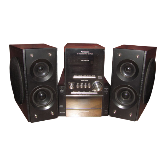
- Page 13 8. Front Panel Controls...
- Page 15 9. Disassembly and Main Component Replacement Procedures. “ATTENTION SERVICER” Some chassis components maybe have sharp edges. Be careful when diassembling and servicing. 1. This section describes procedures for checking the operation of the major printed circuit boards and replacing the main components.
- Page 16 - Disassembly of Traverse Mechanism - Main Component Replacement Procedures 1. Procedure of replacing Cassette Holder 2. Procedure of replacing Pinch Roller and Head Block (Cassette Mechanism Unit) 3. Procedure of replacing Motor, Capstan Belt A, Capstan Belt B and Winding Belt (Cassette Mechanism Unit) 4.
- Page 17 Step 3 Remove all the screws and pull up the cassette lid as the arrow shown. Step 4 Release the connectors CN307, CN308 and CN1303. Remove the cassette lid. Step 5 Release the connector CN310 and pull out the back cover as the arrow shown.
- Page 18 Step 6 Release the connectors CN504, CN305 and CN301. Step 7 Release the connectors CN606, CN602, CN505, CN500 and remove all the screws.
- Page 19 Step 8 Remove all the screws. Step 9 Release the catches and pull out the front panel as the arrow shown. Step 10 Remove all the screws and release the connector CN607A.
- Page 20 Steps 11 & 12 Remove all the screws. Step 13 Remove all the screws and pull up the cover as the arrow shown.
- Page 21 Step 14 Remove all the screws. Step 15 Reconnect all the connectors back to do the testing. 9.2. Procedure for Replacing Cassette Holder - Follow Steps 1 to 4 described in Item 9.1. Step 2 Press the lever to open the cassette cover.
- Page 22 9.3. Procedure for Replacing Pinch Roller and Head Block (Cassette Mechanism Unit) - Follow Steps 1 to 4 described in Item 9.1. - Follow Steps 1 to 3 described in Item 9.2.
- Page 24 9.4. Procedure for Replacing Motor, Capstan Belt A, Capstan Belt B, and Winding Belt (Cassette Mechanism Unit) - Follow Steps 1 to 4 described in Item 9.1. - Follow Steps 1 to 3 described in Item 9.2. - Follow Steps 2 to 4 described in Item 9.3.
- Page 26 9.5. Procedure for Replacing Parts on Mechanism PCB - Follow Steps 1 to 4 described in Item 9.1.
- Page 27 - Follow Steps 1 to 3 described in Item9.2. - Follow Steps 2 to 4 described in Item 9.3. 9.6. Replacement of CD traverse deck - Follow Steps 1 to 14 described in Item 9.1.
- Page 28 9.7. Replacement of optical pickup unit (CD mechanism) - Follow Steps 1 to 14 described in Item 9.1. - Follow Steps 1 to 2 described in Item 9.6.
- Page 32 9.8. Replacement of a traverse gear A and a traverse gear B - Follow Steps 1 to 14 described in Item 9.1. - Follow Steps 1 to 2 described in Item 9.6. - Follow Steps 1 to 12 described in Item 9.7.
- Page 33 9.9. Disassembly of CD loading unit 9.9.1. Regarding a jig "gear" - The gear is equipped to the unit to check the opening and closing of the disk tray and the hoisting of traverse unit manually at the maintenance service. (The usage of the gear is described in this disassembly procedure).
- Page 34 used. 1. Remove the gear attached to the top cover of CD loading mechanism. 2. Insert a hexagonal wrench of 2.5mm (opposite side diameter) into the gear. 9.10. Replacement of disk tray - Follow Steps 1 to 14 described in Item 9.1.
- Page 37 9.11. Replacement of the traverse mechanism - Follow Steps 1 to 7 described in Item 9.10.
- Page 38 9.12. Disassembly of CD loading section - Follow Steps 1 to 7 described in Item 9.10. - Follow Step 1 described in Item 9.11.
- Page 42 9.13. Assembly of CD loading unit - For assembly of CD loading unit, follow the reverse way of the disassembly procedure. And see following procedure as there are some points to be noticed in the assembly. 9.13.1. Notes on fixing of CD loading section 9.13.1.1.
- Page 43 9.13.1.2. Notes on fixture of a vertical drive gear and GENEVA gear 1. Fix a vertical drive gear, GENEVA gear, a vertical reduction gear, gears (2 pieces) and a relay gear. 2. The marking should be at the position as shown below figure to fix a vertical drive gear.
- Page 44 3. Set a hole as shown below to fix GENEVA gear. 9.13.1.3. Notes on fixing a vertical rack (L) 1. Fix vertical rack (L) and (R). 2. Position the concave portion of a vertical rack (L) to trapezoidal...
- Page 45 cog of a vertical rack (L) and fix. 3. Fix a timing gear plate and a timing gear, then fasten them with screws. 9.13.1.4. Notes on fixing of a change gear and a main gear 1. Fix a change lever and a change gear following 2. Then fix a level drive gear and a main gear spring, and fix a main gear following 3 and 4.
- Page 46 2. Position a convex portion of a change gear to a marking of a mechanism base and fix. 3. Position a hole of a main gear against a boss (a) of a mechanism base and fix. 4. Rotate a main gear to the arrow direction to position a hole of a main gear to a boss (b).
- Page 47 5. Draw up a select rack to the far front part. 9.13.1.5. Notes on fixing a pitch plate 1. Fix a reduction gear (2), a relay gear, a pulley gear, a tray relaying gear and a large belt (2).
- Page 48 2. Fix a level reduction gear (1), a horizontal reduction gear (2), a relay gear, a reverse gear, a speedup gear and a small belt (1). 3. Position the edge of a dividing lever (1) to the position shown in figure 1.
- Page 49 9.13.1.6. Notes on fixing a traverse mechanism 1. Fix a vertical lever. (Fit a rib into both side grooves) 2. Fit a traverse mechanism into the groove. 3. The projecting portion of a dividing lever (2) should be inserted...
- Page 50 into a concave portion of a dividing lever (1). 4. Set a loading gear at the position shown by figure 2. 5. Draw a vertical rack (R) to the arrow direction. 9.13.1.7. Notes on fixing a disk tray 1. Fix a tray drive gear and a tray drive gear shaft. / (Position the lowest rib of a tray drive gear to be level) 2.
- Page 51 3. Check the phase. A. The projecting portion of a dividing lever (2) should be inserted into a concave portion of a dividing lever (a). B. Seta loading gear at the position shown by figure 2. C. The hole A of pitch plate should be positioned at a hole of a main gear.
- Page 52 5. Fix a speedup lock. 6. Fix an open switch lever. / (Insert a boss of an open switch lever into the hole of mechanism base)
- Page 53 7. Fix a top cover. / (Fix to the arrow direction after putting into the catch) 9.14. Disassembly of traverse mechanism - Follow Steps 1 to 14 described in Item 9.1. - Follow Steps 1 to 7 described in Item 9.10. - Follow Step 1 descrbed in Item 9.11.
- Page 55 9.15. Handling of cassette tape jam - Follow Steps 1 to 3 described in Item 9.1.
- Page 56 10. Procedure for Checking Operation of Individual Parts of Cassette Mechanism Unit 10.1. Operation Check with Cassette Tape 1. Pull up the EJECT lever using a rubber band. (Cf. Fig. 6) 2. Supply DC5V to MOTOR. ( MOTOR rotates.) (Cf. Fig. 5) 3.
- Page 57 (ON: approx. 5msec) D. REV PLAY: Supply the plunger power in a normal timing at STOP mode. (ON: approx. 200msec) E. REV REW: Supply the plunger power in a flash at REV PLAY mode. (ON: approx. 50msec) F. STOP: Supply the plunger power in a flash at FF mode. (ON: approx.
- Page 58 3. Lift up the mechanism unit’s plunger/rib with the tip of a negative screwdriver, and operate the unit in the same timing as / supplying the power. (Cf. Fig. 7) / (Note) Follow Step 4 in Item 1.1. for procedure on operatingeach function. 11.
- Page 59 Block (Cassette Mechanism Unit)] under [9. Disassembly and Main Component Replacement Procedures before Operation Checks]. 3. Connect the headphone jack output jig (cf. Fig. 8) to headphone jack. 11.2.4. Head Azimuth Adjustment 1. Connect an oscilloscope. (Cf. Fig. 10) 2. Playback the azimuth adjustment portion (8kHz, -20dB) of the test tape (QZZCFM).
- Page 60 the test tape (QZZCFM). Check that the level difference when the tape is played in forward and reverse directions does not exceed 1.5dB. 5. After the adjustment, fasten screwlock to the azimuth adjusting screw. (Note) Before adjusting the head azimuth, be sure to remove the screwlock adhesive attached around the head for fine adjustments.
- Page 61 produced. (Cf. Fig. 16) Adjustment Range: 3,000 ± 90Hz (a constant speed) 11.2.6. Bias Voltage Check 1. Connect an electrical voltmeter. (Cf. Fig. 9) (Cf. Fig. 14) 2. Set the function to “TAPE” position. 3. Insert a normal blank cassette tape (QZZCRA). 4.
- Page 62 13. Schematic Diagram (All schematic diagrams may be modified at any time with the development of new technology.) Notes: Switch Switch Switch Trigger Switch S600 Rec Switch S601 Preset EQ Switch S602 Tape Eject Switch S603 Rew Switch S604 Stop/Demo Switch S605 FF Switch S606...
- Page 63 - Importance safety notice: Components identifed by mark have special characteristics important for safety. Furthermore, special parts which have purposes of fire-retardant (resistors), high-quality sound (capacitors), low-noise (resistors), etc. are used. Whenreplacing any of components, be sure to use only manufacturer’s specified parts shown in the parts list.
- Page 64 16. Troubleshooting Flowchart (CD Section Circuit)
- Page 66 17. Type Illustrations of ICs, Transistors& Diodes 18. Terminal Function of IC’s 18.1. IC701 (AN8885SBE1) Servo Amplifier...
- Page 67 Pin No. Mark Function Tracking signal input 1 Tracking signal input 2 Power supply Focus signal input terminal 1 Focus signal input terminal 2 APC amp input APC amp output RFsumming output RFIN Detector’s input CSBRT I Capacitor for OFTR connection Capacitor for HPF amp connection...
- Page 68 Mark Function BCLK N.C. LRCK N.C. SRDATA O N.C. DVDD1 Power supply input (for digital circuit) DVSS1 GND (for digital circuit) Digital audio interface signal output (Latches data at first transition) MCLK Microprocessor command clock signal input MDATA Microprocessor command data signal input Microprocessor command load signal...
- Page 69 SQCK)
- Page 70 Mark Function /RST Reset signal input SMCK 1/2-diveded clock signal of crystal osscillating at MSEL = “H” (fSMCK = 8.4672 MHz) 1/4-divided clock signal of crystal oscillating at MSEL = “L” (fSMCK = 4.2336MHz) CSEL Frequency Selection Terminal H = 33.8688 MHz ;...
- Page 71 Mark Function TRCRS Track cross signal input /RFDET RF detection signal input ("L" : detection) Dropout signal input ("H" : Dropout) LDON Laser on signal output ("H" : ON) PLLF2 N.C. DSLF2 Tracking Offset alignment output/DSL Balance Output (DA Output) WVEL N.C.
- Page 72 Mark Function X1 IN Crystal oscillating circuit input (f = 16.9344MHz) X2 OUT Crystal oscillating circuit input (f = 16.9344 MHz) Power supply input (for oscillating circuit) BYTCK Byte clock output /CLDCK - Sub-code frame clock signal output (fCLDCK = 7.35 kHz during normal playback) FCLK...
- Page 73 Mark Function RSEL RF signal polarity assignment input (at "H" level, RSEL="H", at "L" level, RESL= "L") IOVOD 5V supply input PSEL Test terminal (connected to Gnd) MSEL SMCK oscillating frequency designation input (“L” :4.2336 MHz, “H”: 8.4672 MHz) SSEL SUBQ output mode select (“H”:Q-code buffer mode)
- Page 74 Mark Function Motor driver (4) reverse- action output Motor driver (4) forward- action output N.C. PGND2 - Ground connection (2) for driver PVCC2 I Power supply (2) for driver N.C. Power supply terminal VREF Reference voltage input Motor driver (4) input Motor driver (3) input RSTIN Reset terminal...
- Page 75 1,000(ohms). - The marking (RTL) indicates that the Retention Time is limited for this item. After the discontinuation of this assembly in production, the item will continue to be available for a specific period of time. The retention period of availabilityis dependant on the type of assembly, and in accordance with the lows govening part and product retention.
- Page 76 19.1.2. Deck Mechanism Parts List...
- Page 77 Ref. No. Part No. Part Name & Description Remarks CASSETTE DECK RED0071 R/P HEAD BLOCK UNIT RDG0300 REEL BASE GEAR RDG0301 WINDING RELAY GEAR RDK0026 MAIN GEAR RDV0033-4 WINDING BELT RDV0034-1 CAPSTAN BELT A RMB0312 TRIGGER LEVER SPRING RMB0400 REEL SPRING RMB0403 HEAB PANEL SPRING RMB0404...
- Page 81 19.2.2. CD Loading Mechanism Parts List...
- Page 82 Ref. No. Part No. Part Name & Description Remarks TRAVERSE DECK RAE0155A-V TRV UNIT WITHOUT SERVO PCB RDG0455 TRV GEAR (A) RDG0456 TRV GEAR (B) RDG0519 MAIN GEAR RDG0520 SPEED UP GEAR RDG0521 REVERSE GEAR RDG0522 GENEVA GEAR RDG0523 HOR RELAY GEAR RDG0525 CROWN GEAR RDG0526...
- Page 83 Ref. No. Part No. Part Name & Description Remarks RMM0242 TRV.SLIDE PLATE [R] RMM0243 SELECT RACK RMM0244 SELECT GUIDE RMQ1051 PITCH PLATE RMQ1052 UD BASE RMQ1056 TRAY GUIDE [L] RMQ1057 TRAY GUIDE [R] RMQ1058 GEAR HOLDER RMQ1059 TOP COVER RMQ1060 CLAMP GUIDE RMQ1061 TG.PLATE...
- Page 85 19.3.2. Cabinet& CD Loading Mechanism Parts List...
- Page 86 Ref. No. Part No. Part Name & Description Remarks CABINET AND CHASSIS REE1172 3P BLUE LED REEX0165 14P FFC REEX0166 14P FFC WIRE REEX0167 19P CD FFC REEX0168 30P FFC REM0094 COLLING FAN RGK1512-S VOLUME RING RGK1513-S REC BUTTON RING RGKX0128A-S FRONT ORNAMENT RGK1515-S1...
- Page 87 Ref. No. Part No. Part Name & Description Remarks RDG0357 DAMPER GEAR RGL0591-Q REC LIGHTING TIP XTWS3+8T SCREW 19.4. Components Parts List Ref. No. Part No. Part Name & Description Remarks P.C.B. REP2807E CD SERVO P.C.B. REP3340A CD LOADING P.C.B. REPX0289B DECK P.C.B.
- Page 88 Ref. No. Part No. Part Name & Description Remarks Q514 2SD0592ARA TRANSISTOR Q515 KTC3199GRTA TRANSISTOR Q516 KTC3199GRTA TRANSISTOR Q517 KTC32030YTA TRANSISTOR Q519 B1AAGC000006 TRANSISTOR Q575 B1AAGC000006 TRANSISTOR Q577 2SC3940ARA TRANSISTOR Q578 KRC102MTA TRANSISTOR Q579 2SB621ARSTA TRANSISTOR Q607 KRC103STA TRANSISTOR Q608 KTC3875GRTA TRANSISTOR Q609...
- Page 89 Ref. No. Part No. Part Name & Description Remarks Q1317 B1ABGC000005 TRANSISTOR DIODES D101 UDZSTE175R1B DIODE D301 RL1N4003S-P DIODE D302 RL1N4003S-P DIODE D500 KBL402G DIODE D505 B0AACK000004 DIODE D508 MAZ4150NLF DIODE D515 B0BA9R600002 DIODE D517 B0BA5R600016 DIODE D518 B0AACK000004 DIODE D520 B0BA9R600002 DIODE...
- Page 90 Ref. No. Part No. Part Name & Description Remarks D643 RB501V-40 DIODE D644 B0ACCK000005 DIODE D645 B0ACCK000005 DIODE D700 B0AACK000004 DIODE D701 B0AACK000004 DIODE D702 B0AACK000004 DIODE D703 B0AACK000004 DIODE D704 B0AACK000004 DIODE D705 B0AACK000004 DIODE D706 B0AACK000004 DIODE D707 B0AACK000004 DIODE D708...
- Page 91 Ref. No. Part No. Part Name & Description Remarks S975 RSH1A019-2U SW LEAF CONNECTORS K1MN14B00066 14P FFC CONN. (SIDE) CN301 RJU100W13 13P CONNECTOR CN305 RJS2A8030 P1 FFC CONNECTOR ST CN306 K1MN14C00004 14P FFC CONNECTOR CN307 K1MP09A00002 TO MAIN MOLEX CN308 K1KA02B00115 LASER CONNECTOR CN310...
- Page 92 Ref. No. Part No. Part Name & Description Remarks COMPONENT COMBINATION Z101 RLA2Z007-T COIL Z102 RLI2Z021M-T AM IF BLOCK Z120 ENV17290G1Y FM TUNER PACK Z501 ERZV10V511CS ZENER Z602 B3RAB0000016 INFRARED RAYS Z971 RGSD12A1445T RADA RESISTOR SP600 RMB0712 EARTH SPRING CERAMIC FILTERS CF201 J0B1075A0086 CERAMIC CAPACITOR...
- Page 93 Ref. No. Part No. Part Name & Description Remarks H605A RMR0316 7P WIRE HOLDER H605B RMR0316 7P WIRE HOLDER H607A RMR0321 WIRE HOLDER FOR W902 H634 RMN0655 LED HOLDER H1304 RMR0318 9P WIRE HOLDER JACKS JK101 RJH8304N JK ANTENNA JK300 GP1F32T JK OPT TERMINAL JK301...
- Page 94 Ref. No. Part No. Part Name & Description Remarks R120 ERJ3GEYJ473V 47K 1/16W R121 ERJ3GEYJ223V 22K 1/16W R122 ERJ3GEYJ272V 2.7K 1/16W R123 ERJ3GEYJ683V 68K 1/16W R124 ERJ3GEYJ330V 33 1/16W R125 ERJ3GEYJ471V 470 1/16W R126 ERJ3GEYJ102V 1K 1/16W R127 ERJ3GEYJ471V 470 1/16W R128 ERJ3GEYJ820V 82 1/16W...
- Page 95 Ref. No. Part No. Part Name & Description Remarks R347 ERJ3GEYJ101V 100 1/16W R348 ERJ3GEYJ121V 120 1/16W R391 ERJ3GEYJ102V 1K 1/16W R393 ERJ3GEYJ102V 1K 1/16W R394 ERJ3GEYJ102V 1K 1/16W R395 ERJ3GEYJ104V 100K 1/16W R401 ERJ3GEYJ103V 10K 1/16W R402 ERJ3GEYJ182V 1.8K 1/16W R403 ERJ3GEYJ822V 8.2K 1/16W...
- Page 96 R540 ERDS2TJ153T 15K 1/4W...
- Page 97 Ref. No. Part No. Part Name & Description Remarks R541 ERDS2TJ153T 15K 1/4W R542 ERDS2TJ562T 5.6K 1/4W R543 ERDS2TJ562T 5.6K 1/4W R544 ERDS2TJ472T 4.7K 1/4W R545 ERDS2TJ472T 4.7K 1/4W R546 ERDS2TJ223T 22K 1/4W R547 ERDS2TJ683T 68K 1/4W R548 ERDS2TJ184T 180K 1/4W R549 ERDS1FVJ2R2T 2.2 1/2W...
- Page 98 R614 ERJ3GEYJ222V 2.2K 1/16W...
- Page 99 Ref. No. Part No. Part Name & Description Remarks R615 ERJ3GEYJ182V 1.8K 1/16W R616 ERJ3GEYJ122V 1.2K 1/16W R617 ERJ3GEYJ102V 1K 1/16W R618 ERJ3GEYJ102V 1K 1/16W R619 ERJ3GEYJ103V 10K 1/16W R620 ERJ3GEYJ103V 10K 1/16W R621 ERJ3GEYJ101V 100 1/16W R622 ERJ3GEYJ101V 100 1/16W R623 ERJ3GEYJ223V 22K 1/16W...
- Page 100 Ref. No. Part No. Part Name & Description Remarks R673 ERJ3GEYJ334V 330K 1/16W R674 ERJ3GEYJ106V 10M 1/16W R675 ERJ3GEYJ472V 4.7K 1/16W R676 ERJ3GEYJ472V 4.7K 1/16W R677 ERJ3GEY0R00V 0 1/16W R678 ERJ3GEYJ101V 100 1/16W R679 ERJ3GEYJ103V 10K 1/16W R680 ERJ3GEYJ102V 1K 1/16W R681 ERJ3GEYJ103V 10K 1/16W...
- Page 101 R716 ERDS2TJ102T 1K 1/4W [M]EG E...
- Page 102 Ref. No. Part No. Part Name & Description Remarks R717 ERJ3GEYJ102V 1K 1/16W R718 ERJ3GEYJ102V 1K 1/16W R720 ERDS2TJ563T 56K 1/4W R721 ERDS2TJ563T 56K 1/4W R721 ERJ3GEYJ101V 100 1/16W R722 ERDS2TJ104T 100K 1/4W R723 ERDS2TJ102T 1K 1/4W R723 ERJ3GEYJ103V 10K 1/16W R724 ERDS2TJ104T 100K 1/4W...
- Page 103 Ref. No. Part No. Part Name & Description Remarks R755 ERDS2TJ220T 22 1/4W R756 ERDS2TJ220T 22 1/4W R757 ERDS2TJ220T 22 1/4W R758 ERDS2TJ222T 2.2K 1/4W R759 ERDS2TJ472T 4.7K 1/4W R760 ERDS2TJ223T 22K 1/4W R760 ERJ3GEYJ221V 220 1/16W R761 ERDS2TJ223T 22K 1/4W R761 ERJ3GEYJ472V 4.7K 1/16W...
- Page 104 Ref. No. Part No. Part Name & Description Remarks R925 ERJ3GEYJ223V 22K 1/16W R926 ERJ3GEY0R00V 0 1/16W R927 ERJ3GEY0R00V 0 1/16W R972 ERDS2TJ821T 820 1/4W R973 ERDS2TJ393T 39K 1/4W R1101 ERJ3GEYJ270V 27 1/16W R1102 ERJ3GEYJ152V 1.5K 1/16W R1103 ERJ3GEYJ183V 18K 1/16W R1104 ERJ3GEYJ103V 10K 1/16W...
- Page 105 R1344 ERJ3GEYJ273V 27K 1/16W...
- Page 106 Ref. No. Part No. Part Name & Description Remarks R1345 ERJ3GEYJ102V 1K 1/16W R1371 ERJ3GEYJ223V 22K 1/16W R1374 ERJ3GEYJ471V 470 1/16W CAPACITORS F1D1E103A001 0.01 25V ECA1CAK101XB 100 16V F1D1E103A001 0.01 25V ECA1CAK101XB 100 16V C101 ECUV1E103KBV 0.01 25V C102 ECA1CAK101XB 100 16V C103 ECUV1E103KBV...
- Page 107 Ref. No. Part No. Part Name & Description Remarks C203 ECA1HAK4R7XB 4.7 50V C204 ECJ1VB1H102K 1000P 50V C205 ECA1HAK2R2XB 2.2 50V C206 ECUV1H221KBV 220P 50V C207 ECA1CAK100XB 10 16V C208 ECA1HAK2R2XB 2.2 50V C209 ECA1HAK2R2XB 2.2 50V C210 ECUV1H471KBV 470P 50V C211 ECQV1H104JZ3 0.1 50V...
- Page 108 Ref. No. Part No. Part Name & Description Remarks C416 ECUV1H101JCV 100P 50V C417 ECJ1VB1H102K 1000P 50V C418 ECUV1E473KBV 0.047 25V C419 ECUV1E473KBV 0.047 25V C425 F1D1H102A012 1000P 50V C500 F1D1H821A012 820P 50V C501 F1D1H821A012 820P 50V C502 F1D1H821A012 820P 50V C503 F1D1H821A012 820P 50V...
- Page 109 Ref. No. Part No. Part Name & Description Remarks C621 ECUV1H103KBV 0.01 50V C622 ECA1CAK220XB 22 16V C623 ECUV1H561KBV 560P 50V C624 ECUV1H561KBV 560P 50V C625 ECUV1H561KBV 560P 50V C626 ECUV1H561KBV 560P 50V C627 ECUV1H101JCV 100P 50V C628 ECUV1H101JCV 100P 50V C632 ECUV1C223KBV 0.022 16V...
- Page 110 Ref. No. Part No. Part Name & Description Remarks C710 F1D1H102A012 1000P 50V C711 ECA1CAK100XB 10 16V C711 ECUV1C104KBV 0.1 16V C712 ECUV1C104KBV 0.1 16V C712 F1D1H473A012 0.047 50V C713 ECA1HAKR68XB 0.68 50V C713 ECUV1C104KBV 0.1 16V C714 ECEA0JKA101I 100 6.3V C714 ECQV1H274JZ3 0.27 50V...
- Page 111 Ref. No. Part No. Part Name & Description Remarks C743 ECBT1H103KB5 0.01 50V C743 ECUV1E104ZFV 0.1 25V C744 ECBT1H103KB5 0.01 50V C744 ECUV1H562KBV 5600P 50V C745 ECUV1E104ZFV 0.1 25V C745 F1D1H101A012 100P 50V C746 F1D1H101A012 100P 50V C747 ECUV1H181JCV 180P 50V C747 F1D1H101A012 100P 50V...
- Page 112 Ref. No. Part No. Part Name & Description Remarks C1307 ECA1AAK221XQ 220 10V C1308 ECA1CAK220XB 22 16V C1310 ECA1HAK0R1XB 0.1 50V C1311 ECA1CAK470XB 47 16V C1312 ECUV1H332KBV 3300P 50V C1314 ECUV1H222KBV 2200P 50V C1315 ECUV1H222KBV 2200P 50V C1316 ECJ1VB1H102K 1000P 50V C1317 ECJ1VB1H102K 1000P 50V...
- Page 113 Ref. No. Part No. Part Name & Description Remarks PACKING MATERIALS RPGX0948 PACKING CASE RPNX0145 POLYFOAM RPHV0001 MIRAMAT SHEET ACCESSORIES EUR648265 REMOTE CONTROL A1-1 UR64EC2337A R/C BATTERY COVER RJA0019-2K AC CORD (SF) [M]EG E VJA0733 AC CORD (SF) [M]EB RQT6398-B O/I BOOK (En) [M]EB E RQT6399-E...
- Page 114 / Printed in Singapore / M020600001FLE/K/E/J/A/S/N...
- Page 115 SCHEMATIC DIAGRAM-3 : AUX SIGNAL LINE : PLAYBACK SIGNAL LINE MAIN CIRCUIT : +B SIGNAL LINE : AM/FM SIGNAL LINE : RECORD SIGNAL LINE LINE OUT R201 C201 R202 C225 470P 1.8K 1000P C401 R402 L392 470P 1.8K 100µH R401 C425 JK303 1000P...
- Page 116 SCHEMATIC DIAGRAM-4 : AUX SIGNAL LINE : PLAYBACK SIGNAL LINE : MAIN SIGNAL LINE MAIN CIRCUIT : +B SIGNAL LINE : AM/FM SIGNAL LINE : RECORD SIGNAL LINE : CD SIGNAL LINE S602 TAPE EJECT DECK EJECT CIRCUIT W308 CN308/WH308 C416 C400 R213...
- Page 117 SCHEMATIC DIAGRAM-7 PANEL CIRCUIT : +B SIGNAL LINE : MAIN SIGNAL LINE FL600 A2BD00000052 FL DISPLAY 1 2 3 4 5 6 7 8 9 10 11 12 13 14 15 16 17 18 19 20 21 22 23 24 25 26 27 28 29 30 31 32 33 34 35 36 37 38 39 40 41 42 43 44 C601 C602 35V22...
- Page 118 SCHEMATIC DIAGRAM-8 DECK CIRCUIT (CN1303) ON : MAIN SIGNAL LINE SCHEMATIC DIAGRAM-10 PANEL CIRCUIT : +B SIGNAL LINE : CD SIGNAL LINE H600/W600 Q613,615 R687 R688 D632 L605 KRA119STA UDZSTE174R7B 100µH LED DRIVE MOTOR Q904 Q905 C646 KRC101STA 50V3.3 KRC101STA MOTOR SWITCH PLUNGER SWITCH REC_LED...
- Page 119 SCHEMATIC DIAGRAM-11 power pcb (E/EG) power pcb (EB) POWER CIRCUIT : +B SIGNAL LINE : MAIN SIGNAL LINE Q700 Q702 B1AACF000063 B1AACF000063 SWITCH R704 SWITCH Q701 KTA12710YTA R778 SWITCH Q701 C700 R702 R707 D708 6.3V100 R776 5.6K MA2C16500E Q720 KTC3199GRTA Q700 R774 C738...
- Page 120 SCHEMATIC DIAGRAM-12 : -B SIGNAL LINE POWER CIRCUIT : +B SIGNAL LINE : MAIN SIGNAL LINE Q703 B1AACF000063 IC500 SWITCH IC500 RSN314H41A-P Q703 POWER AMP D707 C515 B0AACK000004 0.01 R709 C702 C503 820K 50V2.2 R514 820P HI_R C501 R506 C509 820P LO_L R761...
- Page 121 SCHEMATIC DIAGRAM-13 ac transformer pcb (EB) ac transformer pcb (E/EG) : -B SIGNAL LINE AC TRANSFORMER CIRCUIT : +B SIGNAL LINE D581 D578 RL1N4003S-P R580 R581 R585 RL1N4003S-P C585 D585 D579 25V100 RL1N4003S-P RL1N4003S-P CN507A R583 Q577 Q577 C584 C578 2SC3940ARA 16V1000 C580...
- Page 122 SCHEMATIC DIAGRAM-5 : +B SIGNAL LINE : AM SIGNAL LINE MAIN (TUNER) CIRCUIT : FM OSC SIGNAL LINE : AM OSC SIGNAL LINE : FM SIGNAL LINE Z120 ENV17290G1Y C103 0.01 R107 2SK238 2SC2620 CF201 R106 J0B1075A0086 HVM27 HVM27 470K FM EXT ANT C104 1000P...
- Page 123 SCHEMATIC DIAGRAM-6 : AM SIGNAL LINE : AM OSC SIGNAL LINE MAIN (TUNER) CIRCUIT : +B SIGNAL LINE : FM SIGNAL LINE : FM/AM SIGNAL LINE R104 Q110 R109 2SC3311ARTA CF202 C105 R108 J0B1075A0077 SWITCH +7.5V 1000P 470K R139 Q110 DET_OUT Q102 R121...
- Page 124 POWER P.C.B. ( REPX0279K...EB Q720 C740 D526 J771 R778 C742 R764 C736 D527 C741 R758 D517 CN500 C709 R767 R728 R771 R753 IC501 D701 C743 C730 R759 R773 Q514 R729 C747 C749 C731 Q721 R727 C745 R756 R721 R755 J750 R775 Q718 C728...
- Page 125 AC TRANSFORMER P.C.B. ( REPX0279K...EB L503 JK501 CN507B RL501 J517 CN507A Z501 J518 J519 J512 J513 J514 J520 FP502 D585 C588 C584 R576 D592 D593 D582 D581 C587 D586 R581 R580 C580 Q577 D505 C581 C585 C586 J521 J510 CN505 J516...
- Page 126 POWER P.C.B. ( REPX0279L...E/EG Q720 C740 D526 J771 R778 C742 R764 C736 D527 C741 R758 D517 CN500 C709 R767 R728 R771 R753 IC501 D701 C743 C730 R759 R773 Q514 R729 C747 C749 C731 Q721 R727 C745 R756 R721 R755 J750 R775 Q718 C728...
- Page 127 AC TRANSFORMER P.C.B. ( REPX0279L...E/EG L503 JK501 CN507B RL501 J517 CN507A Z501 J518 J519 J512 J513 J514 J520 FP502 D585 C588 C584 R576 D592 D593 D582 D581 C587 D586 R581 R580 C580 Q577 D505 C581 C585 C586 J521 J510 CN505 J516...
- Page 128 MN662790RSC (80p) BA5948FPE2 (28P) AN8885SBE1 (28p) C0AABB000117 CNB13030R2AU C2BBGF000357 (100p) AN7326K (26p) LA1833NMNTLM (24p) LC72131MDTRM (20p) C1BB00000617 (30p) C3EBCG000008 (16p) C1BB00000527 (16p) KRA102MTA RSN314H41A-P C0GAG0000007 C1AA00000612 B1AAGC000006 KTC3199GRTA KRC102MTA KRA110MTA DTA114EKA146 KTC3875GRTA KTA1046 KRC119STA 2SD0592ARA DTA143XKA146 KRC101STA KTC2026 2SD09650RA DTC114EKA146 KRC102STA KTA12710YTA DTC143XKA146...
- Page 129 DECK P.C.B (REPX0289B) IC1001 C1101 J1021 C1323 C1321 C1201 J1061 R1101 C1103 J1019 C1322 C1203 C1121 C1104 C1204 C1325 J1017 R1302 C1318 C1303 R1102 C1223 C1122 C1108 R1333 C1106 C1302 J1306 IC1000 R1330 C1123 C1109 R1303 C1301 R1334 C1319 R1336 C1316 C1308 C1305...
- Page 130 TACT SWITCH P.C.B. ( REPX0278J Z602 S605 S603 S604 S600 S601 R604 R602 STOP/DEMO PRESET_EQ C647 R603 C648 R693 Q614 VR600 D638 S606 S609 S607 S608 S619 D633 3 2 1 C627 PLAY/PAUSE TUNER/BAND TAPE PLAY S610 SSEQ S618 R606 R607 R608 R609...
- Page 131 CD LOADING P.C.B (REP3340A)
- Page 132 tuner circuit main circuit MAIN/TUNER P.C.B. ( REPX0278J R301 R302 C130 C134 L392 J208 X103 J107 C395 J206 R137 R136 R393 R135 R134 R133 R151 R129 R117 C124 R391 R138 R127 J105 R132 C394 C122 R152 X391 R122 C397 C113 C121 C141 J212...
- Page 133 POWER-ON P.C.B. REPX0278J R637 C130 R111 C134 R113 X103 R114 CN609B J107 R136 C110 R135 R134 R133 R151 J122 R129 R117 J102 C124 R138 D634 R127 J105 R105 R132 R152 C113 C141 R110 C103 C129 J134 C142 C108 J118 R123 C139 R106 R107...
- Page 134 PANEL P.C.B. ( REPX0278J J646 J644 H605A CN608 R708 R903 J638 J639 J691 J674 C651 J693 J690 R919 J673 C653 J676 J672 D641 C652 R918 J681 R697 J662 J685 R699 R927 Q903 C656 D644 J633 CN606 R644 J660 R639 D645 J659 Q607 D630...
- Page 135 CD SERVO P.C.B (REP2807E) (RF) TJ701 X701 C727 TJ701 TP19 C725 C717 R714 C726 TP16 C721 C744 C728 C716 R709 C702 TP17 TP26 C722 TP24 TP25 C724 R712 TP18 TP35 TP27 C723 TP13 R721 IC701 TP14 J723 C730 C732 TP11 C711 J726 J702...
- Page 136 IC701 CD OPTICAL PICKUP AN8885SBE1 SERVO AMP SEMICONDUCTOR LASER RFEQ1 Q701 OFTR LASER POWER DRIVE TENV RFEQ2 /RFDET /RFDET DET. VREF FEOUT SUBTRACTER PHOTO DETECTOR VREF TEOUT SUBTRACTER VREF BAND [CH3] LEVEL FOCUS COIL SHIFT RSTIN [CH4] TRACKING COIL LEVEL SHIFT TRV+ M701...
- Page 137 TO MAIN BLOCK IC702 MN662790RSC SERVO PROCESSOR /DIGITAL SIGNAL PROCESSOR DIGITAL FILTER /D/A CONVERTER CLVS OUTR BLKCK /CLDCK SBCK SUBC OUTL CD SIGNAL DEMPH SQCK ST/DO FLAG SUBQ SUBQ IPFLAG DIGITAL AUDIO INTERFACE PLLF DIGITAL AUDIO INTERFACE PLLF2 LRCK DSLF2 DSLF SRDATA INTERPOLATION/...
- Page 138 AM ANT FM ANT CF202 Z120 CF201 Q101, Q102 Z101 SWITCHING, MIXER FM IF AMP (FM) RF AMP BUFFER COIL COIL (FM) Q110 SWITCH DECODER RM AMP PHASE PILOT BUFFER CANCEL LEVEL S-CURVE STEREO SWITCH AM/FM BUFFER COMP TUNING DRIVE PILOT X102 IC101...
- Page 139 FILTER FILTER CD SIGNAL TEST LVREF CONTROL CIRCUIT JK303 CONTROL CIRCUIT INTERFACE CONTROL CIRCUIT RVREF VREF IC301 C1BB00000617 ELECTRONIC VOLUME CONTROL & TONE CONTROL MPXIN IC302 Q902 FLOUT C1BB00000527 X391 STAT STATUS SWITCH XOUT Q901 SUBQ SUBQ SWITCH Q903 BLKCK IC11 IC21 BLKCLK...
- Page 140 Q1101 (Q1201 ) MUTING SWITCH FILTER R/P HEAD (Lch) FILTER IC1001 AN7326K P/B REC AMP 22(1) 21(2) 20(3) 19(4) 15(8) 16(7) RIPPLE REJECTION LOGIC SWITCH REC AMP (L) MUTE IC1000 C1AA00000612 ANALOG SWITCH Q1302 DECK MUTING CONT. Q1304 SWITCH (REC:H) Q1317 Q1303 BEAT PROOF...
- Page 141 IC501 Q1315 C0AABB000117 DUAL_OP_AMP SWITCH Q721(Q720) D951 Q1314, Q1316 SWITCH (MOTOR HP_L(R) SUPPLY) JK600 HEADPHONE Q503 Q507 D541 D518 MUTING MUTING MUTE_A SWITCH SWITCH Q905 Q904 SYNC D528 PLUNGER MOTOR SWITCH SWITCH Q510 MUTING SWITCH HP_L(R) Q704 MUTE_A MUTING CONTROL MUTEH KEY SW Q700~Q703...
- Page 142 SIGNAL LINES : MAIN SIGNAL LINE : CD SIGNAL LINE : AM SIGNAL LINE : PLAYBACK SIGNAL LINE : FM OSC SIGNAL LINE : AM OSC SIGNAL LINE : FM & AM SIGNALS LINE : RECORD SIGNAL LINE : FM SIGNAL LINE : CD-DA (AUDIO/VIDEO) SIGNAL LINE : AUX SIGNAL LINE ( ) Indicates the Pin No.
- Page 143 SCHEMATIC DIAGRAM -1 CD SERVO CIRCUIT : +B SIGNAL LINE : CD SIGNAL LINE R701 OPTICAL PICKUP CIRCUIT C701 Q701 6.3V33 3.2V 2SA1037AKSTX C703 LASER DIODE Q701 6.3V100 LASER POWER DRIVE CN701 2.7V ((2.3V)) 0.9V ((2V)) C704 R754 LD GND NBOUT C707 C714...
- Page 144 SCHEMATIC DIAGRAM - 2 CD SERVO CIRCUIT : +B SIGNAL LINE : CD SIGNAL LINE D750 MAZ80560ML R717 C727 50V1 C725 1000P R721 C726 1000P R718 C728 50V1 R761 C731 4.7K 6.3V220 CN702 Lch OUT C754 C730 C733 C732 470P A.GND 6.3V220 Rch OUT...
- Page 145 SCHEMATIC DIAGRAM-9 : PLAYBACK SIGNAL LINE DECK CIRCUIT : +B SIGNAL LINE : REC SIGNAL LINE C1105 470P R1103 C1122 C1102 0.01 470P R1101 R1104 C1104 C1303 C1307 0.027 0.033 10V220 C1101 50V1 C1121 C1107 1000P 1500P PBLIN Nor/Cro L NF GAIN Lout L EQ...
- Page 146 SCHEMATIC DIAGRAM-10 : PLAYBACK SIGNAL LINE DECK CIRCUIT : +B SIGNAL LINE : REC SIGNAL LINE R1307 Q1101, 1201 B1ABGC000005 MUTING SWITCH R1109 R1105 2.2K R1107 Q1101 R1106 100K C1123 270P R1308 R1205 R1209 2.2K R1207 Q1201 R1206 100K R1309 R1313 C1310 C1109...
- Page 147 SCHEMATIC DIAGRAM-14 CD LOADING CIRCUIT : +B SIGNAL LINE IC11 C0GAG0000007 UP/DOWN MOTOR DRIVE 0.01 16V100 RM11 UP/DOWN MOTOR BOTTOM OPEN B3NAA0000068 SENSOR STOCK PLAY MAIN CIRCUIT (CN306) ON SCHMEATIC DIAGRAM-3 IC21 C0GAG0000007 LOADING MOTOR DRIVE 0.01 16V100 RM21 LOADING MOTOR...