
Related Manuals for Motorola MVME297-002


Summary of Contents for Motorola MVME297-002
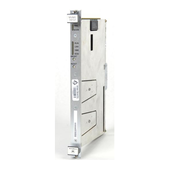
- Page 1 (217) 352-9330 | Click HERE Find the Emerson / Motorola MVME197LE at our website:...
- Page 2 MVME197DP and MVME197SP Single Board Computers User’s Manual (MVME197/D1)
- Page 3 Motorola, Inc. assumes no liability resulting from any omissions in this document, or from the use of the information obtained therein. Motorola reserves the right to revise this document and to make changes from time to time in the content hereof without obligation of Motorola to notify any person of such revision or changes.
- Page 4 Preface This document provides general information, hardware preparation and installation instructions, operating instructions, and a functional description for the MVME197DP and MVME197SP versions of the MVME197 series of Single Board Computers. This document is intended for anyone who wants to design OEM systems, supply additional capability to an existing compatible system, or work in a lab environment for experimental purposes.
- Page 5 Data and address sizes are defined as follows: A byte is eight bits, numbered 0 through 7, with bit 0 being the least significant. A two-byte is 16 bits, numbered 0 through 15, with bit 0 being the least significant. For the MVME197series and other RISC modules, this is called a half-word.
- Page 6 2. Although not shown in the above list, each Motorola Computer Group manual publication number is suffixed with characters which represent the revision level of the document, such as “/D2” (the second revision of a manual);...
- Page 7 Intel i82596 Ethernet Controller User’s Manual Cirrus Logic CD2401 Serial Controller User’s Manual SGS-Thompson MK48T08 NVRAM/TOD Clock Data Sheet The following non-Motorola publications may also be of interest and may be obtained from the sources indicated. The VMEbus Specification is contained in ANSI/IEEE Standard 1014-1987.
- Page 8 The computer programs stored in the Read Only Memory of this device contain material copyrighted by Motorola Inc., first published 1991, and may be used only under license such as the License for Computer Programs (Article 14) contained in Motorola’s Terms and Conditions of Sale, Rev. 1/79.
- Page 9 DO NOT SUBSTITUTE PARTS OR MODIFY EQUIPMENT. Because of the danger of introducing additional hazards, do not install substitute parts or perform any unauthorized modification of the equipment. Contact your local Motorola representative for service and repair to ensure that safety features are maintained.
-
Page 10: Table Of Contents
Contents CHAPTER 1 GENERAL INFORMATION Introduction ........................ 1-1 General Description ....................1-1 Features........................1-2 Specifications ......................1-3 Cooling Requirements..................1-4 FCC Compliance ....................1-5 Equipment Required....................1-5 Support Information ....................1-6 CHAPTER 2 HARDWARE PREPARATION AND INSTALLATION Introduction ........................ 2-1 Unpacking Instructions ..................... - Page 11 Processor Bus Memory Map ................3-2 Detailed I/O Memory Maps...............3-5 BBRAM, TOD Clock Memory Map ............3-18 VMEbus Memory Map ..................3-20 VMEbus Accesses to the Local Peripheral Bus ........3-20 VMEbus Short I/O Memory Map............3-20 Software Initialization....................3-20 Multi-MPU Programming Considerations ............3-21 Local Reset Operation..................3-21 CHAPTER 4 FUNCTIONAL DESCRIPTION Introduction .........................4-1...
- Page 12 List of Figures Figure 2-1. MVME197DP/SP Switches, Connectors, and LED Indicators Location Diagram........... 2-2 Figure 4-1. MVME197SP Block Diagram ..............4-2 Figure 4-2. MVME197DP Block Diagram ............... 4-3 Figure A-1. Middle-of-the-Road EIA-232-D Configuration........ A-5 Figure A-2. Minimum EIA-232-D Connection............A-6...
- Page 14 List of Tables Table 1-1. MVME197DP/SP Specifications ............1-4 Table 3-1. Processor Bus Memory Map ..............3-3 Table 3-2. Local Devices Memory Map ..............3-4 Table 3-3. BusSwitch Register Memory Map ............3-6 Table 3-4. ECDM CSR Register Memory Map ............3-7 Table 3-5.
-
Page 16: General Information
GENERAL INFORMATION Introduction This user’s manual provides general information, preparation for use and installation instructions, operating instructions, and a functional description for the MVME197DP and MVME197SP versions of the MVME197 series of single board computers, hereafter referred to as the MVME197, unless separately specified. -
Page 17: Features
General Information For the MVME197 series, the term Local Bus, as used in other MVME1xx Single Board Computers, is referred to as the Local Peripheral Bus. The BusSwitch ASIC provides an interface between the processor bus (MC88110/410 bus) and the local peripheral bus (MC68040 compatible bus). Refer to the board specific MVME197 block diagram. -
Page 18: Specifications
Specifications Dual MC88110 RISC Microprocessors, each with one MC88410 Cache Controller (MVME197DP module series only) 256 kilobytes of external cache per processor, controlled by the MC88410 128 or 256 megabytes of 64-bit Dynamic Random Access Memory (DRAM) with Error Checking and Correction (ECC) 4 megabytes of Flash memory Six status LEDs (FAIL, RUN, SCON, LAN, SCSI, and VME) 8 kilobytes of Static Random Access Memory (SRAM) and Time of Day... -
Page 19: Cooling Requirements
Cooling Requirements The Motorola MVME197 VMEmodule is specified, designed, and tested to operate reliably with an incoming air temperature range from 0˚ to 55˚ C (32˚ to 131˚ F) with forced air cooling at a velocity typically achievable by using a 100 CFM axial fan. -
Page 20: Fcc Compliance
Equipment Required a high power density system configuration. An assembly of three axial fans, rated at 100 CFM per fan, is placed directly under the VME card cage. The incoming air temperature is measured between the fan assembly and the card cage, where the incoming airstream first encounters the module under test. -
Page 21: Support Information
Detailed support information such as connector signal descriptions, the module parts list, and the schematic diagram for the MVME197DP/SP is contained in the SIMVME197 Single Board Computer Support Information manual. This manual may be obtained free of charge by contacting your local Motorola sales office. User’s Manual... -
Page 22: Hardware Preparation And Installation
HARDWARE PREPARATION AND INSTALLATION Introduction This chapter provides unpacking instructions, hardware preparation, and installation instructions for the MVME197DP/SP versions of the MVME197 series of single board computers. The MVME712X transition module hardware preparation is provided in separate manuals, refer to the Related Documentation section of this guide. - Page 23 VMEbus CONNECTOR P1 VMEbus CONNECTOR P2 1A17 2A17 3A17 CONFIGURATION SWITCH S6 SERIAL PORT 4 CLOCK SELECT 1E17 2E17 3E17 MEZZANINE CONNECTOR J1 1 2 3 4 5 6 7 8 9 CONFIGURATION SWITCH S1 GENERAL PURPOSE/SCON ABORT RESET SWITCH SWITCH MVME197 Figure 2-1.
-
Page 24: Configuration Switches
Hardware Preparation Configuration Switches The location of the switches, connectors, and LED indicators on the MVME197DP/SP is illustrated in Figure 2-1. The MVME197DP/SP has been factory tested and is shipped with factory switch settings that are described in the following sections. The MVME197DP/SP operates with its required and factory-installed Debug Monitor, MVME197Bug (197Bug), with these factory switch setting. - Page 25 Hardware Preparation and Installation Configuration Switch S1: General Purpose Functions (S1-1 to S1-8) The eight General Purpose Input lines (GPI0-GPI7) on the MVME197DP/SP may be configured with selectable switch segments S1-1 through S1-8. These switches can be read as a register (at $FFF40088) in the VMEchip2 LCSR. Refer to the VMEchip2 chapter in the MVME197LE, MVME197DP, and MVME197SP Single Board Computers Programmer’s Reference Guide for the status of lines GPI0 through GPI7.
-
Page 26: Connectors
Hardware Preparation Configuration Switch S6: Serial Port 4 Clock Select (S6-1, S6-2) Serial port 4 can be configured to use clock signals provided by the RTXC4 and TRXC4 signal lines. Switch segments S6-1 and S6-2 on the MVME197DP/SP configures serial port 4 to drive or receive TRXC4 and RTXC4, respectively. Factory configuration is with serial port 4 set to receive both signals (open). -
Page 27: Installation Instructions
Hardware Preparation and Installation The MVME197LE module series and the MVME197DP/SP module series are different artworks. On the MVME197LE series, the mezzanine connector is designated J2, while on the MVME197DP/SP series, the same mezzanine connector is designated J1. The basic form, fit, and function of this mezzanine connector is not changed. -
Page 28: System Considerations
Board Computers Programmer’s Reference Guide). Some cable(s) are not provided with the MVME712X module and therefore, are made or provided by the user. (Motorola recommends using shielded cables for all connections to peripherals to minimize radiation). Connect the peripherals to the cable(s). - Page 29 Hardware Preparation and Installation devices in the system must be handled by software. Refer to the memory maps in the MVME197LE, MVME197DP, and MVME197SP Single Board Computers Programmer’s Reference Guide. The MVME197 contains shared onboard DRAM whose base address is software-selectable.
-
Page 30: Operating Instructions
OPERATING INSTRUCTIONS Introduction This chapter provides the necessary information to use the MVME197DP/SP VMEmodule in a system configuration. This includes controls and indicators, memory maps, and software initialization of the module. Controls and Indicators The MVME197 Single Board Computer has two push-button switches (ABORT and RESET) and six LED (Light Emitting Diode) indicators (FAIL, SCON, RUN, LAN, VME, and SCSI), all located on the front panel of the module. -
Page 31: Front Panel Indicators (Ds1-Ds6)
Operating Instructions be generated by the RESET switch, a power up reset, a watchdog timeout, or by a control bit in the LCSR. SYSRESET* remains asserted for at least 200 msec, as required by the VMEbus specification. Similarly, the VMEchip2 provides an input signal and a control bit to initiate a local reset operation. -
Page 32: Table 3-1. Processor Bus Memory Map
Memory Maps The memory maps of MVME197 devices are provided in the following tables. Table 3-1 is the entire map from $00000000 to $FFFFFFFF. Many areas of the map are user-programmable, and suggested uses are shown in the table. This is assuming no address translation is used between the PA/PD bus and local peripheral bus and between the local peripheral bus and VMEbus. -
Page 33: Table 3-2. Local Devices Memory Map
Operating Instructions The following table focuses on the Local Devices portion of the Memory Map. Table 3-2. Local Devices Memory Map Address Range Devices Accessed Port Size Size Notes $FFF00000 - $FFF00FFF BusSwitch D64-D8 $FFF01000 - $FFF01FFF ECDM (DCAM access) $FFF02000 - $FFF02FFF reserved $FFF03000 - $FFF03FFF... - Page 34 Memory Maps 2. Address is the physical address going to the device. It is after the BusSwitch translation from the MC88110 address to the device seen address. 3. Writes to the LCSR in the VMEchip2 must be 32 bits. LCSR writes of 8 or 16 bits terminate with a TEA signal. Writes to the GCSR may be 8, 16, or 32 bits.
-
Page 35: Table 3-3. Busswitch Register Memory Map
Operating Instructions Table 3-3. BusSwitch Register Memory Map BusSwitch Base Address = $FFF00000 Offset CHIPID CHIPREV GCSR IODATA IODIR PSAR1 PEAR1 PSAR2 PEAR2 PSAR3 PEAR3 PSAR4 PEAR4 PTR1 PTSR1 PTR2 PTSR2 PTR3 PTSR3 PTR4 PTSR4 SSAR1 SEAR1 SSAR2 SEAR2 SSAR3 SEAR3 SSAR4 SEAR4... -
Page 36: Table 3-4. Ecdm Csr Register Memory Map
Table 3-4. ECDM CSR Register Memory Map Sub-System Memory CSR Base Address = $FFF01000 Offset/Register: ECDM0 ECDM1 ECDM2 ECDM3 ADDR/REGISTER ADDR/REGISTER ADDR/REGISTER ADDR/REGISTER ADDR/REGISTER ADDR/REGISTER ADDR/REGISTER ADDR/REGISTER 00 / MEMCON0 01 / ECDMID0 02 / MEMCON1 03 / ECDMID1 04 / MEMCON2 05 / ECDMID2 06 / MEMCON3 07 / ECDMID3... - Page 37 Operating Instructions Table 3-5. DCAM (I C) Register Memory Map DCAM (I C) Base Address = $C0 (default) Offset BIT 7 BIT 6 BIT 5 BIT 4 BIT 3 BIT 2 BIT 1 BIT 0 00 00 ID Register 01 01 Version Register 02 02 SL31...
-
Page 38: Table 3-6. Vmechip2 Memory Map
Table 3-6. VMEchip2 Memory Map (Sheet 1 of 4) VMEchip2 LCSR Base Address = $FFF40000 OFFSET: VMEbus SLAVE ENDING ADDRESS 1 VMEbus SLAVE STARTING ADDRESS 1 VMEbus SLAVE ENDING ADDRESS 2 VMEbus SLAVE STARTING ADDRESS 2 VMEbus SLAVE ADDRESS TRANSLATION ADDRESS 1 VMEbus SLAVE ADDRESS TRANSLATION SELECT 1 VMEbus SLAVE ADDRESS TRANSLATION ADDRESS 2 VMEbus SLAVE ADDRESS TRANSLATION SELECT 2... - Page 39 Table 3-6. VMEchip2 Memory Map (Continued) (Sheet 2 of 4) VMEchip2 LCSR Base Address = $FFF40000 OFFSET: ROM0 DMAC TB SPRAM DMAC DMAC DMAC DMAC DMAC DMAC (XX) SNP MODE SPEED ROBN FAIR REQUEST HALT FAIR RELM REQUEST (XX) (XX) MODE LEVEL LEVEL...
- Page 40 Table 3-6. VMEchip2 Memory Map (Continued) (Sheet 3 of 4) VMEchip2 LCSR Base Address = $FFF40000 OFFSET: IRQ1 DMAC GCSR GCSR GCSR GCSR GCSR GCSR SPARE VME FAIL FAIL EDGE TIM2 TIM1 IACK SIG3 SIG2 SIG1 SIG0 IRQ7 IRQ6 IRQ5 IRQ4 IRQ3 IRQ2...
- Page 41 Table 3-6. VMEchip2 Memory Map (Continued) (Sheet 4 of 4) VMEchip2 GCSR Base Address = $FFF40100 CHIP REVISION CHIP ID SIG3 SIG2 SIG1 SIG0 SCON GENERAL PURPOSE CONTROL AND STATUS REGISTER 0 GENERAL PURPOSE CONTROL AND STATUS REGISTER 1 GENERAL PURPOSE CONTROL AND STATUS REGISTER 2 GENERAL PURPOSE CONTROL AND STATUS REGISTER 3 GENERAL PURPOSE CONTROL AND STATUS REGISTER 4 GENERAL PURPOSE CONTROL AND STATUS REGISTER 5...