Table of Contents
Advertisement
Quick Links
SAFETY PRECAUTION FOR SERVICE MANUAL ........................................................................................................... 2
VOLTAGE SELECTION ..................................................................................................................................................... 3
AC POWER SUPPLY CORD AND AC PLUG ADAPTOR ................................................................................................. 3
SPECIFICATIONS ............................................................................................................................................................. 3
NAMES OF PARTS ........................................................................................................................................................... 4
OPERATION MANUAL ...................................................................................................................................................... 7
DISASSEMBLY ................................................................................................................................................................ 11
REMOVING AND REINSTALLING THE MAIN PARTS ................................................................................................... 15
WIRING PROCESS DIAGRAM ....................................................................................................................................... 19
ADJUSTMENT ................................................................................................................................................................. 19
ERROR MESSAGE LIST ................................................................................................................................................. 29
EEPROM WRITING PROCEDURE ................................................................................................................................. 30
DESCRIPTION OF CIRCUIT FOR 1-BIT UNIT ............................................................................................................... 32
TO CHECK AND CANCEL PROTECT CIRCUIT DETECTION LINE .............................................................................. 33
TEST MODE .................................................................................................................................................................... 34
NOTES ON SCHEMATIC DIAGRAM .............................................................................................................................. 41
TYPES OF TRANSISTOR AND LED ............................................................................................................................... 41
BLOCK DIAGRAM ........................................................................................................................................................... 42
WIRING SIDE OF P.W.BOARD ....................................................................................................................................... 49
SCHEMATIC DIAGRAM .................................................................................................................................................. 60
VOLTAGE ........................................................................................................................................................................ 74
WAVEFORMS OF 1-BIT CIRCUIT .................................................................................................................................. 75
WAVEFORMS OF MD CIRCUIT ..................................................................................................................................... 76
CD OPTICAL PICKUP LENS CLEANING ........................................................................................................................ 78
TROUBLESHOOTING ..................................................................................................................................................... 79
FUNCTION TABLE OF IC ................................................................................................................................................ 83
FL DISPLAY ..................................................................................................................................................................... 96
PARTS GUIDE/EXPLODED VIEW
SERVICE MANUAL
CONTENTS
SHARP CORPORATION
- 1 -
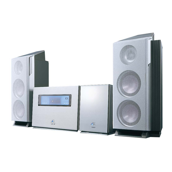
1-BIT DIGITAL AUDIO SYSTEM
SD-NX10W
MODEL
SD-NX10W 1-bit Digital Audio System consisting of SD-NX10W
(MD/CD/TUNER unit), SD-NX10W (amplifier unit) and CP-NX10W
(speaker system).
• In the interests of user-safety the set should be restored to its original
condition and only parts identical to those specified should be used.
The power of this unit is supplied from the amplifying unit via the
system connection cable. It does not operate by itself.
This document has been published to be used
for after sales service only.
The contents are subject to change without notice.
SD-NX10W
No. S3119SDNX10W/
Page
Advertisement
Table of Contents

Related Manuals for Sharp SD-NX10W


Summary of Contents for Sharp SD-NX10W
-
Page 1: Table Of Contents
No. S3119SDNX10W/ 1-BIT DIGITAL AUDIO SYSTEM SD-NX10W MODEL SD-NX10W 1-bit Digital Audio System consisting of SD-NX10W (MD/CD/TUNER unit), SD-NX10W (amplifier unit) and CP-NX10W (speaker system). • In the interests of user-safety the set should be restored to its original condition and only parts identical to those specified should be used. -
Page 2: Safety Precaution For Service Manual
SD-NX10W SAFETY PRECAUTION FOR SERVICE MANUAL The AEL (ACCESSIBLE EMISSION LEVEL) of the laser power output is less than class 1 but the laser component is capable of emitting radiation exceeding the limit for class 1. Therefore it is important that the following precautions are observer during servicing to protect your eyes against exposure to the laser beam. -
Page 3: Voltage Selection
Line output: 500 mV/47 kohms Frequency range FM: 88 - 108 MHz Headphones: 16 - 50 ohms (recommended: 32 ohms) AM: 531 - 1,602 kHz System control (SD-NX10W amplifier unit only) Amplifier unit CP-NX10W System input (RCA) Speakers; 6 ohms... -
Page 4: Names Of Parts
SD-NX10W NAMES OF PARTS SD-NX10W MD/CD/tuner unit front panel 1. CD Eject Button 1 2 3 10 11 2. CD Stop Button 3. CD Play/Pause Button 4. CD Fast Reverse/Tuning Down Button 5. CD Fast Forward/Tuning Up Button 6. MD Record Button 7. - Page 5 SD-NX10W MD/CD/tuner unit rear panel 1. Headphone Socket 2. Digital Input Socket 3. System Control Socket 4. System Output Sockets 5. Line Output Sockets 6. Auxiliary Input Sockets 7. Span Selector Switch 8. FM 75 Ohms Aerial Socket 9. Aerial Earth Terminal 10.
- Page 6 SD-NX10W Remote control 1. Remote Control Transmitter 2. CD/MD Play Mode Select Button 3. MD Record Mode Button 4. On/Stand-by Button 5. MD Record Button 6. Top Position Button 7. Track Edit Button 8. Sound Synchronise Record Button 9. Volume Up or Down Buttons 10.
-
Page 7: Operation Manual
SD-NX10W OPERATION MANUAL Setting the Clock Press the REC LEVEL/CURSOR button to adjust the date, and then press the ENTER button. Press the REC LEVEL/CURSOR button to adjust the hour, and then press the ENTER button. Press the REC LEVEL/CURSOR or button to adjust the minutes, and then press the ENTER button. - Page 8 SD-NX10W System Connections Setting the AC voltage selector Connecting the AC power lead Check the setting of the AC voltage selector located on the rear panel before plug- After making all connections, plug the unit. If you plug the unit first, the unit ging the unit into an AC socket.
- Page 9 SD-NX10W Troubleshooting Chart Many potential "problems" can be resolved by the owner without calling a service MiniDisc technician. General Symptom Possible cause A recording cannot be made. Is the MiniDisc protected against accidental Symptom Possible cause erasure? "TIME ADJUST" appears when the Did a power failure occur? Reset the clock.
- Page 10 SD-NX10W Error Messages When an error message is displayed, proceed as follows: Error messages Meaning Remedy Error messages Meaning Remedy BLANK MD Nothing is recorded. (Neither Replace it with another disc. MD NO DISC A MiniDisc has not been load- Load a MiniDisc.
-
Page 11: Disassembly
4. Socket ....(T4) x2 Jack PWB Jack PWB * (Note 1) Main PWB Screws are covered. Remove the cushion covers first with a sharp- (E2)x2 (D3)x1 ended stick and then screws. Be careful not to damage them when removing. They will be reused. - Page 12 SD-NX10W LED B PWB MD Mechanism Front (L1)x1 Decoration Unit Panel (M1)x1 CD Mechanism Lighting ø3x6mm Ass'y Plate (L1)x1 (F1)x1 ø3x8mm (L2)x4 ø3x10mm Lug Wire LED A MD/CD Block (M1)x6 ø3x6mm (M1)x1 ø3x6mm Front Cabinet Lug Wire (M2)x1 (F1)x3 (F1)x1 ø3x10mm...
- Page 13 SD-NX10W SD-NX10W (AMPLIFIER UNIT) (T1)x1 Shield Case, Top ø 2x3mm STEP REMOVAL PROCEDURE FIGURE Leg Cabinet 1. Screw ....(A1) x5 13-3 (T1)x1 ø 2x3mm Rear Cabinet 1. Screw ....(B1) x11 13-3 Front Cabinet 1. Screw ....(C1) x6...
- Page 14 SD-NX10W (D2)x1 (J1)x4 (E2)x1 ø3x10mm (E2)x1 Power (E2)x1 (E2)x1 Power 1-Bit Amp Terminal Unit (D1)x1 ø3x10mm (D1)x3 ø3x8mm Power Trans 1-Bit Amp PWB Rear Panel Figure 14-4 CP-NX10W (D1)x2 STEP REMOVAL PROCEDURE FIGURE ø3x8mm (E1)x2 Woofer 1. Leg Cushion ..(A1) x4 14-5 ø3x8mm...
-
Page 15: Removing And Reinstalling The Main Parts
SD-NX10W REMOVING AND REINSTALLING THE MAIN PARTS MD MECHANISM SECTION (A1)x1 Perform steps 1 to 4, 6, 15, 17 and 18 of the disassembly ø1.7x5mm method to remove the MD mechanism. (See pages 11 to 13.) Magnetic Head Caution: After pulling out the optical pickup connector, wrap the end of the connector in conductive aluminium foil to prevent the optical pickup from being destroyed by static electricity. - Page 16 SD-NX10W CD MECHANISM SECTION Perform steps 1 to 4, 6, 15 and 16 of the disassembly method to remove the CD mechanism. (See pages 11 to 13.) Unless the unit enters the loading completed state, the CD mechanism section can not be disassembled. It can be disassembled if an 8-cm disc is loaded.
- Page 17 SD-NX10W How to remove the CD servo PWB/optical pickup CD Servo PWB (See Fig. 17-1 to 17-3) (A2)x1 (A1)x2 1. Remove the screws (A1) x 2 pcs. ø2.5x4mm 2. Remove the flat cables (A2) x 2 pcs. 3. Remove the solder joints (A3) x 8 pcs.
- Page 18 SD-NX10W How to remove CD spindle motor How to eject CD unit (See Fig. 18-4) (See Fig. 18-1 and 18-2) 1. Unsolder the loading motor lead wire, connect the black lead wire to + and red lead wire to GND, and apply +5 V to 1.
-
Page 19: Wiring Process Diagram
SD-NX10W WIRING PROCESS DIAGRAM 1-BIT SECTION Nylon Band Nylon Band Core Core Nylon Band Nylon Band Figure 19-1 ADJUSTMENT TUNER SECTION TEST MODE fL: Low-range frequency When the tuner test mode is set, the initial setting of frequencies fC: Middle-range frequency is stored in the preset memory as shown in Table 1. - Page 20 SD-NX10W MD SECTION Enter the test mode, adjust or set as shown in the following table according to the repair operations. Execution item Checking Writing the Writing the TEMP AUTO-YOBI AUTO- AUTO-AFB Operation check EEPROM EEPROM basic EEPROM required adjustment...
- Page 21 SD-NX10W 2. Test Mode Test mode setting method 1. While the +10 forward button (+10) and the REC LEVEL/MD Fast Forward button ( ) are pressed down together, press the POWER button and then MD PLAY button. (State A is changed to state B .) 2.
- Page 22 SD-NX10W 1. EJECT mode Step No. Setting Method Remarks Display Step 1 Test mode EJECT state [ _ _ E J E C T _ _ _ ] Step 2 Press the CD STOP button. Playback power output state [ p p w _ _ _ _ _ _ _ ] Step 3 Press the CD STOP button.
- Page 23 SD-NX10W 4. AUTO AFB adjustment mode Step No. Setting Method Remarks Display Step 1 Test mode STOP state [ t s m Step 2 Press the CD PLAY button two times. AUTO AFB adjustment menu [ _ A U T _ A F B _ _ ] Step 3 Press once the MD PLAY button.
- Page 24 SD-NX10W c) Tracking setting Step No. Setting Method Display Step 1 Test mode STOP state [ t s m Step 2 Press the CD PLAY button eight times. [ E E P R O M_ S E T ] Step 3 Press the MD PLAY button.
- Page 25 SD-NX10W e) TEMP setting Setting Method Display Step No. Step 1 EJECT state (or state without mechanism) [ _ _ E J E C T _ _ _ ] Step 2 Press the TUNER (BAND) button. [ T E M P_ •...
- Page 26 SD-NX10W h) REC bit setting Display Step No. Setting Method Step 1 Test mode STOP state [ t s m Step 2 Press the CD PLAY button eight times. [ E E P R O M_ S E T ] Step 3 Press the MD PLAY button.
- Page 27 SD-NX10W 1 1 1 1 1 Adjustment Load a high-reflective TYGS1 test disc. Note: Adjust the position of the lead-in switch between FF85 to FFD2. 1. Loosen the screw (A1) x 1 pc., fixing the mechanism switch PWB. 2. Retighten the screw while pushing the PWB in the direction of arrow A if the switch position is at FF85 or lower, or in the direction of arrow B if it is at FFD2 or higher, and measure its position again.
- Page 28 SD-NX10W From Magnetic Head 2 Pin Extension Connector QCNWK0129AFZZ From Mechanism Switch PWB 28 Pin Extension Flat Cable Extension PWB for service QCNWK0108AFZZ (RUNTK0532AFZZ) Fit the exrension PWB for service to the mechanism MD Main PWB 6 Pin Extension Flat Cable...
-
Page 29: Error Message List
SD-NX10W ERROR MESSAGE LIST MD error messages Error Display Error Message Remarks Can't REC • Errors occurred 10 times continuously in the REC-PLAY • Check for scratch, dust, fingerprints, or black spots on mode. the disc. Check that the disc is not eccentric or largely •... -
Page 30: Eeprom Writing Procedure
SD-NX10W The details description of mechanism error HINF Error Display Error Message (93 Pin of IC1401) E r - M D 1 Cannot eject the disc. EJECT complete position < 1.0 V E r - M D 2 The head does not ascend. - Page 31 SD-NX10W Tracking setting Control setting Item indication Setting Item indication Setting C O N T R L 1 C O N T R L 2 T G 2 A D J T T M T F 0 H D E Q A D...
-
Page 32: Description Of Circuit For 1-Bit Unit
SD-NX10W DESCRIPTION OF CIRCUIT FOR 1-BIT UNIT (SEE THE WIRING DIAGRAMS ON PAGES 70 AND 71.) Output of gate driver Input Signals over certain level input from BIA106 are sliced into The level-shifted signals are input to the gate driver IC (HIP2100). -
Page 33: To Check And Cancel Protect Circuit Detection Line
SD-NX10W TO CHECK AND CANCEL PROTECT CIRCUIT DETECTION LINE 3 3 3 3 3 1. After power supply, the microcomputer (ICD01) built in this Excessive main supply current of 1-bit amplifier model consecutively monitors the following errors After disconnecting the CNP801 (main power source... -
Page 34: Test Mode
SD-NX10W TEST MODE From power off state to TEST mode Press the +10 Track Up button (+10) and MD REC LEVEL/MD Fast Forward button ( ) simultaneously while the POWER button of the main unit is on to obtain the TEST mode. Initially, the version is displayed. - Page 35 SD-NX10W Test mode version display With MD-SKIP-UP button MD-SKIP-DWN Version display to CD-PLAY MD-SKIP-UP MD-SKIP-DWN Version display to MD-PLAY MD-SKIP-DWN MD-SKIP-UP Version display to ERASE MD-SKIP-UP MD-SKIP-DWN Version display to MD-REC MD-SKIP-UP MD-SKIP-DWN Version display to AUX(DEMO) MD-SKIP-DWN MD-SKIP-UP Version display...
- Page 36 SD-NX10W 1. CD test Outline: Read-out of the set value after automatic adjustment (for judging difference from initial value) Forced operation of pickup (Inner/Outer circumference feed) During the PLAY mode, the number of errors accumulated for 10 seconds (750 frames) is displayed.
- Page 37 SD-NX10W Double-speed mode Press the MD-REC button in the stop mode to switch to the double/constant-speed mode cyclically. During the double-speed mode, a flag mark lights up. CD TEST N: NORMAL SPEED H: HIGH SPEED STEP NO Display Time Display...
- Page 38 SD-NX10W 5. AUX test mode Outline: To test the AUX operation Operation a. Press the VOL-UP/DOWN button. MIN (0) ←→ 1 ←→ 250 ←→ MAX (40) (The volume can be switched among 4 levels.) b. Switching of the graphic equalizer and switching test for X-BASS ON/OFF and SURROUND ON/OFF are possible.
- Page 39 SD-NX10W MD power ON time chart Power-on sequence for the MD unit (when resetting or starting it : no disc) (System side) POWER-ON CN1501 DVDD CN1501 BACK UP Power failure recovery interruption input and 3.2 V application to the MD unit...
- Page 40 SD-NX10W Power-on sequence for the MD unit (when resetting or starting it : DISC IN or disc existence) (System side) POWER-ON CN1501 As quick as possible DVDD CN1501 BACK UP Power failure recovery interruption input and 3.2 V application to the MD unit...
-
Page 41: Notes On Schematic Diagram
SD-NX10W NOTES ON SCHEMATIC DIAGRAM • Resistor: • Schematic diagram and Wiring Side of P.W.Board for this To differentiate the units of resistors, such symbol as K and model are subject to change for improvement without prior M are used: the symbol K means 1000 ohm and the symbol notice. -
Page 42: Block Diagram
SD-NX10W FLD01 8.3886MHz XLD01 +B12 PHCU01 +B5(5V) MD_DISC_IN MD_DISC_IN DR_OP_IN DR_OP_IN MD DISC DR_CL_IN DR_CL_IN IN SW TIMER_LED LEDD02 SWD23 OPEN/CLOSE ICD01 OPEN IX0381AW SYSTEM MICROCOMPUTER SWD02~SWD21 ICU03 SWD24 +B4(8V) TA7291S RESE CLOSE LOADING MOTOR DRIVER RMD01 REMOTE SENSOR –... - Page 43 SD-NX10W TO MD SECTION CNPU04 +B6(5V) VOLTAGE CNPU07 REGULATOR LRCK DATA ICU04 BCCK +B11(5V CD) 74VHC08F DATA BCCK INVERTOR LRCK 59 57 12 13 ICU05 +B11(5V CD) LC89051V DIGITAL AUDIO INTERFACE MD_LOADSW VOLTAGE MD_ST REGULATOR CNPU08 MD_SERCH ICU02 CD DIGITAL SIGNAL...
- Page 44 SD-NX10W JTP01 SYSTEM OUT/ CNP603 LINE OUT/AUX IN LINE_MUTE TERMINAL L_PRE_OUT L-CH SYSTEM OUT R_PRE_OUT R-CH R__REC_OUT R-CH L__REC_OUT LINE OUT QP07 MUTE L-CH BUFFER QP06 QP08 DRIVE –B2(–12V) R_AUX_IN R-CH AUX IN L_AUX_IN L-CH +B7(+12V) BI650 D-OUT IC650 TORX178A...
- Page 45 SD-NX10W SLICE LEVEL SET VOLTAGE +5 V OUTPUT OFFSET ADJUSTMENT ICA100 IX2815AF 7TH ORDER ∆∑ MODULATION CONVERSION LSI Figure 45 BLOCK DIAGRAM (4/7) – 45 –...
- Page 46 SD-NX10W TO 1BIT AMP TO 1BIT AMP JT900 SECTION SECTION SYSTEM IN TERMINAL L-CH R-CH SOV90 SYSTEM CONTROL CNPV98 TERMINAL CNPV99 DC DETECT DC DETECT QV96 QV98 QV95 CNP801 –B1 RL800 RELAY PROTECT DRIVE DRIVE Q803 – QV99 + –...
- Page 47 SD-NX10W SOV99 SPEAKER TERMINAL L-CH – – SP RELAY RLV99 R-CH DRIVE SP_RELAY QV92 FAN_L +B CONT DC DETECT AD RESET QV97 QV95 FAN LOW ICV91 SPEED BU2092F SWITCHING INPUT/OUTPUT EXPANDER CLOCK QV93 PROTECT DRIVE DATA AT FAN STOP M905...
- Page 48 SD-NX10W TO MAIN UNIT TO CD UNIT 1 2 3 4 5 6 7 8 9 10 11 12 13 14 15 16 17 18 19 20 21 22 23 24 25 26 27 28 CN1501 1 2 3 4...
-
Page 49: Wiring Side Of P.w.board
SD-NX10W P51 12 - D P50 2 - B TO MAIN PWB TO MAIN PWB CNPU06 CNPU08 FWC01 CNSU08 CD SERVO PWB-F (Replaced with the finished PWB) P59 7 - F TO MD MAIN PWB CN1101 P59 8 - A... - Page 50 SD-NX10W P52 6 - C P59 11 - A FROM CD CN1502 SWITCH PWB P49 2 - A TO MD MAIN CNSD01 FROM CD SERVO PWB CNSU07 CW1502 CNSU08 P52 4 - C FROM JACK PWB CNS650 RE02 ICU04 RE06...
- Page 51 SD-NX10W MAIN PWB-A1 RE26 ICU03 ICD03 QD01 27 29 31 33 35 37 39 41 43 45 47 49 51 53 55 57 59 3 2 1 28 30 32 34 36 38 40 42 44 46 48 50 52 54 56 58...
- Page 52 SD-NX10W CD SWITCH PWB-A3 CNS605 TO MD CHASSIS GND CNP605 C605 C611 (259) C652 R603 (263) LP01 C659 TO FRONT SWD09 SWD02 CABINET GND CD EJECT CP32 STAND-BY JHP01 RD85 RD90 HEADPHONES T601 SWD03 POWER TRANSFORMER TUNER C608 D606 (BAND)
- Page 53 SD-NX10W MD SENSOR MD LOADING PWB-A7 PWB-E2 RU88 SW1934 PLAY M903 MD LOADING MOTOR 1 2 3 TP1972 CNSU11 SW1933 SW1932 LOADING RECORD TP1971 TP1973 TP1974 SOCKET TP1975 PWB-A6 P59 12 - D CN1401 TO MD MAIN PWB CW1931 CNPU12...
- Page 54 SD-NX10W C802 C800 C805 C807 C803 RV84 CNP806 C806 RV85 CNP801 3 2 1 RV97 1 2 3 4 5 6 7 8 7 6 5 4 3 2 1 CNP804 CNP805 RV96 RL800 CNSA111 P56 2 - A FROM...
- Page 55 SD-NX10W TERMINAL PWB-B3 DV93 SOV99 SPEAKER TERMINALS L-CH QV92 RV62 – E C B RV64 RV57 RV61 R-CH RV63 RLV99 – DV90 QV94 QV97 DV89 RV37 CV83 RV39 RV40 RV38 RV41 SOV90 SYSTEM RV42 CONTROL TERMINAL DV86 CV07 CV82 RV47...
- Page 56 SD-NX10W P54 5 - C P55 10 - D TO POWER PWB TO TERMINAL PWB CNP801 CNPV99 CNSA111 CNSA110 CORA03 CORA01 LFA04 BIA111 BIA110 LFA05 RA341 LFA03 LFA06 CA224 RA340 ICA105 CA223 LA102 CA150 QA103 DA131 CA179 QA102 LA106 RA130...
- Page 57 SD-NX10W RD ( R) W H (W ) COLOR TABLE ORANGE YELLOW GREEN BLUE VIOLET GRAY BLACK PINK BROWN WHITE ICA103 ICA104 ICA101 ICA102 CA121 CA128 CA118 CA131 RA170 CA126 RA120 ICA110 DA107 CA112 DA106 CA113 RA119 CA114 RA108 CA104 1-BIT AMP PWB-D (TOP VIEW) Figure 57 WIRING SIDE OF P.W.BOARD (9/11)
- Page 58 SD-NX10W C1707 IC1702 C1509 R1704 C1606 L1552 Q1702 Q1700 R1516 C1304 R1513 R1561 L1551 R1511 Q1701 R1705 L1702 R1703 C1701 C1712 C1704 C1716 C1702 L1701 C1710 R1712 R1711 C1803 C1800 R1714 C1700 C1711 C1714 C1501 R1612 R1808 R1614 Q1800 C1802...
- Page 59 SD-NX10W P50 1 - E TO MAIN PWB CNPU04 P49 5 - E TO MAGNET HEAD P50 5 - A CW1501 CW1903 FROM MAIN PWB CW1502 TP1543 TP1702 TP1301 CN1300 CN1501 TP1524 TP1518 CN1502 TP1517 TP1525 TP1300 TP1515 R1535 R1537...
-
Page 60: Schematic Diagram
SD-NX10W MD SENSOR OPEN/CLOSE PWB-A7 SWITCH PWB-A5 MD DISC SWD23 IN SW OPEN/CLOSE 5.08V CLOSE OPEN FLD01 FL DISPLAY RU89 BIU11 BIU12 ICU03 TA7291S CNSU11 CNSU12 LOADING MOTOR DRIVER CNPU12 CNPU11 80 79 78 77 76 75 74 73 72 71 70 69 68 67 66 65... - Page 61 SD-NX10W MAIN PWB-A1(1/3) +8V_CD GND_CD1 CD03 1/50 BUCK CD02 1/50 BUS3 BUS2 CD01 1/50 BUS1 INVERTER BUS0 QD01 CD_SENS_A RE60 KRC107M 3.95V CD_RESET CD_SENS_B 73 72 71 70 69 68 67 66 65 64 63 62 61 60 59 58 57...
- Page 62 SD-NX10W FM SIGNAL RECORD SIGNAL AUX SIGNAL MD SIGNAL +8V_CD GND_CD1 BUCK BUS3 BUS2 BUS1 BUS0 CD_SENS_A CD_RESET CD_SENS_B CD_SENS_C CD_CHK_SW LOAD_M+ LOAD_M- TUN_MUTE TUN_ST/SD HP_SW LINE_MUTE POWER MD_ST SYS_MUTE QD08 MD_RESET KTC3199GR MD_DATA_ CD_FNUC RE44 RE47 4.7K MD_KDATA MD_DSCK...
- Page 63 SD-NX10W MAIN PWB-A1(2/3) CNSU01 CU33 100/10 HP_SW +5V_CD ZDU03 RU30 DZ10BSB ICU01 SPAN LC75341M CU32 100/16 AUDIO PROCESSOR CU31 0.022 LCK2 RU31 DU01 RU34 RU33 DS1SS133 GND_D RU32 CU45 PROTECT (OS-CON) 100/10 VREF LINE_MUTE CU30 CU17 RU12 22/16 0.33/50 R_A/P_OUT...
- Page 64 SD-NX10W AUX SIGNAL FM SIGNAL LINE_MUTE CS02 0.27 R_A/P_OUT SURROUND RS12 RS04 RS06 SWITCHING 4.7K QS01 DS01 RS02 KRA107M DS1SS133 CS08 SUR_ON/OFF 0.33 MUTE 11.1V RP08 RS10 CS06 DRIVE 4.7K 100K –11V 0.0047 QS02 11.2V 2SK246GR –B RS08 QP02 100K...
- Page 65 SD-NX10W CNSU03 LINE_MUTE L_PRE_OUT GND_A CP02 RP02 1/50 R_PRE_OUT MUTE RP56 CP06 RP04 DRIVE 100K 100P 4.7K –B –B RP27 CP13 CP11 47/25 0.022 ICP01 NJM4580M CP12 CP14 BUFFER AMP. 47/25 0.022 RP61 RP03 RP55 RP28 CP05 4.7K 100K 100P...
- Page 66 SD-NX10W AUX SIGNAL FM SIGNAL CNP603 LINE_MUTE_ L_PRE_OUT_ CP09 10/16 GND_A2_ R_PRE_OUT_ CP10 10/16 R_REC_OUT_ GND_A1_ L_REC_OUT_ –12V(A)_ –12V(A)_ –B R_AUX_IN_ GND_A__ L_AUX_IN_ +12V(A)_ +12V(A)_ CNP601 HP_SW_ +5V_CD_ SPAN_ PROTECT DRIVE Q606 CLK_ R625 KRA107M LCK2_ 0.8V PROTECT_ 4.9V 4.9V...
- Page 67 SD-NX10W JACK PWB-A2 JTP01 SYSTEM OUT/ LINE OUT/AUX IN TERMINAL L-CH RP05 CP15 RP11 100K 220P SYSTEM OUT RP06 CP16 RP12 100K 220P R-CH RP32 RP64 QP07, QP08: MUTE DRIVE R-CH CP36 QP08 2.2/50 2SC2878B RP54 RP52 CP38 QP06 100K...
- Page 68 SD-NX10W P71 9 - A P71 12 - E FROM FROM 1-BIT AMP PWB 1-BIT AMP PWB JT900 SYSTEM IN CNSA106 CNSA110 TERMINAL L-CH R-CH 4 5 6 10 11 12 13 CNPV99 CNPV98 CV09 SOV90 0.0022(ML) SYSTEM CONTROL TERMINAL...
- Page 69 SD-NX10W CV09 TERMINAL PWB-B3 022(ML) CV84 FM SIGNAL 0.001(ML) L-CH SOV99 – ICV91 SPEAKER TERMINAL BU2092F R-CH RLV99 – INPUT/OUTPUT RV59 RV58 QV97 EXPANDER SP_RELAY QV95 KTC3199GR FAN_L KTC3199GR RV57 SP RELAY +B CONT DV87 DV88 DRIVE CV73 DS1SS133 AD RESET...
- Page 70 SD-NX10W 1-BIT AMP PWB-D FM SIGNAL R-CH ANALOG IN R-CH L-CH RA174 8.2K ANALOG IN L-CH RA173 8.2K –B RA176 2.2K DA129 DA126 –B 1SS361 1SS361 RA177 DA127 DA128 CA182 TEST RA179 1SS361 1SS361 CA185 0.001 GNDX CA194 RA181 RA183...
- Page 71 SD-NX10W R-CH_IN P68 4 - A LA127 LA124 AGND CNPV98 L-CH_IN TO TERMINAL PWB CA211 CNSA106 CA214 0.001 LFA01 6.75µH CORA02 CA196 A+5V 47/25 AGND_AD P68 1 - F D+5V CA182 CNP802 DGND_AD CA197 TO POWER PWB 47/25 RESET LFA02 CNSA112 6.75µH...
- Page 72 SD-NX10W MD SIGNAL RECORD SIGNAL TP1131 C1113 C1117 C1119 0.47 R1119 C1112 220K TP1202 TP1116 (CH) 100 99 98 97 96 95 94 93 9 1234 VCC1 EFMAGC C1201 TP1201 EFMO-I ADAGI EFMO-I AGND1 ADAGC AVCC2 C1211 EFMMO DIFF C1121...
- Page 73 SD-NX10W MD MAIN PWB-C TP1202 100 99 98 97 96 95 94 93 92 91 90 89 88 87 86 85 84 83 82 81 80 79 78 77 76 TP1212 DADATA EFMO-I ADDATA R1211 DFCK DFCK AGND1 BCLK AVCC2...
-
Page 74: Voltage
SD-NX10W VOLTAGE IC800 ICV91 ICD01 IC1101 IC1201 IC1401 NO. VOLTAGE NO. VOLTAGE NO. VOLTAGE NO. VOLTAGE NO. VOLTAGE NO. VOLTAGE NO. VOLTAGE NO. VOLTAGE NO. VOLTAGE 5.4 V 4.96 V –29.5 V 0.7 V 1.3 V 1.6 V –29.5 V –... -
Page 75: Waveforms Of 1-Bit Circuit
SD-NX10W WAVEFORMS OF 1-BIT CIRCUIT 2.00 V/div 2.00 V/div 2.00 V/div 2.00 V/div AD IC Output LEVEL SHIFT OUT + Side POWER SUPPLY - Side 194.545465 µs 500 ns/div 520 mV 194.545465 µs 500 ns/div -12.47 V Amplitude Waveform after level shift... -
Page 76: Waveforms Of Md Circuit
SD-NX10W WAVEFORMS OF MD CIRCUIT POWER ON TOC READ (Low reflection disc) TP1122 (F+) TP1518 (RESET) TP1207 (TEMON) TP1603 TP1800 (SP+) (3.2V) TP1602 TP1511 (SP-) (PCONT0) TOC READ (High reflection disc) TOC READ (Low reflection disc) TP1122 TP1122 (F+) (F+) - Page 77 SD-NX10W PLAY (Low reflection disc) TP1201 (EFMMON) TP1300 (REC HEAD) TP1207 (TEMON) TP1302 (EFMO) TP1121 (T+) TP1105 (LDVAL) TP1421 (CIN) TP1113 (R/P) PLAY (High reflection disc) Analog REC TP1201 (EFMMON) IC1201 (DFCK) TP1207 (TEMON) IC1201 (ADDATA) TP1121 (T+) IC1201 (BCLK)
-
Page 78: Cd Optical Pickup Lens Cleaning
SD-NX10W CD OPTICAL PICKUP LENS CLEANING When the CD does not function When the CD section does not operate when the objective lens of the optical pickup is dirty, this section may not operate. Clean the objective lens, and check the playback operation. When this section does not operate even after the above step is taken, check the following items. -
Page 79: Troubleshooting
SD-NX10W TROUBLESHOOTING Preparations If dusts and foreign materials are accumulated on the pickup lens, playback sounds can be skipped or the TOC (Table of Contents) can't be displayed. Clean the object lens and check the playback. When lens are dirty, do the following. - Page 80 SD-NX10W • Disc loading is not normal. Is disc loaded when it is inserted ? Check the power PWB, main PWB, and Is +5 V to +6 V applied to the pins 6 and 7 of CN1501 ? CN1501. Is pulse input in the pin 22 of CN1501 when reset power Check the main PWB and CN1501.
- Page 81 SD-NX10W • Normal playback. When it has been confirmed that EEPROM value is normal in the TEST mode. Is initialization performed normally when high reflection disc is Does the playback time display advance ? played back ? Check IC1201. Does disc rotate normally ?
- Page 82 SD-NX10W Check in the test mode. • The spindle motor does not rotate. Is waveform output from the pins 25 of IC1201 in the step 4 of Check the pins 25 of IC1201, soldering of peripheral circuit, and parts. AUTO auxiliary adjustment mode of TEST mode ? Is waveform output from the pins 9 and 10 of IC1601 and the Check IC1601, CN1402, and soldering of mechanism switch PWB.
-
Page 83: Function Table Of Ic
SD-NX10W FUNCTION TABLE OF IC ICU01 VHiLC75341M-1: Audio Processor (LC75341M) Pin No. Terminal Name Function Serial data and clock input terminal for control. Chip enable terminal. When changing from "H" to "L", data is written in the internal latch and each analog switch is turned on. - Page 84 SD-NX10W ICA100 RH-iX2815AFZZ: 7th Order Modulation Conversion LSI (IX2815AF) Pin No. Port Name Input/Output Function VDDL Input L channel digital output section power terminal. OUTL (+) Output L channel forward output terminal. OUTL (–) Output L channel reverse output terminal.
- Page 85 SD-NX10W ICD01 RH-iX0381AWZZ: System Microcomputer (IX0381AW) (1/2) Terminal Name Port Name Input/Output Remarks P77/AN7 SD_ST_IN Input Tuner tuning and stereo receiver signal detection. (A/D Input) Not tuned: "H", SD input: "M", ST: "L" P76/AN6 KEY1 Input (A/D Input) A/D KEY input 1.
- Page 86 SD-NX10W ICD01 RH-iX0381AWZZ: System Microcomputer (IX0381AW) (2/2) Terminal Name Port Name Input/Output Remarks X_IN Input Reference oscillation input. 8.38 MHz crystal connection. XOUT X_OUT Output Reference oscillation output. 8.38 MHz crystal connection. — Connected to GND. IC_LCK2 Output External control IC related latch clock output.
- Page 87 SD-NX10W ICD02 VHiBU2092F/-1: Input/Output Expander (BU2092F) Pin No. Terminal Name Port Name Function DATA Serial data input. CLOCK Data shift clock. LCK2 Data latch clock. LINE_MUTE Line mute. "L"= MUTE ON, "H"= MUTE OFF CD_FUNC CD function. "H"= Except CD function, "L"= CD function SP_RLY Speaker relay.
- Page 88 SD-NX10W IC1101 VHiiR3R58M/-1: RF Signal Processor (IR3R58M) Function Terminal Name Pin No. RF signal input terminal 1. Input of RF signal output of pickup. RF signal input terminal 2. Input of RF signal output of pickup. RF signal input terminal 3. Input of RF signal output of pickup.
- Page 89 SD-NX10W IC1101 VHiiR3R58M/-1: RF Signal Processor (IR3R58M) ADAGI EFM AGC ADAGC DIFF ADIPNF ADIP AGC REFI ADIPO BIAS REFO GND2 AOUT VCC2 OPICPW MODE DISC SGAIN BOUT DTEMP IC1201 VHiLR37816A-1: Endec/Atrac (LR37816A) 75 74 73 72 71 70 69 68 67 66 65 64 63 62 61 60 59 58 57 56 55 54 53 52 51...
- Page 90 SD-NX10W IC1201 VHiLR37816A-1: Endec/Atrac (LR37816A) (1/2) Terminal Name Input/Output Function Pin No. EFMMON Output EFM monitor output. AVCC1 Input Analog power supply. (for EFM system 8AD, 8DA) EFMI Input EFM signal input from RF amplifier. AGND1 — Analog GND. AVCC2 Input Analog power supply.
- Page 91 SD-NX10W IC1201 VHiLR37816A-1: Endec/Atrac (LR37816A) (2/2) Terminal Name Input/Output Function Pin No. TCRS Output Track cross signal. TEST0 Input Input for test. Connected to GND if used normally. TEST1 Input Input for test. Connected to GND if used normally. DILOCK Output DIN lock detection.
- Page 92 SD-NX10W IC1202 RH-iX2474AFZZ: 4Mbit D-RAM (IX2474AF) Function Terminal Name Pin No. 1, 2 DQ0, DQ1 Data input/Data output. Write enable. Row address strobe. Address input. A0-A3 Address input. Power (3.3 V) 11-15 A4-A8 Address input. Output enable. Column address strobe.
- Page 93 SD-NX10W IC1401 RH-iX0410AWZZ: MD System Microcomputer (IX0410AW) (1/2) Terminal Name Input/Output Function Pin No. 4M/16M Output 4 M/16 M DRAM selection input. Output 64 M DRAM selection input. LDVAR Output LDVAR (laser power adjustment output) ADJS Output ADJS (for automatic adjustment step check)
- Page 94 SD-NX10W IC1401 RH-iX0410AWZZ: MD System Microcomputer (IX0410AW) (2/2) Terminal Name Input/Output Pin No. Function SYS D2 Input/Output SYS D2 (data bus 2) SYS D1 Input/Output SYS D1 (data bus 1) SYS D0 Input/Output SYS D0 (data bus 0) SLOT1 Output...
- Page 95 SD-NX10W IC1701 VHiUDA1345/-1: AD/DA Converter (UDA1345) Terminal Name Pin No. Function VSSA AD converter analog ground. VDDA AD converter analog power. VINL AD converter input. (left) VREFA AD converter reference voltage. VINR AD converter input. (right) VADCN AD converter reference voltage N.
-
Page 96: Fl Display
SD-NX10W FL DISPLAY FLD01: VVKHNA13LS3-1 13G 12G 11G 10G 9G – 12 – 4 GROUP DISC TOTAL TRACK DATE CLOCK OVER SURROUND RANDOM STEREO PROGRAM SLEEP MONO GROUP S-SYNC T-EDIT TIMER PTYI PLAY REC (3G – 13G) CONNECTION PIN No. 59 CONNECTION PIN No. - Page 97 PARTS GUIDE 1-BIT DIGITAL AUDIO SYSTEM SD-NX10W MODEL SD-NX10W 1-bit Digital Audio System consisting of SD-NX10W (MD/CD/TUNER unit), SD-NX10W (amplifier unit) and CP-NX10W (speaker system). “HOW TO ORDER REPLACEMENT PARTS” To have your order filled promptly and correctly, please furnish the For U.S.A.
- Page 98 SD-NX10W PRICE PRICE DESCRIPTION PARTS CODE PARTS CODE DESCRIPTION RANK RANK QD01 VSKRC107M//-1 AC Digital,NPN,KRC107 M SD-NX10W QD03~05 VSKRA107M//-1 AE Digital,PNP,KRA107 M QD06 VSKRC104M//-1 AC Digital,NPN,KRC104 M INTEGRATED CIRCUITS QD07 VSKRC107M//-1 AC Digital,NPN,KRC107 M QD08 VSKTC3199GR-1 AB Silicon,NPN,KTC3199 GR IC601...
- Page 99 SD-NX10W PRICE PRICE PARTS CODE DESCRIPTION PARTS CODE DESCRIPTION RANK RANK AB 0.47 µF,50V,Electrolytic ZDU01,02 VHEDZ3R3BSA-1 AB Zener,3.3V,DZ3.3BSA C654 VCEAEA1HW474M J AA 0.001 µF,50V ZDU03 VHEDZ100BSB-1 AB Zener,10V,DZ10BSB C655 VCKYBT1HB102K AA 0.001 µF,50V ZDV99 VHEDZ6R8BSB-1 AB Zener,6.8V,DZ6.8BSB C657 VCKYBT1HB102K AA 0.001 µF,50V...
- Page 100 SD-NX10W PRICE PRICE PARTS CODE DESCRIPTION PARTS CODE DESCRIPTION RANK RANK AB 1 µF,16V C1607 VCKYTV1CF105Z CD12~14 VCCSMN1HL470J AA 47 pF,50V AE 4.7 µF,10V C1610 RC-KZ0003AWZZ CD16,17 VCKYMN1HB101K J AA 100 pF,50V AA 0.0047 µF,50V C1611 VCKYCY1HB472K CD18 VCCSMN1HL470J AA 47 pF,50V AA 0.01 µF,16V...
- Page 101 SD-NX10W PRICE PRICE PARTS CODE DESCRIPTION PARTS CODE DESCRIPTION RANK RANK AA 0.0022 µF,16V CV80 VCTYBT1CX222M R1212 VRS-CY1JB470J AA 47 ohms,1/16W AA 0.022 µF,25V CV81 VCTYBT1EF223Z R1214 VRS-CY1JB103J AA 10 kohm,1/16W AA 0.001 µF,50V CV82 VCKYBT1HB102K R1215 VRS-CY1JB105J AA 1 Mohm,1/16W AB 33 µF,16V,Electrolytic...
- Page 102 SD-NX10W PRICE PRICE PARTS CODE DESCRIPTION PARTS CODE DESCRIPTION RANK RANK RA112~115 VRS-CY1JB222J AA 2.2 kohms,1/16W RE01 VRD-MN2BD392J AA 3.9 kohms,1/8W RA116 VRS-CY1JB103J AA 10 kohm,1/16W RE02~17 VRD-MN2BD473J AA 47 kohms,1/8W RA117~120 VRS-CY1JB224J AA 220 kohms,1/16W RE18 VRD-ST2EE561J AA 560 ohms,1/4W...
- Page 103 SD-NX10W PRICE PRICE PARTS CODE DESCRIPTION PARTS CODE DESCRIPTION RANK RANK RU81 VRD-ST2CD101J AA 100 ohm,1/6W CNP803 92LCONE2P53253 J AB Plug,2Pin RU82 VRD-MN2BD101J AA 100 ohm,1/8W CNP804 QCNCM010HAWZZ J AC Plug,8Pin RU83 VRD-ST2EE391J AA 390 ohms,1/4W CNP805 QCNCM010GAWZZ J AC Plug,7Pin...
- Page 104 SD-NX10W PRICE PRICE DESCRIPTION PARTS CODE PARTS CODE DESCRIPTION RANK RANK SWD07 92LSWICHT1663T J AC Switch,Key Type 92LCAB3514CASY J AW Top Cabinet Ass’y [CD Play/Pause] 202- 1 ———— — Top Cabinet SWD08 92LSWICHT1663T J AC Switch,Key Type [CD Stop] (Not Replacement Item)
- Page 105 SD-NX10W PRICE PRICE PARTS CODE DESCRIPTION PARTS CODE DESCRIPTION RANK RANK TSPC-0864AWZZ Label,Specifications (Amp) SPAKA0278AWZZ AH Packing Add.,Left (Amp) [Except for Australia/Thailand/ SPAKA0279AWZZ AH Packing Add.,Right (Amp) Hong Kong/Taiwan] SPAKC1199AWZZ J Packing Case TSPC-0869AWZZ Label,Specifications (Amp) SPAKT0024AWZZ AK Inner Packing Case (Main)
- Page 106 SD-NX10W PRICE PRICE DESCRIPTION PARTS CODE PARTS CODE DESCRIPTION RANK RANK CP-NX10W SPEAKER BOX PARTS 92LBA705A-R BF Front Panel,Right 92LBA705A-L BF Front Panel,Left 92LBX666-R BK Speaker Box,Right 92LBX666-L BK Speaker Box,Left 92LDL1694 AH Duct 92LDLAS1688 BD Net Frame Ass’y 92LDL1689-R...
- Page 107 SD-NX10W SD-NX10W 33x2 33x2 512x2 M903 SW1934 SW1932 SW1933 PWB-C PWB-E1 SW1931 SW1930 510x2 506x2 M902 SW1936 PWB-E2 501x2 M901 505x3 Figure 10 MD MECHANISM EXPLODED VIEW – 10 –...
- Page 108 SD-NX10W SD-NX10W (MD/CD/TUNER UNIT) 623x4 607x2 611x2 267(267-1,267-2,267-3, 267-4,267-5,267-6) Refer to pages 17 and 18 of the service manual. 611x5 612x5 607x2 611x2 611x2 611x2 608x2 MD MECHANISM UNIT 611x2 PWB-A6 608x2 611x2 268x2 612x3 613x5 FLD01 203-1 203-3 203-2...
- Page 109 SD-NX10W SD-NX10W (AMPLIFIER UNIT) 601x2 PWB-B3 PWB-B2 617x2 617x2 617x2 621x2 617x2 618x2 617x2 617x2 271x2 617x2 262x3 PWB-B4 Silicon 617x2 Grease 617x2 IC806 IC801 235x2 D800 617x2 Silicon 617x4 QA101 Grease Silicon Grease 235x2 IC802 617x2 QA100 IC804 Silicon...
- Page 110 SD-NX10W CP-NX10W SP5,6 TWEETER SP5,6 COIL 0.33mH TWEETER Capacitor COIL 4.7µF 0.33mH SP1,2 SP1,2 SPEAKER WOOFER WOOFER TERMINAL NETWORK ASS'Y SP3,4 WOOFER 921x3 SP3,4 920x4 SPEAKER 909,910 WOOFER TERMINAL 901,902 914x6 903,904 SP5,6 907,908 922x8 SP1~4 915x6 Figure 13 SPEAKER EXPLODED VIEW...
- Page 111 SD-NX10W — M E M O — – 14 –...
- Page 112 SD-NX10W © COPYRIGHT 2001 BY SHARP CORPORATION ALL RIGHTS RESERVED. No part of this publication may be reproduced, stored in a retrieval system, or transmitted in any form or by any means, electronic, mechanical, photocopying, recording, or otherwise, without prior written permission of the publisher.