Table of Contents
Advertisement
Quick Links
e
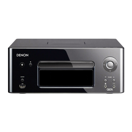
RCD-N8
• The part list can be found in a separate file.See the part list in Excel format.
• For purposes of improvement, specifications and design are subject to change without notice.
• Please use this service manual with referring to the operating instructions without fail.
• Some illustrations using in this service manual are slightly different from the actual set.
SERVICE MANUAL
MODEL
NETWORK CD RECIEVER
JP
E3
E2
P
e
D&M Holdings Inc.
Ver. 4
Please refer to the
MODIFICATION NOTICE.
E1
E1C
EA
E2R EUT
P
Advertisement
Table of Contents

Related Manuals for Denon RCD-N8


Summary of Contents for Denon RCD-N8
- Page 1 MODIFICATION NOTICE. SERVICE MANUAL MODEL E2R EUT RCD-N8 NETWORK CD RECIEVER • The part list can be found in a separate file.See the part list in Excel format. • For purposes of improvement, specifications and design are subject to change without notice.
-
Page 2: Table Of Contents
CONTENTS ABOUT THIS MANUAL .............3 ABOUT REPLACE THE MICROPROCESSOR What you can do with this manual ..........3 WITH A NEW ONE ..............40 Using Adobe Reader (Windows version) ........4 VERSION UPGRADE PROCEDURE OF FIRMWARE ....40 SAFETY PRECAUTIONS ............6 1. How to update by DISC ............40 2. -
Page 3: About This Manual
ABOUT THIS MANUAL Read the following information before using the service manual. What you can do with this manual Search for a Ref. No. (phrase) Jump to the target of a schematic diagram (Ctrl+Shift+F) connector You can use the search function in Acrobat Reader to Click the Ref. -
Page 4: Using Adobe Reader (Windows Version)
Using Adobe Reader (Windows version) Add notes to this data (Sign) Magnify schematic / printed wiring board diagrams - 1 The Sign function lets you add notes to the data in this manual. (Ctrl+Space, mouse operation) Save the file once you have finished adding notes. [Example using Adobe Reader 9,X] Press Ctrl+Space on the keyboard and drag the [Example using Adobe Reader X]... - Page 5 Magnify schematic / printed wiring board Magnify schematic / printed wiring board diagrams - 2 diagrams - 3 (Pan & Zoom function) (Loupe Tool function) The Pan & Zoom function lets you see which part of a The Loupe Tool function lets you magnify a specific magnified diagram is being shown in a separate window.
-
Page 6: Safety Precautions
SAFETY PRECAUTIONS The following items should be checked for continued protection of the customer and the service technician. LEAKAGE CURRENT CHECK Before returning the set to the customer, be sure to carry out either (1) a leakage current check or (2) a line to chassis resistance check. -
Page 7: Note For Schematic Diagram
NOTE FOR SCHEMATIC DIAGRAM WARNING: Parts indicated by the z mark have critical characteristics. Use ONLY replacement parts recommended by the manufacturer. CAUTION: Before returning the set to the customer, be sure to carry out either (1) a leakage current check or (2) a line to chassis resistance check. If the leakage current exceeds 0.5 milliamps, or if the resistance from chassis to either side of the power cord is less than 460 kohms, the set is defective. -
Page 8: Instructions For Handling Semi-Conductors And Optical Unit
INSTRUCTIONS FOR HANDLING SEMI-CONDUCTORS AND OPTICAL UNIT Electrostatic breakdown of the semi-conductors or optical pickup may occur due to a potential difference caused by electrostatic charge during unpacking or repair work. 1. Ground for Human Body Be sure to wear a grounding band (1 MΩ) that is properly grounded to remove any static electricity that may be charged on the body. -
Page 9: Specifications
SPECIFICATIONS n CD player n Wireless LAN • Audio performance Network type (wireless LAN standards): S/N ratio (1 kHz) 100 dB Conforming to IEEE 802.11b Dynamic range (1 kHz) 100 dB Conforming to IEEE 802.11g (Conforming to Wi-Fi ® )z Total harmonic distortion (1 kHz) 0.01 % Transfer rate: DS-SS: 11 / 5.5 / 1 Mbps (Automatic switching) n Audio AMP OFDM: 54 / 48 / 36 / 24 / 18 / 12 / 9 / 6 Mbps (Automatic switching) Security:... -
Page 10: Dimension
DIMENSION 280.0 30.0 35.0 210.0 35.0... -
Page 11: Caution In Servicing
CAUTION IN SERVICING ABOUT REPLACE THE WLAN MODULE WITH A NEW ONE When replaced of this Unit WLAN MODULE (E2 : 963189100410D) (JP : 963189100420D), confirm contents of the following. (1) Replace the WLAN MODULE with the (E2 : 963189100410D)(JP : 963189100420D)(MAC Address was written). (2) The firmware is updated by DPMS. -
Page 12: Initializing Network Cd Receiver
Initializing NETWORK CD RECEIVER NETWORK RECEIVER initialization should be performed when the μ-com, peripheral parts of μ-com, and Digital PCB. are replaced. 1. Turn off the power using ON/STANDBY button, unplug the power cord. 2. Plug the power cord into a power outlet while pressing VOLUME d and CURSOR i button simultaneously. (Factory Reset) 3. -
Page 13: Note Handling And Replacement Of The Laser Pick-Up
NOTE HANDLING AND REPLACEMENT OF THE LASER PICK-UP 1. Protection of the LD Short a part of the LD circuit by soldering. After connection to a circuit, remove the short solder. 2. Precautions when handling the laser CD mechanism • Handle the laser pick-up so that it is not exposed to dust. •... -
Page 14: Disassembly
DISASSEMBLY • Disassemble in order of the arrow in the following figure. • In the case of the re-assembling, assemble it in order of the reverse of the following flow. • In the case of the reassembling, observe "Caution concerning disassembly and assembly!". •... - Page 15 • Refer to the diagram below about the shooting direction of each photograph. • Photographs with no shooting direction indicated were taken from the top of the set. • The photograph is RCD-N8(E2) model. The viewpoint of each photograph (Shooting direction) Shooting direction: B [View from the top]...
-
Page 16: Top Cover
1. TOP COVER Proceeding : SIDE PANEL TOP COVER → (1) Remove the screws. Shooting direction: C Shooting direction: D (2) Remove the screws. Shooting direction: A (3) Remove the connector wire. Shooting direction: A CP303... -
Page 17: Cd Mecha Assy
2. CD MECHA ASSY Proceeding : SIDE PANEL TOP COVER → CD MECHA ASSY → (1) Remove the screws. (2) Laser short-circuit in Pick-up of CD MECHANISM ASS'Y, then disconnect the connector wires and FFC cable. Be sure to wear a grounding band. Soldering place Shooting direction: A (3) Remove the connector wire. -
Page 18: Front Panel Assy
3. FRONT PANEL ASSY TOP COVER → FRONT PANEL ASSY Proceeding : SIDE PANEL → (1) Remove the screws. View from the bottom (2) Cut the clamp bands, remove the connector wire and FFC. CP301 CON2 CON1 Shooting direction: D CP104 CN401... - Page 19 (3) Remove the screws. Shooting direction: C Shooting direction: D Please refer to "EXPLODED VIEW" for the disassembly method of FRONT PANEL ASSY.
-
Page 20: Network Pcb Assy
4. NETWORK PCB ASSY TOP COVER CD MECHA ASSY → FRONT PANEL ASSY Proceeding : SIDE PANEL → → NETWORK PCB ASSY → (1) Remove the screws. Shooting direction: A (2) Remove the screws. -
Page 21: Smps Pcb Assy
5. SMPS PCB ASSY Proceeding : SIDE PANEL TOP COVER CD MECHA ASSY → FRONT PANEL ASSY → → SMPC PCB ASSY → (1) Remove the screws. View from the bottom (2) Remove the screws. Shooting direction: C CN221 CN222... - Page 22 (3) Remove the screws. Shooting direction: C (4) Remove the screws. Shooting direction: A...
-
Page 23: Main Pcb Assy
6. MAIN PCB ASSY TOP COVER → CD MECHA ASSY Proceeding : SIDE PANEL → FRONT PANEL ASSY → NETWORK PCB ASSY MAIN PCB ASSY → → (1) Remove the screws. Shooting direction: A (2) Remove the screws. View from the bottom (3) Remove the SUPPORT MECHA. - Page 24 (4) Remove the screws, remove the connector wires. Shooting direction: C CN221 CN222...
-
Page 25: Special Mode
SPECIAL MODE Special mode setting Plug AC cord into power outlet while pressing buttons A and B. Each button continue to press until the lit of ON/STANDBY. Mode Button A Button B Contents CURSOR Initializing. Factory Reset Initialization mode (Factory Reset) VOLUME UP DOWN *Can't erase the Recently Played list... -
Page 26: Initialization Mode (Factory Reset)
1. Initialization mode (Factory Reset) Backup data initialization is carried out. Refer to Initialization Items (Default setting). After initialization, move on to normal mode. CAUTION Version information (such as rewriting failed log) Clear. Clear the history of protection. "Initial value of laser current" and "The accumulated laser on time" not cleared. Power failure flag is not cleared. -
Page 27: Initialization Mode (User Reset)
2. Initialization mode (User Reset) Backup data initialization is carried out. Refer to Initialization Items (Default setting). After initialization, move on to normal mode. CAUTION The difference is the following three points. • Version information (such as rewriting failed log) not cleared. • History of protection not cleared. •... - Page 28 Select the "Version" in the "Setup". Press 1 / 3 ENTER button The version of the System u-com. Press Cursor i The version of the boot loader System u-com. Press Cursor i The version of the boot loader Network u-com. Press Cursor i The version of the image Network u-com.
-
Page 29: Cd Test Mode
4. CD test mode Startup display "CD Test Mode" displayed for 5 seconds. CD TEST MODE display To exit this mode, unplug the power cord. 4.1. Before starting the test Open the tray and set the disc. Even if the disc is, the tray must let OPEN → CLOSE. 4.2. - Page 30 r TRACKING ON 1 / 3 ENTER button t SUB CODE readout (playback sound output) The BER (Block Error Rate) generated in 1second's time is displayed of the display. Cursor o button Cursor p button Cursor o button Cursor p button Inner (IN), Ataru Amane (MID), outer (OUT) to play go to three places, make the error count.
- Page 31 4.4. All servo on and Auto Adjustment When Cursor u button is pressed, all servos turn on, auto adjustment is performed and switch to playback operation. (Playback sound output) Stop (stop to the playback state after auto adjustment) When SOURCE button is pressed, play operation and servo stop. The following will be displayed. After stopping, conduct reading of auto adjust values.
-
Page 32: Cd Heat Run Mode
4.6. Accumulated laser on time display When the Volume f button is pressed while this Unit is in the "CD TEST MODE "displayed, the accumulated laser on time is displayed. The laser drive times are added and the result is displayed. One count corresponds to 10 minutes. - Page 33 5.2. Heat run Short mode Playing last track on disc. After disc playback has finished, then tray open and close. And playback again. The heat run repetition no. is incremented (increased by 1) when the tray is opened. Repeat this operation. [H.R. Short] displayed. Select "H.R.Short", and press 1 / 3 ENTER button.
-
Page 34: Product Mode 1
6. Product Mode 1 Startup display "Product Mode1" displayed for 5 seconds. To exit this mode, unplug the power cord. 7. Product Mode 2 Startup display "Product Mode2" displayed for 5 seconds. Tested during production to perform the following settings automatically. Sleep setting : 4 minutes Auto Standby :4 minutes Sleep setting and timer started. - Page 35 DC protect 2 Short of '+B/-B+12V_D or +12V_Aor -12V_A or +29V fail' Over current Over-current detection digital amplifier Protection history is reset. When the Cursor u button is pressed for over 5 seconds while the protection history is displayed, the count value is reset.
-
Page 36: Update Mode (By Disc)
9. Update mode (by disc) Firmware update disc by. When you replace this Unit‘s WLAN MODULE (CX870), you need software updates. Refer to [ VERSION UPGRADE PROCEDURE OF FIRMWARE "1. How to update by disc" ]. Upgrade by DPMS. This mode describes a display only. To exit this mode, unplug the power cord. -
Page 37: Dpms Up Date Mode
Error code table with disk version up Error Code Details of Error code Tray Open/Close failure No Disc Disc error(TOC not read ) No update file Update file read error Update file check sum error Erase failure Write failure Verify uncorrect Update file check sum error Erase failure Write failure... - Page 38 • Firm error codes at the main microprocessor rewritten. (Check main microprocessor) Error Code Details of Error code Coping strategies Firm Info response acquisition TimeOut(Main rewrite Turn off and on the power. Updating starts automatically. Firmware recived failure(TimeOut)) Firm Info response acquisition recived error(Main Turn off and on the power.
-
Page 39: Mac Address Rewrite Mode
• CX870 system Firm error codes when rewriting. (Check ETHERNET unit) Error Code Details of Error code Coping strategies Net not connected Check the network connection. Carry out the update in an environment that has little network load. Net Connection TimeOut can not get status Check the network connection. -
Page 40: About Replace The Microprocessor With A New One
Refer to "Update procedure" or "writing procedure", when you should be write-in the software. VERSION UPGRADE PROCEDURE OF FIRMWARE NOTE: When you replace the RCD-N8 WLAN MODULE (963189100420), you need software updates. Refer to [CAUTION IN SERVICING "ABOUT REPLACE THE WLAN MODULE WITH A NEW ONE"]. - Page 41 Please put CD-R on Tray, and press 5 button. After loading CD-R, version number of firmware will be indicated. xxxxxx : Version number If there is no any firmware of updating, [xxxxxx="None"] will be indicated. Please confirm version of each firmware by Cursor d / f buttons. Press "Enter"...
- Page 42 1.3. Trouble Shooting If you find the following Error codes, please solve root cause of malfunction. If updating is failed, the following ERROR indication is displayed. First line (Error number): "Updating fail: YY, n/N"YY: Error number Second line (Time on error): "xx min yy%" Third line (name of firmware) Error code table Error Code...
-
Page 43: How To Update By Dpms
・ Even with a broadband connection to the Internet, approximately about 1 hour is required for the updating procedure to be completed. Once updating starts, normal operations on the RCD-N8 cannot be performed until updating is completed. Also, setting items may be initialized. -
Page 44: Trouble Shooting
TROUBLE SHOOTING 1. OLED dosen't light Check Power Supply Voltages for System µ-com. Check Soldering. MAIN B'D • [IC402] on MAIN B'D • +5V_SMPS1 [CN408] : 9pin • [CN408] : 9pin • +3.3V_CPU, [IC402] : 4pin • SMPS B'D Check Reset signal for Main μ-com. MAIN B'D Check Soldering. -
Page 45: No Sound, Noise Generated
2. No Sound, Noise generated 2.1. COMMON Check Power Supply Voltages for DIR. Check Soldering. MAIN B'D • [IC102] : IN : +12V_A / OUT : +5V_A • [IC103] : 46pin +5V_A • [IC401] : IN : +5V_SMPS1 / OUT : +3V3_D1 •... - Page 46 Check control signal for DIR. Check Soldering. MAIN B'D • [IC403] : 86,87,88,89pin • [IC103] : 23,24,25,26pin DIR_D0,DIR_DI,DIR_CL,DIR_CE DIR_D0,DIR_DI,DIR_CL,DIR_CE Check control signal for PWM CONTROLLER. MAIN B'D Check Soldering. • [IC108] : 24,25pin • [IC403] : 82,83pin 5508_SDA, 5508_SCL 5508_SDA, 5508_SCL on MAIN B'D •...
- Page 47 Check Digital Audio Data input for PWM CONTROLLER. MAIN B'D Check Soldering. • [IC108] : 26,27,28pin • [IC108] : 26,27,28pin on MAIN B'D 5508_LRCK,5508_SCLK,5508_SDATA Check PWM Audio Data from PWM CONTROLLER. Check Soldering. MAIN B'D • [IC108] on MAIN B'D •...
- Page 48 2.3 . TUNER-in Check Power Supply Voltages for TUNER. Check Soldering. MAIN B'D • [IC102] : IN +12V_A / OUT : +5V_A • [TU101] : 3pin +5V_A • [CN408] : 3pin +12V_A Check Analog Audio Data output from TUNER PACK. Check Soldering.
- Page 49 2.5 . Analog In 1/2 Check Analog Audio Signal from AUX1/AUX2. Check Soldering. MAIN B'D • [JACK102] on MAIN B'D • [AUX1], [AUX2] input • [IC701] : 6,11pin : AUX1_L/R : 4,13pin : AUX2_L/R Check Soldering. (☆ 1) : 5,7pin : AIN_CNT1/2 • [IC403] : 69,70pin AIN_CNT1/2 [L,H](AUX-1), [H,L](AUX-2) Check the input of DIR (☆...
- Page 50 2.7 . USB/iPod Dock/ETHERNET/WiFi Check Soldering. Network B'D • [CP302] : 24,25pin : +5V_NET Check Power Supply Voltages for Network. • [CP302] : 28,29pin : +5V_VBUS Network B'D MAIN B'D • [CP302] : 24,25pin : +5V_NET • [CP201] : 5,6pin : +5V_NET •...
-
Page 51: Measuring Method And Waveforms
D104 C912 SLED+ R922 6.8K R256 D105 C918 D901 R392 R391 Q406 Q405 R278 C133 IC903 INSW RCD-N8 LPP MAIN PCB CP403 R139 R489 IP4001CR IP4001CR C986 GND_DRV R916 C978 C977 SLED- R924 C923 C920 PN : 7020072640000S R950 CP901... - Page 52 Detail B D104 R922 INSW GND_DRV R916 SLED- SLED+ Q901 D902 C950 L908 R721 C252 CL_SW C251 GND_DRV OP_SW C253 LOAD- L906 LOAD+ R923 R921 C948 C962 C905 C936 C969 C947 R722 C968 C935 C908 C928 R723 C929 R727 C943 D282 R914 L902...
-
Page 53: Waveforms
2. WAVEFORMS 1. DISC PLAY RF WAVEFORM (EYE-PATTERN) 2. DISC DETECTION CD(TCD784) DETECTION CD(TCD784) PLAY 1V/div w RFO 500mV/div e FEI 1V/div r FOO q RFEQO 1V/div t TEI 1V/div y TRO 500mV/div u FMO 1V/div i DMO 3. TOC READ 4. - Page 54 5. CD Playback Q3 L RCK Q4 S CLK Q5 S DATA STANDARD GND WF12 (9) 6. LOADER OPEN-CLOSE o OPSW Q0 F CLSW Q2 L OAD- Q1 L OAD+ OPEN CLOSE STANDARD GND...
-
Page 55: Block Diagram
BLOCK DIAGRAM RCD-N8 Block Diagram FRONT B'D SWITCHED-MODE POWER SUPPLY Power LED OLED S020-MXS4035A Power Source Cursor Up Cursor Down Cursor Right Cursor Left Enter Vol Up Vol Down MAIN B'D IC405 EEPROM SDA/SCL CD MECHA IC403 SYSTEM uCOM IC902... -
Page 56: Power Diagram
RCD-N8 POWER BLOCK DIAGRAM POWER DIAGRAM T821 PVDD +29V IC118 D-AMP TAS5142DKD +12V_A IC114, NJM4556AM AUDIO 12V IC110, AZ4580MTR GND_ +5V_A IC103 DIR 5V PCM9211 IC102 AC IN IC821 +12V_A +5V_A +5V_A TUNER PACK SMPS SMPS CONTROLLER IL1117H-5.0ET TRANS L6565... -
Page 57: Wiring Diagram
RCD-N8 Wiring Diagram WIRING DIAGRAM Ether 01. +3.3_D1 WiFi Connector 02. +16V_OLED 30pin FPC for OLED (MXS4035A) 03. D6 04. +16_OLED 01. VBUS 05. D4 Button 02. GND_D 06. GND_D 03. +DATA 07. D2 01. GND_D 04. -DATA 08. GND_D 02. -
Page 58: Printed Wiring Boards
LED SELECTION LED_GREEN STBY NONE EL_RESET C608 C606 ICT OP LED_RED TIMER STBY ORANGE C609 EL_D/C RCD-N8 FRONT PCB RCD-N8 FRONT PCB LED_WT C607 NETWORK STBY GND_D POWER ON WHITE KEY1 EL_E,RD PN : 7020072650000S PN : 7020072650000S KEY2 KEY3... - Page 59 IPOD IPOD (COMPONENT SIDE) (COMPONENT SIDE) RCD-N8 LPP IPOD PCB RCD-N8 LPP IPOD PCB PN : 7020072640000S PN : 7020072640000S C715 C718 C716 C717 C705 C719 D705 C720 C704 R704 R702 R701 C703 C702 C701 CP701 (COMPONENT SIDE) (FOIL SIDE)
- Page 60 C913 1.6K C912 SLED+ R922 6.8K R256 D105 R392 R391 C918 D901 Q406 Q405 C133 IC903 INSW RCD-N8 LPP MAIN PCB R278 CP403 R489 R139 C986 IP4001CR IP4001CR GND_DRV R916 C978 C977 SLED- PN : 7020072640000S R924 C923 C920 CP901...
-
Page 61: Schematic Diagrams (1/6)
+18_OLED Q401 (OPEN)TPC6111 GND_A +12V_D CN408 CN408 GND_A N8_MAIN CPU BLOCK Q402 +12V_D GND_A (OPEN)KRC102S SUB_POWER_CONT R405 +12V_A +12V_A OPEN GND_A GND_A C416 -12V_A -12V_A OPEN R406 GND_A OPEN D404 +18V_OLED KDS4148U GND_D GND_D IC402 GND_D NJM2831F33 TU_INT +5V_SMPS1 +5V_SMPS1 TU_RST 1N4007 +5V_NET... -
Page 62: Network Cpu Block
TO CP306 N8_NETWORK CPU BLOCK TO CPU CP301 CP301 VBUS_FLUGN1 IC301 VBUS NCP380(HMU15_AATBG) VBUS CP302 C305 GND_D CP302 1/10V +DATA VBUS_CONTN1 -DATA GND_D R302 C374 220/6.3 DM_VBUS_CONTN R382 C377 R385 R383 100N-K OPEN GND_DN R384 NET_+3VN3 Q305 OPEN USB_OEN IC304 WPSNNN SW401 TACT-260G... -
Page 63: Cd Blck
N8_CD BLOCK TO AA R901 L901 C907 C908 D901 R902 KDS4148U 11A121 470P-J 100N-K OPEN C901 IC901 C905 AZ1117H-1.5TRE1 100/16(MVG) 10N-K C906 C909 GND_DA 470P-J 47N-K C902 C903 C904 100N-K 1N-K 100N-K R904 R905 R906 R903 L902 R907 OPEN +1V5_D2 C910 GND_DA 47N-K... -
Page 64: Amp Block
TU101 N8_AMP BLOCK R781 TU_INT GPIO2/INT R790 R782 /RST TU_RST R783 /SEN TU_CE R784 SDIO TU_SDA R785 SCLK TU_SCL L781 BLM21PG221 L782 BD221JT R786 ROUT TU_R L783 BD221JT R787 LOUT TU_L +12V_A R792 +5V_A R202 C208 100P-J 20010WS-04 C781 R195 R197 R199 IC114:B... -
Page 65: Usb/Cnt/Display Block
N8_DISPLAY BLOCK N8_USB BLOCK TO CN401 R647 0 CN641 FROM MAIN R648 0 CN641 C653 6PIN WIRE JACK641 OPEN C660 L641 VBUS AXIAL BEAD OPEN VBUS VBUS GND_D DISPLAY PART R601 -DATA +DATA CN661 +DATA LD602 GND_D GND_D -DATA CN661 29P-FFC GND_D RMC601... -
Page 66: Smps
C805 C806 PRIMARY SECONDARY AC 100V 250V/330uF 250V/330uF DC_LINK T8 2 1 AC 230V 400V/330uF RCD- N8 - TA0 0 1 D2 2 1 L2 2 1 FCU2 0 A3 0 3550 CHANGE EER3541--> EER4042 5 .5 uH (B AR ) PVDD CN221 B 8 2 1... -
Page 67: Exploded View
EXPLODED VIEW S1 *2 S4 *3 S1 *6 S1 *8 S3 *4 S1 *3 S2 *3 S1 *3(for WH model) S6 *3(for BK model) S5 *12 S1 *8 S2 *8 S1 *4(for WH model) S3 *4 S6 *4(for BK model) S1 *2 S1 *6 S1 *4... -
Page 68: Exploded View Of Cd Mechanism Unit
EXPLODED VIEW OF CD MECHANISM UNIT WARNING: Parts marked with this symbol have critical characteristics. Use ONLY replacement parts recommended by the manufacturer. 印の部分は安全を維持するために重要 な部品です。従って交換時は必ず指定の 部品を使用してください。... -
Page 69: Parts List Of Exploded View
PARTS LIST OF EXPLODED VIEW Please refer to the last chapter. zParts for which "nsp" is indicated on this table cannot be supplied. zP.W.B. ASS'Y for which "nsp" is indicated on this table cannot be supplied. When repairing the P.W.B. ASS'Y, check the board parts table and order replacement parts. zThe parts listed below are for maintenance only, might differ from the parts used in the unit in appearances or dimensions zPart indicated with the mark "... -
Page 70: Parts List Of Cd Mechanism Unit
PARTS LIST OF CD MECHANISM UNIT Please refer to the last chapter. zParts indicated by "nsp" on this table cannot be supplied. zParts indicated by the " ★ " mark are not illustrated in the exploded view. zThe parts listed below are only for maintenance. Therefore they might differ from the parts used in the unit in appearances or dimensions. Personal notes:... -
Page 71: Packing View
PACKING VIEW 5 (R) Carton position change * PE SHEET PACKING * PACKING STYLE Position change 9 *3 ZIPPER TYPE Delete... -
Page 72: Parts List Of Packing & Accessories
PARTS LIST OF PACKING & ACCESSORIES Please refer to the last chapter. zParts for which "nsp" is indicated on this table cannot be supplied. zThe parts listed below are for maintenance only, might differ from the parts used in the unit in appearances or dimensions. Personal notes:... -
Page 73: Semiconductors
SEMICONDUCTORS Only major semiconductors are shown, general semiconductors etc. are omitted to list. The semiconductor which described a detailed drawing in a schematic diagram are omitted to list. 1. IC's R5F56108VNFP (MAIN : IC403) - Page 74 R5F56108VNFP (MAIN : IC403) Terminal Function Network Pin No Pin Name Port Name PD/PU I/O STBY Note STBY STBY Emulator Connection terminal Emulator Connection terminal TEST1 Boot for Check PCB mode B_POWER_ON/ OPEN AVSS AVSS TRST# Emulator Connection terminal RXD MI232O UPDATE TXD MO232I UPDATE P.Down P.Down Detect(INT) EMLE...
- Page 75 Network Pin No Pin Name Port Name PD/PU I/O STBY Note STBY STBY OLED_Power_ Power Control for OLED +18V Cont 4683_INT OPEN /E_SPICS PU(CX870) SCI or CS Signal Output to the DM870 E_SPIMIEO PU(CX870) Data for ETHERNET E_SPIMOEI PU(CX870) Data for ETHERNET E_RESET PU(CX870) Reset for DM870 ("H"...
- Page 76 Network Pin No Pin Name Port Name PD/PU I/O STBY Note STBY STBY SUB_Power_Cont Power Control (+3.3V_D1 / +12V_A) VBUS_Power_ PD_OPEN Unused ("L" input set) Cont HP/DET H/P detect Route Selection of Front USB and iPod Dock /B1/B2 ("L": Dock, "H": Front USB) AUX_DET Portable IN detect DOCK_DET...
- Page 77 TC94A92FG (MAIN : IC902) VDD3 CDMoN3 BUS0 Pio14/CDMoN2 BUS1 Pio13/CDMoN1 BUS2 Pio12/CDMoN0/FGiN BUS3 Pio11 BUCK Pio10 /CCE Pio9 TC94A92FG Pio8 /RST VDD1-3 (Top View) TEST VDD1-1 FMoS VSS-1 /SRAMSTB VSS-3 VDDM1 TMAX AVDD3 LPFN LPFo RFRP PVREF RFZi VCoF FSMoNiT 2009-05-27...
- Page 78 TC94A92FG Block Diagram TC94A92FG Block Diagram SRAM SRAM 512kbit 512kbit MCU I/F SLCo Resume (4kw*128bit) (4kw*128bit) DSP-VCO TMAX PVREF PVREF SRAM I/F RVDD3 RVSS3 Synchronous Subcode RF Ripple guarantee EFM RFRPi DET.(RFRP) decoder decoder round & limit round & limit Instruction Auto Gain Decoder...
- Page 79 TC94A92FG 1. Pin Descriptions TC94A92FG Terminal Function 1.1 Pin Descriptions Default Symbol Description Remarks DSP VCO - EFM and PLCK Phase difference VCoi signal output pin. 3 state output 3AI/F (DSP VCO control voltage inputr pin.) CD-DSP-Power supply for 3.3V RF RVDD3 amplifier core and PLL circuit Connect capacitor according with se...
- Page 80 TC94A92FG Default Symbol Description Remarks Focus Error signal / Sub beam add signal FSMoNiT 3AI/F output pin(monitor pin/GND) RF ripple zero-cross signal Input pin RFZi 3AI/F RF ripple signal output pin. RFRP 3AI/F Bulit-in serises R=500Ω. Tracking error signal output pin. Connect to VRo by 3AI/F capacitor.
- Page 81 TC94A92FG Default Symbol Description Remarks DVSS3R Grounding pin for 3.3V Muiti-Bit DAC circuit R channel audio output pin of Audio DAC. 3AI/F DVDD3R Power supply pin for 3.3V Audio DAC circuit. DVDD3L Power supply pin for 3.3V Audio DAC circuit. L channel audio output pin of Audio DAC 3AI/F DVSS3L...
- Page 82 TC94A92FG Default Symbol Description Remarks VDD3 Power Supply pin for 3.3V Digital circuit CMOS Port Schmitt input BUS0 Microprocessor I/F data input/output pin 0 3I/F Refer to [1.2 Pin Assinment Table] CMOS Port Schmitt input BUS1 Microprocessor I/F data input/output pin 1 3I/F Refer to [1.2 Pin Assinment Table] CMOS Port...
- Page 83 The IP4001 is a monolithic integrated circuit, and 5-CH MOTOR DRIVE IC suitable for 5-ch motor driver which drives focus actuator, tracking actuator, sled motor, spindle motor and Tray motor of CDP & V-CD system. PIN CONNECTIONS 28SSOP H/S IP4001CR (MAIN : IC903) (FIN) PGND2 DO4-...
- Page 84 PCM9211 (MAIN : IC103)
- Page 85 PCM9211 Block Diagram...
- Page 86 PCM9211 Pin Discriptions...
- Page 87 NJM2755 (MAIN : IC701) NJM2755 Block Diagram...
- Page 88 The TAS5142 is available in two thermally enhanced packages: • 36-pin PSOP3 package (DKD) • 44-pin HTSSOP PowerPad™ package (DDV) Both package types contain a heat slug that is located on the top side of the device for convenient thermal coupling to the heatsink.
- Page 89 TAS5142 www.ti.com SLES126B – DECEMBER 2004 – REVISED MAY 2005 FUNCTIONAL BLOCK DIAGRAM TAS5142 Block Diagram Under- voltage Protection VREG VREG Internal Pullup Resistors to VREG Power Reset AGND Protection I/O Logic Temp. Sense RESET_AB Overload RESET_CD OC_ADJ sense Protection GVDD_D BST_D PVDD_D Gate PWM_D...
- Page 90 Physical Characteristics Terminal Assignments PAG PACKAGE TAS5508C (MAIN : IC108) (TOP VIEW) 64 63 62 61 60 59 58 57 56 55 54 53 52 51 50 49 VRA_PLL VR_PWM PLL_FLT_RET PWM_P_4 PLL_FLTM PWM_M_4 PLL_FLTP PWM_P_3 AVSS PWM_M_3 AVSS PWM_P_2 VRD_PLL PWM_M_2 AVSS_PLL PWM_P_1 AVDD_PLL PWM_M_1...
- Page 91 TAS5508 8-Channel Digital Audio PWM Processor www.ti.com SLES091C – FEBRUARY 2004 – REVISED AUGUST 2005 TERMINAL TYPE TERMINATION DESCRIPTION TOLERANT NAME PWM_P_3 PWM 3 output (differential +) PWM_P_4 PWM 4 output (differential +) PWM_P_5 PWM 5 output (differential +) PWM_P_6 PWM 6 output (differential +) PWM_P_7 PWM 7 (lineout L) output (differential +)
- Page 92 TAS5508 8-Channel Digital Audio PWM Processor SLES091C – FEBRUARY 2004 – REVISED AUGUST 2005 TAS5508 Block Diagram Output Control 8 × 2 Crossbar Mixer 8 × 8 Crossbar Mixer AVSS AVDD DVSS DVDD DAP Control PWM Control VRD_PLL VRA_PLL VBGAP System Control AVDD_REF AVSS_PLL AVDD_PLL...
- Page 93 L6565 (SMPS : IC821) L6565 Block Diagram...
- Page 94 ICE3BR1765J (SMPS : IC871) ICE3BR1765J Block Diagram...
-
Page 95: Display
2. DISPLAY S020-MXS4035A-3 (DISPLAY : CP661) -
Page 96: Parts List Of P.c.b. Unit
PARTS LIST OF P.C.B. UNIT Please refer to the last chapter. zParts indicated by "nsp" on this table cannot be supplied. zThe parts listed below are only for maintenance. Therefore they might differ from the parts used in the unit in appearances or dimensions. Personal notes:... - Page 97 FRONT PARTS LIST OF P.W.B. UNIT FRONT P.W.B. UNIT ASS'Y NOTE: The symbols in the column "Remarks" indicate the following destinations. E2 : Europe model E3 : US & Canada model JP : Japan model E1C : China model Ref. No. Part No.
- Page 98 963233100050S IC,LOGIC TC7USB221FT(EL,M) USB SW TSSOP14 J040702215510S IC306-308 963231101300S IC,LOGIC-D/D CONVER AP3503E 340kHz 3A DC-DC BUCK CONVERTER PSOP8 J048350300010S IC309 IC,LOGIC-DECODER MFI337S3959 COPROCESSOR(IPOD) DENON SAGUB J044337395910S IC310 23681012450AS IC,LINEAR-DRIVER NCP380HMU15AATBG UDFN6 J127380150010S IC401 963231101310S IC,LINEAR-REGULATOR KIA78R33F 3.3V LOW DROP 1A DPAK-5...
- Page 99 MAIN Ref. No. Part No. Part Name Remarks Q'ty R183-186 R,CHIP THICK 3.3-J,1/16W-1608REEL C2003R306M161S R187-190 R,CHIP THICK 2.2K-J,1/16W-1608REEL C20002226M160S R191 R,FIXED,M.O. RSD-R0-1WJ-91 3.2*8.5 P=5MM SMALL R.REEL N113135691020S R192,193 R,CHIP THICK 2.2K-J,1/16W-1608REEL C20002226M160S R194 R,FIXED,M.O. RSD-R0-1WJ-91 3.2*8.5 P=5MM SMALL R.REEL N113135691020S R195-200 R,CHIP THICK 4.7K-J,1/16W-1608REEL C20004726M160S...
- Page 100 MAIN Ref. No. Part No. Part Name Remarks Q'ty R434 R,CHIP THICK 1K-J,1/16W-1608REEL C20001026M160S R435 R,CHIP THICK 10K-J,1/16W-1608REEL C20001036M160S R436 R,CHIP THICK 33-J,1/16W-1608REEL C20003306M160S R440,441 R,CHIP THICK 10K-J,1/16W-1608REEL C20001036M160S R442 R,CHIP THICK 4.7K-J,1/16W-1608REEL C20004726M160S R443 R,CHIP THICK 10K-J,1/16W-1608REEL C20001036M160S R444 R,CHIP THICK 1K-J,1/16W-1608REEL C20001026M160S R445...
- Page 101 MAIN Ref. No. Part No. Part Name Remarks Q'ty C116 C,CERAMIC CHIP HIK X7R0.1UF-K/50V-1608REEL D011104577160S C117 C,CERAMIC CHIP HIK X7R4700PF-K/50V-1608REEL D011472777160S C118 C,CERAMIC CHIP T.C X7R 0.068UF-K/50V-1608REEL D010683777160S C119 00D2544694909 C,ELECT GE 85C 100UF-M/25V,6.3*11 RFO-25V101M ELNA D040101084330S C120,121 C,CERAMIC CHIP HIK X7R0.1UF-K/50V-1608REEL D011104577160S C122,123 00D9630338606...
- Page 102 MAIN Ref. No. Part No. Part Name Remarks Q'ty C310 C,CERAMIC CHIP HIK X7R)1UF-K/10V-1608REEL D011105772161S C311 C,CERAMIC CHIP HIK X5R)10UF-M/6.3V-1608REEL JMK107BJ106KA-T D011106581160S C312 C,CERAMIC CHIP HIK X7R0.01UF-K/50V-1608REEL D011103777160S C313 C,CERAMIC CHIP HIK X5R)10UF-M/6.3V-1608REEL JMK107BJ106KA-T D011106581160S C314 C,CERAMIC CHIP HIK X7R0.01UF-K/50V-1608REEL D011103777160S C318 C,CERAMIC CHIP HIK X7R5600PF-K/50V-1608REEL...
- Page 103 CN.FPC 1.0MM 1.0-9-4P ST JSY L130100090410S CP404 CN.FPC 1.0MM 1.0-11-7P ST DIP L130100110710S CP701 963644101590S PIN,TER.MALE MFI514S0117 SMD IPOD DOCK (DENON SAGUB) L15015630A310S CP901 CN.FPC 1.0MM 10022HS-16C 16P VERTICAL SMT NON ZIF TYPE L130100220160S GPT101 TERMINAL MET37-0002/TAPIG EARTH FITTING 3790040886000S...
- Page 104 963189100500S CX870-3B-D60 JUKEBOX NETWORK 2ANT 64MSDRAM NEW F/W (E1C) RCDN8 8.9525E+12 Ver.3 ★ HEAT SINK DRAF109SP AL6063 77*16*(H)49(ANAM:CMY1A368)/MAIN 2120212118000S ★ PLATE DRAF109SP(DENON) SPTE t0.3 A4/TERMINAL 4470212666000S ★ SCREW,TAP TITE +2S 3*8 B-TYPE ZNW/BH B020030081B10S ★ 943183100210S TUNER,FM KST-MW104FV1-S63V 4GANG+FM ONLY+50US+RDS E900104011630S ★...
- Page 105 E1C : China model BLACK : Black model WHITE : White model Ref. No. Part No. Part Name Remarks Q'ty ★ 9U6391009500D P.C.B TOTAL ASSY RCDN8**E2(DENON)/MAIN 7025MU1201020 Ver.3 ★ 9U6391009600D P.C.B TOTAL ASSY RCDN8**JP(DENON)/MAIN 7025MU1201040 Ver.3 ★ 9U6391009700D P.C.B TOTAL ASSY...
- Page 106 EXPLODE VIEW Ref. No. Part No. Part Name Remarks Q'ty SCREW (+2S 3*8 ZNW/BH) BLACK B020030081B10S SCREW (+2S 3*8 BK/FH) B020030083F10S SCREW (+2S 3*10 ZNW/BH) B020030101B10S SCREW (+2S 2.6*8 BK/BH) B020026083B10S SCREW (+2S 3*10 DOT BK) B020030103B11S SCREW (+2S 3*8 BK/BH ) BLACK B020030083B10S...
- Page 107 E1C(BK) 6007212220020S Ver.3 963531102890S BOX, GIFT 6007212220010S 963533101420S CUSHION, TOP CENTER 6230213314000S TAPE (Double-sided) A710000510000S BATTERY DRY G670001R50240S 963307101280S RCD-N8(DENON) RC-1174 WHITE 8300117400010S 963307101290S RCD-N8(DENON) RC-1174 BLACK 8300117400020S ! 963611012960S AC CORD L068250251800S ! 972611000440S AC CORD E1C(BK) L068125100220S Ver.3 !...
Need help?
Do you have a question about the RCD-N8 and is the answer not in the manual?
Questions and answers