Table of Contents
Advertisement
UM1669
User manual
Discovery kit for STM32F401 line
Introduction
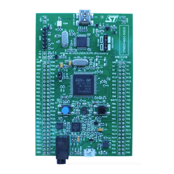
The STM32F401 Discovery kit (32F401CDISCOVERY) helps you to discover the entry level
of the STM32F4 series and to develop your applications. It is based on an
STM32F401VCT6 and includes an ST-LINK/V2 embedded debug tool interface, ST MEMS
Gyroscope, ST MEMS accelerometer + magnetometer, ST MEMS digital microphone, audio
DAC with integrated class D speaker driver, LEDs, pushbuttons and a USB OTG micro-AB
connector.
Figure 1. STM32F401 Discovery board
September 2013
DocID025174 Rev 1
1/39
www.st.com
Advertisement
Table of Contents

Related Manuals for ST STM32F401


Summary of Contents for ST STM32F401
-
Page 1: Figure 1. Stm32F401 Discovery Board
Discovery kit for STM32F401 line Introduction The STM32F401 Discovery kit (32F401CDISCOVERY) helps you to discover the entry level of the STM32F4 series and to develop your applications. It is based on an STM32F401VCT6 and includes an ST-LINK/V2 embedded debug tool interface, ST MEMS... -
Page 2: Table Of Contents
Embedded ST-LINK/V2 ........ - Page 3 UM1669 Contents Revision history ......... . . 37 DocID025174 Rev 1 3/39...
- Page 4 List of tables UM1669 List of tables Table 1. ON/OFF conventions ............6 Table 2.
- Page 5 Figure 7. STM32F401 Discovery board connections image ....... 16 Figure 8.
-
Page 6: Conventions
Conventions UM1669 Conventions Table 1 provides the definition of some conventions used in the present document. Table 1. ON/OFF conventions Convention Definition Jumper JPx ON Jumper fitted Jumper JPx OFF Jumper not fitted Solder bridge SBx ON SBx connections closed by solder Solder bridge SBx OFF SBx connections left open 6/39... -
Page 7: Quick Start
Ensure that the jumpers JP2 and CN3 are set to "on" (Discovery mode). Connect the STM32F401 Discovery board to a PC using a USB cable type A/mini-B through the USB ST-LINK connector CN1, to power the board. The LED LD2 (PWR) will light up and the four LEDs between the buttons B1 and B2 start blinking. -
Page 8: Features
STM32F401VCT6 microcontroller featuring 256 KB of Flash memory, 64 KB of RAM in an LQFP100 package • On-board ST-LINK/V2 with selection mode switch to use the kit as a standalone ST- LINK/V2 (with SWD connector for programming and debugging) •... -
Page 9: Hardware Layout
UM1669 Hardware layout Hardware layout The STM32F401 Discovery board has been designed around the STM32F401VCT6 microcontroller in a 100-pin LQFP package. Figure 1 illustrates the connections between the STM32F401VCT6 and its peripherals (ST- LINK/V2, pushbutton, LED, Audio DAC, USB, ST MEMS gyroscope, ST MEMS accelerometer + magnetometer, ST MEMS microphone, and connectors). -
Page 10: Figure 2. Top Layout
Hardware layout UM1669 Figure 2. Top layout ST-LINK/V2 ST-LINK/V2 LD2 (red LED) LD1 (red/green LED) SWD connector ST-LINK/DISCOVERY selector 5 V power supply input/output 3 V power supply output measurement SB1 (B2-RESET) STM32F401VCT6 LD3 (orange LED) B2 reset button B1 user button... -
Page 11: Figure 3. Bottom Layout
UM1669 Hardware layout Figure 3. Bottom layout SB2, SB4, SB6, SB8 (RESERVED) SB3, SB5, SB7, SB9 (DEFAULT) SB10, SB11 (RX, TX) SB15 (SWO) SB16 (X2 crystal) SB17 (X3 crystal) SB12 (STM_RST) SB13 (NRST) SB18 (X3 crystal) SB14 (X2 crystal) SB19 (BOOT0) SB20 (BOOT1) SB21 (B1-USER) MS32362V1... -
Page 12: Stm32F401Vct6 Microcontroller
Hardware layout UM1669 STM32F401VCT6 microcontroller This ARM Cortex-M4 32-bit MCU with FPU has 105 DMIPS, up to 256 KB Flash/64 KB RAM, USB OTG FS, 10 TIMs, 1 ADC, 11 comm. interfaces. Figure 4. STM32F401VCT6 microcontroller STM32F401VCT6 256 Kbytes of Flash memory 64 Kbytes of RAM LQFP100 14 x 14 mm MS32365V1... - Page 13 – Up to 10 timers: 16 and 32 bits running up to 84 MHz High integration Smaller board space allowing for smaller applications – WLCSP49 3 x 3 mm (STM32F401, 256-Kbyte Flash/ 64-Kbyte SRAM) Extensive tools and software solutions – Hardware sector protection with execute only access –...
-
Page 14: Figure 5. Stm32F401Vct6 Block Diagram
Hardware layout UM1669 Figure 5. STM32F401VCT6 block diagram NJTRST, JTDI, JTCK/SWCLK JTAG & SW JTDO/SWD, JTDO NVIC TRACECLK D-BUS TRACED[3:0] ARM Cortex-M4 84 MHz I-BUS Flash S-BUS up to 256 KB SRAM 64 KB 8 Streams DMA2 AHB2 84 MHz FIFO OTG FS ID, VBUS, SOF... -
Page 15: Embedded St-Link/V2
UM1669 Hardware layout Embedded ST-LINK/V2 The ST-LINK/V2 programming and debugging tool is integrated on the STM32F401 Discovery board. The embedded ST-LINK/V2 can be used in 2 different ways according to the jumper states (see Table • Program/debug the MCU on board, •... -
Page 16: Using St-Link/V2 To Program/Debug The Stm32F401 On Board
4.2.1 Using ST-LINK/V2 to program/debug the STM32F401 on board To program the STM32F401 on board, simply plug in the two jumpers on CN3, as shown in Figure 7 in red, but do not use the CN2 connector as that could disturb communication with the STM32F401VCT6 of the STM32F401 Discovery board. -
Page 17: Using St-Link/V2 To Program/Debug An External Stm32 Application
Hardware layout 4.2.2 Using ST-LINK/V2 to program/debug an external STM32 application It is very easy to use the ST-LINK/V2 to program the STM32 on an external application. Simply remove the 2 jumpers from CN3 as shown in Figure 8, and connect your application... -
Page 18: Power Supply And Power Selection
5 V can also be used as input power supplies, e.g. when the USB connector is not connected to the PC. In this case, the STM32F401 Discovery board must be powered by a power supply unit or by an auxiliary equipment complying with standard EN-60950-1: 2006+A11/2009, and must be Safety Extra Low Voltage (SELV) with limited power capability. -
Page 19: On Board Audio Capability
CS43L22 USB OTG supported The STM32F401 is used to drive only USB OTG full speed on this board. The USB micro- AB connector (CN5) allows the user to connect a host or device component, such as a USB key, mouse, and so on. -
Page 20: Jp2 (Idd)
If PH0 and PH1 are only used as GPIOs instead of as a clock, then SB14 and SB16 are closed and R24, R25 and R66 are removed. MCO from ST-LINK (from MCO of the STM32F103) This frequency cannot be changed, it is fixed at 8 MHz and connected to PH0-OSC_IN of the STM32F401VCT6. -
Page 21: Solder Bridges
Reserved, do not modify SB10,11 (RX,TX) Reserved, do not modify No incidence on STM32F103C8T6 (ST-LINK/V2) NRST signal SB12 (STM_RST) STM32F103C8T6 (ST-LINK/V2) NRST signal is connected to GND Ω BOOT0 signal of the STM32F401VCT6 MCU is held low through a 510 pull- down resistor SB19 (BOOT0) Ω... -
Page 22: Extension Connectors
4.13 Extension connectors The male headers P1 and P2 can connect the STM32F401 Discovery board to a standard prototyping/wrapping board. STM32F401VCT6 GPI/Os are available on these connectors. P1 and P2 can also be probed by an oscilloscope, logical analyzer or voltmeter. - Page 23 UM1669 Hardware layout Table 6. MCU pin description versus board function (page 2 of 8) MCU pin Board function Main Alternate function functions TIM1_CH1N, TIM3_CH2, SPI1_MOSI, ADC1_7 MCO_1, TIM1_CH1, I2C3_SCL, USART1_CK, USB_FS_SOF TIM1_CH2, I2C3_SMBAL, USART1_TX, USB_FS_VBUS TIM1_CH3, PA10 USART1_RX, USB_FS_ID TIM1_CH4, USART1_CTS, PA11...
- Page 24 Hardware layout UM1669 Table 6. MCU pin description versus board function (page 3 of 8) MCU pin Board function Main Alternate function functions TIM1_CH3N, TIM3_CH4, ADC1_9 JTDO-SWO, TIM2_CH2, SPI1_SCK, SPI3_SCK/I2S3_CK, I2C2_SDA JTRST, TIM3_CH1, SPI1_MISO, SPI3_MISO, I2S3ext_SD, I2C3_SDA TIM3_CH2, I2C1_SMBAL, SPI1_MOSI, SPI3_MOSI/I2S3_SD TIM4_CH1, I2C1_SCL, USART1_TX,...
- Page 25 UM1669 Hardware layout Table 6. MCU pin description versus board function (page 4 of 8) MCU pin Board function Main Alternate function functions TIM1_BKIN, I2C2_SMBAL, PB12 SPI2_NSS/I2S2_WS, I2S2ext_WS TIM1_CH1N, PB13 SPI2_SCK/I2S2_CK, I2S2ext_CK TIM1_CH2N, PB14 SPI2_MISO, I2S2ext_SD RTC_50Hz, TIM1_CH3N, PB15 SPI2_MOSI/I2S2_SD, I2S2ext_MISO ADC1_10 ADC1_11...
- Page 26 Hardware layout UM1669 Table 6. MCU pin description versus board function (page 5 of 8) MCU pin Board function Main Alternate function functions MCO_2, TIM3_CH4, I2C3_SDA, I2S2_CKIN, SDIO_D1 I2S3ext_CK, PC10 SPI3_SCK/I2S3_CK, SDIO_D2 I2S3ext_SD, PC11 SPI3_MISO, SDIO_D3 I2S3ext_MISO, PC12 SPI3_MOSI/I2S3_SD, SDIO_CK PC13 TAMP_1 PC14...
- Page 27 UM1669 Hardware layout Table 6. MCU pin description versus board function (page 6 of 8) MCU pin Board function Main Alternate function functions USART2_CK PD10 PD11 PD12 TIM4_CH1 PD13 TIM4_CH2 PD14 TIM4_CH3 PD15 TIM4_CH4 TIM4_ETR TRACECLK, SPI4_SCK TRACED0 TRACED1, SPI4_NSS TRACED2, TIM9_CH1, SPI4_MISO TRACED3, TIM9_CH2,...
- Page 28 Hardware layout UM1669 Table 6. MCU pin description versus board function (page 7 of 8) MCU pin Board function Main Alternate function functions TIM1_CH1N TIM1_CH1 PE10 TIM1_CH2N PE11 TIM1_CH2, SPI4_NSS TIM1_CH3N, PE12 SPI4_SCK PE13 TIM1_CH3, SPI4_MISO 44 PE14 TIM1_CH4, SPI4_MOSI 45 PE15 TIM1_BKIN OSC_IN...
- Page 29 UM1669 Hardware layout Table 6. MCU pin description versus board function (page 8 of 8) MCU pin Board function Main Alternate function functions DocID025174 Rev 1 29/39...
-
Page 30: Mechanical Drawing
Mechanical drawing UM1669 Mechanical drawing Figure 9. STM32F401 Discovery board mechanical drawing 30/39 DocID025174 Rev 1... -
Page 31: Electrical Schematics
UM1669 Electrical schematics Electrical schematics Figure 10. STM32F401 Discovery board DocID025174 Rev 1 31/39... -
Page 32: Figure 11. St-Link/V2 (Swd Only)
Electrical schematics UM1669 Figure 11. ST-LINK/V2 (SWD only) 32/39 DocID025174 Rev 1... -
Page 33: Figure 12. Stm32F401Vct6 Mcu
UM1669 Electrical schematics Figure 12. STM32F401VCT6 MCU DocID025174 Rev 1 33/39... -
Page 34: Figure 13. Audio
Electrical schematics UM1669 Figure 13. Audio 34/39 DocID025174 Rev 1... -
Page 35: Figure 14. Usb_Otg_Fs
UM1669 Electrical schematics Figure 14. USB_OTG_FS DocID025174 Rev 1 35/39... -
Page 36: Figure 15. Peripherals
Electrical schematics UM1669 Figure 15. Peripherals 36/39 DocID025174 Rev 1... -
Page 37: Table 7. Document Revision History
UM1669 Revision history Revision history Table 7. Document revision history Date Revision Changes 10-Sep-2013 Initial release. DocID025174 Rev 1 37/39... - Page 38 No license, express or implied, by estoppel or otherwise, to any intellectual property rights is granted under this document. If any part of this document refers to any third party products or services it shall not be deemed a license grant by ST for the use of such third party products or services, or any intellectual property contained therein or considered as a warranty covering the use in any manner whatsoever of such third party products or services or any intellectual property contained therein.
Need help?
Do you have a question about the STM32F401 and is the answer not in the manual?
Questions and answers