Table of Contents
Advertisement
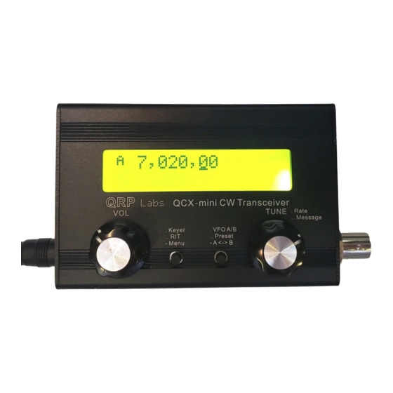
QCX-mini CW
Transceiver
QCX-mini 5W CW Transceiver kit assembly instructions
The "QCX-mini": a single band, high performance 5W
CW Transceiver with built-in alignment and test
equipment, iambic keyer, WSPR beacon mode, and
more...
Designed and produced by QRP Labs, 2017-2020
pictured with:
Palm Radio pico paddle
http://palm-radio.de
and the XYL's old iPhone's earbuds
1
QCX-mini assembly Rev 1.05
Advertisement
Table of Contents

Related Manuals for QRP Labs QCX-mini CW


Summary of Contents for QRP Labs QCX-mini CW
- Page 1 The “QCX-mini”: a single band, high performance 5W CW Transceiver with built-in alignment and test equipment, iambic keyer, WSPR beacon mode, and more... Designed and produced by QRP Labs, 2017-2020 pictured with: Palm Radio pico paddle http://palm-radio.de and the XYL’s old iPhone’s earbuds...
-
Page 2: Table Of Contents
Contents 1. Introduction..............................4 2. Parts list................................5 3. Assembly – general guidelines........................10 3.1 Inventory parts............................22 3.2 Wind and install transformer T1......................23 3.3 Install IC2 socket.............................30 3.4 Install 100nF (0.1uF, “104”) capacitors....................31 3.5 Install all 470nF, “474” capacitors......................32 3.6 Install 47nF, “473” capacitor........................32 3.7 Install capacitors C25 and C26 from Low Pass Filter kit................33 3.8 Install capacitors C27 and C28 from Low Pass Filter kit................34 3.9 Install capacitor C30..........................35... - Page 3 3.47 Installation in the optional QCX-mini enclosure...................78 3.48 QCX-mini GPS interface and PTT output....................81 3.49 QCX-mini CAT port..........................82 4. Circuit design of the QCX-mini........................83 4.1 Block diagram and summary........................83 4.2 Circuit diagram............................83 4.3 Synthesized oscillator..........................86 4.4 Transmit/Receive switch.........................87 4.5 Band Pass, Phase Splitter, QSD and pre-amps..................88 4.6 90-degree audio phase shift........................89 4.7 CW filter..............................90 4.8 Audio amplifier............................90...
-
Page 4: Introduction
1. Introduction Thank you for purchasing this high performance single-band 5W CW transceiver kit, the QCX-mini (for QRP Labs CW Xcvr mini). This kit has a long list of features! Special portable-friendly features: Small size: 95 x 63 x 25mm enclosure (plus protrusions) •... -
Page 5: Parts List
Please make use of troubleshooting resources at if you have http://qrp-labs.com/qcxmini any problems. If you need further help, join the QRP Labs discussion forum on groups.io and post a message about your problem. 2. Parts list Many components are SMD, pre-soldered to the PCB in the factory. Only through-hole components need to be installed by the constructor. - Page 6 Value Description Component numbers Linear potentiometer R36 (on controls board) Trimmer R47 (on display board) potentiometer Capacitors (50V, Multi-layer Ceramic capacitors) Value Description Component numbers C14, 16, 18, 23, 33 2.2nF C19, 20 3.3nF 10nF C4, 7, 10, 42 33nF 39nF 47nF Label “473”...
- Page 7 60m (C30 is two capacitors in parallel) Value Description Component numbers 39pF Label “390” 22pF Label “220” 30pF Label “300” C30 (C30 is two capacitors in parallel) 56pF Label “560” C30 (C30 is two capacitors in parallel) 680pF Label “681" C27, 28 1200pF Label “122”...
- Page 8 Description Component numbers SMD: Si5351A, 10-pin MSOP IC1 ATmega328, microcontroller SMD: 74ACT00N SMD: FST3253 SMD: LM4562 dual op-amp SMD: OPA2277 dual op-amp IC6-10 SMD: AMS1117-5.0, 5V IC11 SMD: BSS123 MOSFET Q4, 5, 7, 100 (Q100 on display board) BS170: TO92 MOSFET Q1-3 MPS751 TO92 transistor Inductors...
- Page 9 Value Description Component numbers 1.4uH 21 turns on T37-6 core (yellow) L1, L3 1.7uH 24 turns on T37-6 core (yellow) 1.0uH 16 turns on T37-2 core (red) 5+5+5+38 turns, T50-2 core (red) Value Description Component numbers 1.1uH 19 turns on T37-6 core (yellow) L1, L3 1.3uH 20 turns on T37-6 core (yellow)
-
Page 10: Assembly - General Guidelines
Value Description Component numbers Rotary encoder with shaft button 1602 HD44780 LCD 1602, yellow/green back-light 20MHz HC49/4H quartz crystal XTAL1 27MHz HC49/4H quartz crystal XTAL2 Main PCB Display PCB panel Knob Knob to fit rotary encoder and R36 200cm 0.33mm diameter wire (AWG #28) M3 10mm Steel 10mm long M3 screw Steel M3 nut... - Page 11 I recommend just install everything then power As per standard QRP Labs practice, the ATmega328P microcontroller has a 28-pin DIP socket in case you may wish to subsequently replace it for firmware upgrades etc. Many of the components in this kit are in surface mount packages (SMD) and these are already soldered to the PCB for you, at the factory.
- Page 12 The QCX-mini kit is very compact. It requires a higher degree of precision than many other QRP Labs kits, if you are intending to install it in the optional enclosure. It’s not more difficult. It just requires a bit more care. Pay careful attention to the following points, throughout the assembly.
- Page 13 4. Component lead offcuts In this kit, you must KEEP all the component lead off-cuts! Yes, I know, it’s fun when you cut them with the wire-cutter to hear them pinging around the room somewhere, and even more fun when your XYL finds them embedded in the carpet somewhere else in the house, and nothing quite beats the entertainment value of when she steps on one and it is embedded in the...
- Page 14 The following diagrams show the PCB layout and track diagrams of the display and main PCBs of the QCX-mini kit (red track = top side; blue track = bottom side; there are no hidden layers). QCX-mini assembly Rev 1.05...
- Page 15 QCX-mini assembly Rev 1.05...
- Page 16 QCX-mini assembly Rev 1.05...
- Page 17 QCX-mini assembly Rev 1.05...
- Page 18 Tracks shown in BLUE are on the bottom layer. Tracks shown in RED are on the top layer. There are only two layers (nothing is hidden in the middle). Not shown in this diagram are the extensive ground-planes, on both sides of the board. Practically everything on both layers that isn’t a RED or BLUE track, is ground-plane! The two ground-planes are connected at frequent intervals (not more than 0.1-inches) by vias.
- Page 19 Main board: Display board: Controls board: QCX-mini assembly Rev 1.05...
- Page 20 PCB. The conversion is supported by the uSDX group https://groups.io/g/ucx and there is no technical support from QRP Labs. The daughtercard is supplied as-is, to assist this conversion for experimenters who wish to try uSDX.
- Page 21 The PCBs may come with a surplus strip of It’s also important to gently file away any material along one or more edges; this is rough edges of the PCB from where it has used during the manufacturing processes to been snapped out of the larger panel.
-
Page 22: Inventory Parts
Inventory parts Refer to parts list in section 2. The following photographs are to aid component identification. Several components are missing from this photo. So for a complete inventory refer to the parts list, remembering to check the band-specific components for your band. Remember that the main kit bag contains several smaller clear plastic zip-lock bags, and components are spread through the different bags with no apparent rules or reason. -
Page 23: Wind And Install Transformer T1
Wind and install transformer T1 This is the only really tricky piece of the assembly: the receiver input transformer T1. Follow these instructions carefully, it is tricky but quite feasible if you go step by step. This is the FIRST step because it is easiest to do the installation when there are no other components nearby. - Page 24 QCX-mini assembly Rev 1.05...
- Page 25 The number of turns in each winding depends on the band you are building the kit for. Refer to the following table. For convenience, the remainder of the instructions in this section refer to the 40m version (38 + 5 + 5 + 5 turns). But MAKE SURE you wind the correct number of turns for your band! Band Primary...
- Page 26 In all cases, there is one long secondary winding, and three other short identical windings. To make things easier, we will wind all windings together in one go, this will guarantee that the “sense” of each winding will be the same. At the intended breaks between the windings, we will leave large loops of wire, that we can later cut one by one to make sure the wires go in the correct holes.
- Page 27 7) Do the same thing for two more loops, which are between the 43rd and 44th turns, and 48th and 49th turns respectively. It is easy to lose count. An easy way is after step 6, pass the wire through the hole 5 more times, and on the 5th one, make a loop.
- Page 28 12)Next cut the 2nd loop, and un-twist the twisted section near the toroid body. 13)Similar to step 11; the wire which came over the toroid body has five turns then goes into hole 4, which you did in step 11. Insert this wire-end into hole 3. The other wire end that came from under the toroid body should be gently pushed toward the toroid, and pulled up through the center hole of the toroid.
- Page 29 17)Now you can solder the eight connections under the PCB. I recommend doing one pair of wires at a time; this way, the other wires will hold the toroid in place and stop it falling out. Start with the two un-twisted wires. Pull each wire tight, bend it over at about 45-degrees, and cut it 1-2mm away from the PCB surface.
-
Page 30: Install Ic2 Socket
Install IC2 socket PUSH IT UP TOWARDS THE TOP OF THE BOARD, TO MAKE MORE SPACE FOR THE TCXO PCB Install the 28-pin IC socket for IC2. Take care to match the dimple on the socket, with the dimple on the PCB silkscreen. It is critical to insert the microcontroller with the correct orientation. -
Page 31: Install 100Nf (0.1Uf, "104") Capacitors
Install 100nF (0.1uF, “104”) capacitors There are two 100nF (0.1uF) capacitors, these have the code “104” written on them. Be sure to identify the correct capacitors, using a magnifying glass or jeweler's loupe. These capacitors are C12 and C29. Place each in the correct position on the board, and slightly bend the legs outwards at about 30-degrees angle so that they stay in place. -
Page 32: Install All 470Nf, "474" Capacitors
Install all 470nF, “474” capacitors The five 470nF capacitors are labeled “474”, and are capacitors C11, C43, C44, C45 and C46. Install 47nF, “473” capacitor The 47nF (0.047uF) capacitor is labeled “473” and is capacitor C9. QCX-mini assembly Rev 1.05... -
Page 33: Install Capacitors C25 And C26 From Low Pass Filter Kit
Install capacitors C25 and C26 from Low Pass Filter kit The value of these capacitors depends on your chosen band. The capacitors are located inside the separate Low Pass Filter bag in your main kit bag. Refer to the following table to find the correct capacitor value for your band: Band Value... -
Page 34: Install Capacitors C27 And C28 From Low Pass Filter Kit
Install capacitors C27 and C28 from Low Pass Filter kit The value of these capacitors depends on your chosen band. The capacitors are located inside the separate Low Pass Filter bag in your main kit bag. Refer to the following table to find the correct capacitor value for your band: Band Value... -
Page 35: Install Capacitor C30
Install capacitor C30 This capacitor is band dependent. The kit contains all required capacitor values for all bands. Install the one appropriate to your band. Refer to the following table to find the correct capacitor value for your band Band Value Label 180pF... -
Page 36: Install Capacitors C5 And C8
3.10 Install capacitors C5 and C8 These capacitors are band dependent. They add parallel capacitance to trimmer capacitor C1 to bring it to the required value. The kit contains all required capacitor values. Install the capacitor(s) appropriate to your band. Refer to the following table to find the correct capacitor value(s) for your band. -
Page 37: Install 1Uf, "105" Capacitors C21, And C22
3.11 Install 1uF, “105” capacitors C21, and C22 There are two 1uF capacitors labeled “105”, which are C21 and C22. QCX-mini assembly Rev 1.05... -
Page 38: Install 1N5819 Diode
3.12 Install 1N5819 diode This diode D33 is the diode with a black body, and a white stripe. It is installed vertically. It must be orientated correctly, with the white stripe on the diode matching the white stripe on the PCB. This diode protects the radio against reverse polarity. -
Page 39: Install 20Mhz Crystal Xtal1
3.13 Install 20MHz crystal XTAL1 The engraving on this crystal is “20.000” or “CE20.000”. QCX-mini assembly Rev 1.05... -
Page 40: Install 27Mhz Crystal Xtal2 Or Tcxo Option
3.14 Install 27MHz crystal XTAL2 or TCXO option If you are going to install the 27MHz crystal, do so now. The engraving on this crystal is “27.000”. If you are going to install the 25MHz TCXO, skip this diagram and refer to the following instructions. - Page 41 Install the TCXO module as follows: Find a suitable file. File the rough edges of the TCXO module flat Solder wire off-cuts into the holes shown, Thread the TCXO module carefully onto the and cut any excess wire on the underside of wires.
-
Page 42: Install 500-Ohm Multi-Turn Trimmer Potentiometer
Note that when using the TCXO module, the reference frequency setting must be 25,000,000 MHz, not the default which is 27,004,000 MHz. This is further described in the initial set-up instructions, below. This is because the QCX-mini can operate either with 25MHz reference (the TCXO module) or with 27MHz (the supplied crystal), BUT, you have to tell it which one you have installed! 3.15 Install 500-ohm multi-turn trimmer potentiometer... -
Page 43: Install 50K Multi-Turn Trimmer Potentiometers
3.16 Install 50K multi-turn trimmer potentiometers There are two 50K multi- turn trimmer potentiometers, R17 and R24. They are the small blue box components with label “’503”. The trimmer potentiometers must be prepared before installation by cutting off the small plastic ledges with a wire- cutter, as described in the preceding section. -
Page 44: Install 470Uf Capacitors
3.17 Install 470uF capacitors There are two 470uF capacitors in the kit: C24, C47. These are polarized electrolytic capacitors and MUST be installed with the correct orientation! The capacitor NEGATIVE wire must be installed in the hole indicated on the PCB silkscreen and the layout diagram by the solid black bar;... -
Page 45: Install 30Pf Trimmer Capacitor C1
3.18 Install 30pF trimmer capacitor C1 Insert the component pins carefully and with the correct orientation which matches the PCB. Cut the small pin stubs on the underside (solder side) of the PCB, they only protrude a few mm but when installed in the enclosure could be rather close to the aluminium floor. QCX-mini assembly Rev 1.05... -
Page 46: Install Mps751 Transistor Q6
3.19 Install MPS751 transistor Q6 Be careful to correctly identify this transistor by its markings, as the package style is similar to the other transistors. Carefully bend and insert the wires so that the transistor’s flat side is flat flush against the PCB surface, and the body of the transistor is aligned with the square on the layout diagram... -
Page 47: Install Three Bs170 Transistors
3.20 Install three BS170 transistors The remaining three transistors in the kit are BS170 MOSFETs: Q1, Q2 and Q3 For Q1, Q2 and Q3, carefully follow the same installation procedure as the previous section, making sure that the transistors are neatly aligned in the correct positions near the hole in the PCB. -
Page 48: Install 2X3-Pin In-Circuit Programming Header
3.21 Install 2x3-pin in-circuit programming header This male pin header can be used to connect an AVR Programmer to apply firmware updates if desired. Insert the SHORT end of the pins into the PCB. Solder one pin in place first and check that the header is nicely seated on the PCB before soldering the other 5. QCX-mini assembly Rev 1.05... -
Page 49: Install 2X5 Lcd Header
3.22 Install 2x5 LCD header This female pin header (socket) connects the main QCX-mini PCB to the display board above it. Solder one pin in place first and check that the header is nicely seated on the PCB before soldering the other 9. Be sure to install the 2x5-pin FEMALE pin header connector (see right), not the male header connector which is installed on the LCD board. -
Page 50: Install 2X4 Ui Header
3.23 Install 2x4 UI header This female pin header (socket) connects the main QCX-mini PCB to the controls board above it. Solder one pin in place first and check that the header is nicely seated on the PCB before soldering the other 8. 3.24 Wind and install toroid L4 L4 is type T37-2. - Page 51 This is the number 1 cause of problems with QRP Labs kit construction: failure to remove the wire enamel. One method of removing the wire enamel is to scrape it off at the ends, either with sandpaper, or carefully scratching with a knife or wire cutters. However, my favourite method is just to burn off the enamel.
-
Page 52: Wind And Install Toroid L2
3.25 Wind and install toroid L2 L2 is a small toroid ring painted yellow or red on one side. It is part of the supplied Low Pass Filter kit bag. Installation of the inductor is similar to the previous section. Remember to remove the wire enamel and check! In the QCX-mini kit, there is some advantage to winding the toroid with the turns... -
Page 53: Wind And Install Toroids L1 And L3
3.26 Wind and install toroids L1 and L3 L1 and L3 are small toroid rings painted yellow or red on one side. They are part of the supplied Low Pass Filter kit bag. Installation of the inductors is similar to the previous section. -
Page 54: Install 2.1Mm Power Connector
3.27 Install 2.1mm power connector Install the 2.1mm power connector, orientated to match the PCB silkscreen. It is important to install this accurately so that if you install the QCX-mini in the optional aluminium enclosure, the connector is correctly aligned with the associated panel hole. QCX-mini assembly Rev 1.05... -
Page 55: Install Rf Output Bnc Connector
Accurate alignment is very important, to ensure that the connector fits into the hole of the optional QRP Labs QCX-mini enclosure (if used). The rim on the connector body should not overlap the edge of the PCB. The BNC connector must sit squarely on the board with the metal body extending at 90-degrees to the PCB edge. -
Page 56: Install 3.5Mm Stereo Jack Connectors
This is the final step in the assembly of the main board. There are four stereo 3.5mm jack connectors, used for the audio output (earphones), optional connection of a paddle, optional CAT connection, and optional PTT output to 50W PA kit (optional QRP Labs kit). Accurate alignment is very important, to ensure that the connectors fit into the holes of the optional QRP Labs QCX-mini enclosure (if used). -
Page 57: Break Apart Inner Pcbs Of Display Board
3.30 Break apart inner PCBs of display board Now that the main PCB assembly is complete, the display board and controls board are assembled next. The display board panel contains several smaller PCBs which are joined to the display board via thin PCB bridges which have a line of holes, designed to be easily snapped out. Controls PCB: this will hold the gain control, rotary encoder (tuning) control and the •... - Page 58 Squeeze and twist the PCB bridge to snap Location of five small PCBs to snap out of out using pliers or wire cutter the display board panel Gently grip and bend to remove – but be File rough edges of the cut-outs in the panel careful of the central spar of the panel PCB PCB and the broken-out pieces All five parts after careful filing...
-
Page 59: Install Lcd Module
3.31 Install LCD module Precision assembly is essential – follow the guide below carefully. Identify the pairs of M3 6mm screws and Fit the LCD module from behind the PCB, nuts. They may be nylon or metal. with its body through the rectangular cut-out Bolt the LCD module, ensuring equal gaps Drop component off-cuts through the 16 at top and bottom;... -
Page 60: Install 2X5-Pin Male Pin Header Connector
3.32 Install 2x5-pin male pin header connector Install the 2x5-pin male header from below the display PCB; the short-end of the pins should be inserted through the PCB from the bottom side, as shown. Solder one pin first, and check alignment before continuing with the other nine. Try to ensure that the pin header sits squarely and centrally in its allocated position. -
Page 61: Install 20K Trimmer Potentiometer R47
3.34 Install 20K trimmer potentiometer R47 The 20K single-turn trimmer potentiometer allows adjustment of the LCD contrast. This potentiometer, similar to the 24-turn trimmer potentiometers installed on the main QCX-mini PCB, has four little feet, one in each corner. Unfortunately these make the trimmer too high and it may prevent the PCB from sliding into the QCX-mini enclosure later. -
Page 62: Install 2X4-Pin Male Header On Controls Pcb
3.35 Install 2x4-pin male header on controls PCB Next comes the assembly of the controls PCB, which holds the gain control, rotary encoder (frequency tuning), and the two tactile switch buttons. The 2x4-pin header must be installed with the small spacer PCB sandwiched between the connector body and the underside of the PCB. -
Page 63: Install Rotary Encoder
3.36 Install rotary encoder The rotary encoder is installed in the large hole labeled SW1 on the controls PCB. First cut off two large PCB-mounting lugs as Position a flat-headed screwdriver above shown using wire-cutters. Do NOT cut pins. one of the five switch pins. Bend over the pin through 180-degrees so Repeat the same procedure for the four that it points to the front of the control. -
Page 64: Install Tactile Switch Buttons
Solder each of the five switch pins, on the underside of the PCB (the side with the blue body of the rotary encoder). The center pin of the three may benefit from a piece of wire off-cut to extend it to reach the PCB hole. 3.37 Install tactile switch buttons The two buttons should be installed on the control PCB as shown. -
Page 65: Install 11Mm Nylon Hex Spacer
Install component off-cut wires, soldering Trim any excess length of both the pins, and first the PCB end then the potentiometer pin the off-cut component wires. It is important end; make the connection as close to the to trim these as close to the joint as possible green potentiometer body as possible. -
Page 66: Fit Controls Pcb To Main Pcb
3.40 Fit Controls PCB to main PCB Now fit the Controls PCB to the main PCB by plugging together the two 2x4-pin header connectors. Fit an M3 6mm screw from the underside of the main PCB, screwed into the 11mm nylon hex spacer pillar that is fixed to the Controls PCB, as shown in the following photograph. -
Page 67: Install Microcontroller
3.41 Install microcontroller Install IC2, the programmed ATmega328P microcontroller, in the 28-pin DIP socket on the main QCX-mini PCB. Be very careful to ensure that the dimple on the chip is aligned with the dimple on the 28- pin DIP socket, which itself should already be aligned with the dimple on the PCB silkscreen. - Page 68 If it’s Tantalum: Any > 10uF, 16V. Straighten the wires using needle-nose Identify – and + wires (polarity is critical). pliers or something Positive is long wire, and + label on body Cut negative wire to 5mm; tin the wire and The capacitor should be face (label) side the left pin of the voltage regulator.
- Page 69 Electrolytic: Any small capacitor rated > Cut the negative wire to approx 6mm. This 10uF, 16V. wire will be soldered to the left-hand terminal Identify – and + wires (polarity is critical). of the AMS1117-5.0 voltage regulator Diameter max 5mm, length max 9mm. Tin the negative wire of the capacitor with a Put the capacitor lying horizontally in small blob of solder, which will make it...
-
Page 70: Plug Together The Two Boards
3.43 Plug together the two boards Now you can carefully plug together the two circuit boards. The best way to do this is to concentrate on getting the 5-pin headers at the top left of the PCBs, to mate accurately with each other. -
Page 71: Notes On Fault-Finding For The Qcx-Mini
If you want to use a small loudspeaker you will need to ensure this is an “amplified speaker” because the audio output will not be strong enough to drive a speaker directly. 3) Antenna system The RF output is a filtered 50-ohm BNC output for connection to a usual antenna system (antenna, and matching unit if applicable). -
Page 72: Adjustment And Alignment
13.8V supply (normally nearer to 6W). https://groups.io/g/qrplabs is the QRP Labs discussion forum and is full of very helpful people who will be able to advise. Be sure to describe your problem as fully as possible since without this, any faults will be impossible to diagnose. - Page 73 Unplug the antenna during alignment of the radio! Connect a 50-ohm dummy load such as the QRP Labs dummy load kit http://qrp-labs.com/dummy When using the TCXO module option, change menu item 8.5 Ref frq to 25,000,000. It is critical to this before any further alignment.
- Page 74 First adjust the band-pass trimmer capacitor C1. To do this, give one long press to the “Select” (left) button. The screen now displays the first menu category: 1 Preset Turn the rotary encoder until you see the alignment menu: 8 Alignment Now press the “Select”...
- Page 75 this photograph, 27 little vertical bars are shown, which means the actual measured amplitude value is 13,824. If the displayed bar drops below one third of the width of the LCD, then the division factor is reduced by one and the bar is re-displayed. On the other hand, if the displayed bar overflows the right edge of the screen, the division factor is increased by one.
- Page 76 20MHz system clock oscillator of the microcontroller. These adjustments can be made manually, or by connection of a GPS module such as the QRP Labs QLG1 GPS receiver kit. However, since this calibration is a lot less urgent than QCX-mini assembly Rev 1.05...
- Page 77 the Band Pass Filter peaking and unwanted sideband cancellation, they are left until the description of these menu items in the operating manual. Following the adjustment of these alignment trimmers, the radio is ready to use. A lot of settings are available in the configuration menu, and you should read the operation manual to understand and make use of all the features! You may now bolt the two PCBs together by screwing the four M3 6mm nylon screws into the 11mm spacers which hold the two PCBs at the correct separation;...
-
Page 78: Installation In The Optional Qcx-Mini Enclosure
3.47 Installation in the optional QCX-mini enclosure Installation in the QCX-mini enclosure is simple and requires no wiring. It is important to do the assembly in the correct sequence, as follows. Start with the Display board… … and the main board, with the controls board bolted in position. - Page 79 Place the front of the enclosure face down Align the 2x5-pin header connector between on the bench as shown, and prepare to the main and display boards; some wriggling attach the main board. will be needed to get the controls to fit through the holes in the front panel.
- Page 80 Screw in the other four black screws in the Apply the supplied four self-adhesive feet to corners of the right-hand side panel. suitable positions on the base of the enclosure if desired (optional). Install the supplied knobs by tightening their grub screws.
-
Page 81: Qcx-Mini Gps Interface And Ptt Output
The GPS produces two output signals, PPS (Pulse-per-second) and RxD (Serial data), in addition to ground. Optionally +5V may also be connected, in order to power the GPS module. A GPS such as the QRP Labs QLG1 is perfect for this see http://qrp-labs.com/qlg1 The GPS signals (PPS and RxD) use the same microcontroller pins as the paddle Dah and Dit respectively. -
Page 82: Qcx-Mini Cat Port
The following diagram shows the connections. PTT output The PTT output is at the ring of the 5V/PTT connector jack. This signal is 0V when the QCX-mini is in Receive mode, and +5V when the QCX-mini is in Transmit mode. If you are connecting the QCX-mini to the companion 50W PA kit, then this signal has to be connected to the 50W PA kit to cause it to switch to Transmit mode. -
Page 83: Circuit Design Of The Qcx-Mini
4. Circuit design of the QCX-mini Block diagram and summary This CW transceiver is a high performance, yet simple and low cost, analogue design. The transmitter uses a high efficiency Class-E amplifier which results in low current draw on transmit, and inexpensive transistors with little or no heatsinks. The receiver is a direct conversion type utilizing the famous high performance Quadrature Sampling Detector, also known sometimes as the “Tayloe Detector”... - Page 84 QCX-mini assembly Rev 1.05...
- Page 85 The circuit diagram (schematic) of the main PCB is shown on the previous page. The circuit diagram of the display PCB is shown below. The circuit diagram of the uSDX daughterboard is shown below. Refer to the uSDX groups.io forum https://groups.io/g/ucx for details of this modification.
-
Page 86: Synthesized Oscillator
(right). The Si5351A datasheet dictates the use of a 25 or 27MHz crystal. QRP Labs has always used the 27MHz crystal in our designs because it allowed us to obtain precise 1.46Hz tone spacing for WSPR transmissions all the way up to the 2m amateur band (145MHz). -
Page 87: Transmit/Receive Switch
The Si5351A has a phase offset feature, which is not really very clearly described in the SiLabs documentation. However, QRP Labs has perfected the technique to put two of the Si5351A outputs into precise 90-degree quadrature, which is maintained without tuning glitches as the frequency is altered. -
Page 88: Band Pass, Phase Splitter, Qsd And Pre-Amps
Band Pass, Phase Splitter, QSD and pre-amps Since the band-pass filter, Phase splitter, Quadrature Sampling Detector and pre-amp circuits are so tied up together, I am going to consider them all together in this section. This circuit implements an input band-pass filter and double-balanced Quadrature Sampling Detector with low-noise pre-amps. -
Page 89: 90-Degree Audio Phase Shift
single MOSFET (see previous section). The two secondaries are connected as a center- tapped single winding, which means that the outputs have 180-degree phase difference as required. The secondary “center-tap” is connected to a DC bias formed by R1, R2 and C6 at mid-rail i.e. -
Page 90: Cw Filter
To improve the accuracy of the 90-degree phase shift, R17 and R24 allow adjustment of the phase shift at higher and lower audio frequencies respectively. R27 allows adjustment of the balance between the I and Q channels, to equalize the amplitude from each path. - Page 91 There is a 5K potentiometer on the controls board, used as the gain control. With the wiper fully clockwise the receiver is at full volume. As the potentiometer is turned anticlockwise it forms a potential divider which attenuates the audio signal from the CW filter output. This potentiometer is located on the controls PCB and is not shown on this diagram section (below).
-
Page 92: Transmit Signal Routing And Pa Driver
aggressive logarithmic characteristic or further analysis and discussion on this topic please http://www.qrp-labs.com/qcx/qcxmods/qcxvolume.html Transmit signal routing and PA driver The 74ACT00 is a quad NAND logic gate. The input threshold voltage for a binary “1” is 2.4V which means that the gate is easily switched on by the ~3.3V peak-peak squarewave output from the Si5351A. -
Page 93: Class-E Power Amplifier
4.10 Class-E Power Amplifier A Class-E power amplifier is a wonderful thing. It has a very high efficiency, sometimes over 90%. This has several important benefits: a) Since not much power is dissipated, we can use smaller (and cheaper) transistors b) So little power is wasted as heat that the requirement for a heatsink is reduced or... -
Page 94: Low Pass Filter
adding different small capacitances to the circuit, and measuring the efficiency (measure supply voltage and supply current to calculate power input; then measure RF power output. Divide one by the other to get the efficiency). It is easy to find what additional capacitance is required to peak the efficiency. -
Page 95: Key-Shaping Circuit
The standard, well-proven QRP Labs Low Pass Filter kit http://qrp-labs.com/lpfkit is used here. To save space and cost, the components are installed directly on the PCB, not on a plug-in board. It is a 7-element filter design originally by Ed W3NQN then published for many years on the G-QRP Club web site’s technical pages. -
Page 96: Microcontroller
The ATmega328P was chosen because it has enough processing power and I/O to handle all the tasks required here. It is also common and inexpensive, and lots of QRP Labs products already used it, bringing economies of scale in both the kit preparation and the coding. - Page 97 The code is all written in C and is not open source. While the same ATmega328 processor is used in the popular Arduino Uno products, there is no relation between code written for the Arduino environment and the custom code written for this CW transceiver. Elimination of tuning clicks Some constructors of radio receiver projects that use the Si5351A report loud clicks every time the frequency is changed.
- Page 98 The LCD back-light consumes about 15mA of current with a 560-ohms series resistor (at 12V supply). A 270-ohm series resistor was used in the QCX/QCX+ and resulted in 30- 35mA current consumption. The larger resistance value was chosen here because the backlight brightness really does not need to be extreme, and for portable operations on battery...
- Page 99 The resolution to this was generation of sidetone by superimposing a PWM duty cycle change, for example from 51% to 49%, on a much higher frequency squarewave (42kHz is used at 700Hz for example; the higher frequency is given by 60 x sidetone frequency). This duty cycle change at a rate of 700 times per second, creates a small 700Hz squarewave superimposed on a full size 42kHz squarewave;...
- Page 100 number of “clicks” of the rotary encoder, and the direction the knob was turned in, and at the same time debounce the switch transitions. Another unnecessary component often seen is a pullup-resistor on a switch signal to a microcontroller, so that when the switch is open (not pressed) the microcontroller sees a “high”...
- Page 101 In all three cases, the voltage when a button is pressed, is higher than the 3V logic “1” threshold of the microcontroller. I am able to use a pin-change interrupt to detect that a button has been pressed, then read the ADC channel 3 and compare the measured voltage to the table, to determine which button was pressed.
-
Page 102: Optional Gps Interface
4.14 Optional GPS interface The GPS was a late addition to the design. It is added to facilitate several useful features: Calibration of the 27MHz reference oscillator Calibration of the 20MHz system clock For WSPR, discipline of the frequency (drift correction) ... -
Page 103: In Circuit Programming (Isp) Interface
4.15 In Circuit Programming (ISP) interface A 2x3-pin header is installed on the PCB to facilitate In Circuit Programming (ISP) of the ATmega328P microcontroller in future, if new firmware versions become available. Firmware updates can be done with a simple USBASP AVR programmer available from eBay for under $2 including international shipping. - Page 104 damage to the ATmega328P processor or maybe prevent damage altogether. Perhaps. (don’t feel tempted to try it intentionally). Audio ADC There are two audio connections from the receiver signal chain to the microcontroller. One is connected at the output of the I-Q balance adjustment potentiometer. In other words, the input to the CW filter.
-
Page 105: Voltage Regulator
Signal Generator The signal generator mode was also discussed in the operating manual section. The signal output is taken from the Clk0 or Clk1 output of the Si5351A (there are no pads for this). Care should be exercised not to draw excessive load (e.g. short circuit) from these pins, which could damage the Si5351A. -
Page 106: Fault-Finding
reverse polarity by D33, a Schottky diode type 1N5819. This also drops the voltage by 0.3 to 0.4V, which has the effect of reducing the output power. D33 is shown on the microcontroller section of the circuit diagram, see earlier. If you are brave, and confident that you will NEVER connect power to the radio with reversed polarity, you can omit this diode and fit a jumper wire over it. - Page 107 were made using the in-built DVM, in menu item 9.1. These measurements were made using a 12V power supply. Where an IC pin number is mentioned, remember that pin numbers start from the top left (just to the left of the dimple at the end of the chip) and are counted anticlockwise from there (see diagram of 8-pin IC for example, on previous page).
- Page 108 Location Voltage Comment + supply terminal 11.98 As I already mentioned: a 12V supply Clk0, IC1 pin 10 ~1.70 The Clk0 pin in normal operation has a 3.3V peak- peak squarewave with 50% duty cycle. The DVM is measuring the average of that. Measuring here makes a lot of nasty noise in the audio.
-
Page 109: Rf Power Output Check
IC8 pin 7 2.48 IC8b output IC8 pin 8 11.67 IC9 pin 1 4.84 IC9a output IC9 pin 2 4.84 IC9 pin 3 0.65 IC9 pin 4 0.00 IC9 pin 5 0.67 IC9 pin 6 2.44 IC9 pin 7 2.44 IC9b output IC9 pin 8 11.67... - Page 110 If you do NOT see any power output on key-down, then you probably have a fault in the Power Amplifier. A common mistake, as I mentioned previously during the assembly steps, is failure to remove or burn off the enamel insulation on the enameled copper wire wound onto the toroids.
-
Page 111: Measurements
XONAR U5 24-bit external USB sound card Argo and Spectran audio analysis software from http://weaksignals.com QRP Labs Ultimate3S for test signal generation http://qrp-labs.com/ultimate3/u3s Simple 14.000MHz battery-powered crystal oscillator signal generator Two generic yellow DVMs ... -
Page 112: Transmitter Power Output
Transmitter power output The transmitter RF power output varies depending on the power supply voltage. It is also dependent on band. Your results may vary depending on your Low Pass Filter inductor construction! If the cut-off frequency becomes too low, then you can start to get attenuation at the operating frequency. -
Page 113: Class-E Power Amplifier Drain Waveform
Class-E Power Amplifier drain waveform This oscilloscope chart shows the waveform at the BS170 drains (top, RED colour trace) and the input drive waveform, a 5V peak-peak squarewave (bottom, BLUE trace). The 40m band is shown. Upon ignoring the “ringing” artifacts due to poor ‘scope probes etc., the waveforms are correct for Class-E operation. -
Page 114: Low Pass Transmitter Harmonic Output Filter Characteristics
Low Pass transmitter harmonic output filter characteristics The Low Pass Filter response was not measured. The Low Pass Filter is the same as the QRP Labs Low Pass Filter kit module http://qrp-labs.com/lpfkit . Measurements of the Ultimate3S kit http://qrp-labs.com/ultimate3/u3s using these filters is on this page http://www.qrp-labs.com/ultimate3/u3info/u3spec.html... - Page 115 60m band 3dB bandwidth: 367kHz Insertion loss: 1.45dB at 5.357MHz center Tuning range: 4.63MHz to 5.91MHz 40m band 3dB bandwidth: 514kHz Insertion loss: 1.97dB at 7.020MHz center Tuning range: 6.04MHz to 8.36MHz QCX-mini assembly Rev 1.05...
- Page 116 30m band 3dB bandwidth: 645kHz Insertion loss: 2.67dB at 10.120MHz center Tuning range: 7.93MHz to 12.47MHz 20m band 3dB bandwidth: 1,083kHz Insertion loss: 1.30dB at 14.020MHz center Tuning range: 9.69MHz to 22.54MHz QCX-mini assembly Rev 1.05...
-
Page 117: Quadrature Sampling Detector Bandwidth
17m band 3dB bandwidth: 1,352kHz Insertion loss: 2.77dB at 18.120MHz center Tuning range: 12.64MHz to 35.0MHz Quadrature Sampling Detector bandwidth The following chart shows the attenuation naturally provided by the Quadrature Sampling Detector from -20kHz to +20kHz from the Local Oscillator frequency. The narrow characteristic of this circuit is an advantage because it effectively adds an additional narrow RF bandpass filter to the receiver, preventing strong nearby signals from reaching the audio amplifier stages. -
Page 118: Cw Filter Response
The following chart shows the Quadrature Sampling Detector roll-off over the narrower range 0 to 5kHz. You can see that at the CW operating frequency 700Hz, the attenuation is insignificant; the roll-off of the QSD does not significantly improve the selectivity of the CW filter, but it does improve the intermodulation characteristics of the receiver. -
Page 119: Unwanted Sideband Rejection
6.10 Unwanted sideband rejection The following chart shows the measured level of the Upper Sideband signal (USB) and the unwanted Lower Sideband signal (LSB) when tuning the receiver through a strong test signal. The curves depend very heavily on the I-Q balance and audio phase shift adjustments, and these curves are from one measured prototype. -
Page 120: Operation Reference "Cheat Sheet
7. Operation reference “cheat sheet” Main controls functions: “Select” single press : Keyer speed “Exit” single press : change VFO Encoder turn: tuning, menu adjust, then “Select” again to select, mode: A, B, Split selection, editing, etc or “Exit” to cancel. Double press: Select frequency Encoder press: change tune rate Double press: RIT adjust, then... -
Page 121: Resources
8. Resources For updates relating to this kit please visit the QRP Labs CW transceiver QCX-mini kit page http://qrp-labs.com/qcxmini For any questions regarding the assembly and operation of this kit please join the QRP Labs group, see http://qrp-labs.com/group for details 9.
Need help?
Do you have a question about the QCX-mini CW and is the answer not in the manual?
Questions and answers