National Instruments PXIe-4302 User Manual
32 ch, 24-bit, 5 ks/s or 51.2 ks/s simultaneous filtered data acquisition module, sc express
Hide thumbs
Also See for PXIe-4302:
- User manual and specifications (22 pages) ,
- Calibration procedure (14 pages)

Related Manuals for National Instruments PXIe-4302


Summary of Contents for National Instruments PXIe-4302
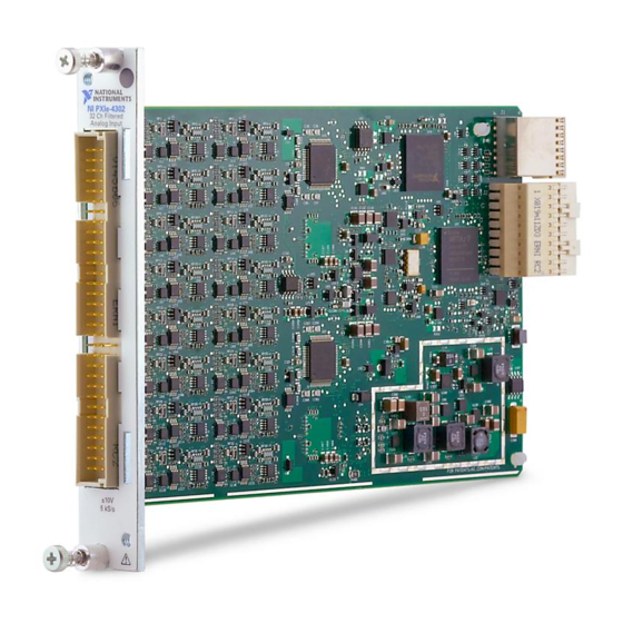
- Page 1 SC Express NI PXIe-4302/4303 User Manual 32 Ch, 24-bit, 5 kS/s or 51.2 kS/s Simultaneous Filtered Data Acquisition Module NI PXIe-4302/4303 User Manual August 2015 377003A-01...
- Page 2 Tel: 866 ASK MYNI (275 6964) NI Services For further support information, refer to the appendix. To comment on National Instruments documentation, refer to the National Instruments website at ni.com/info enter the Info Code feedback © 2015 National Instruments. All rights reserved.
- Page 3 National Instruments Corporation. National Instruments respects the intellectual property of others, and we ask our users to do the same. NI software is protected by copyright and other intellectual property laws. Where NI software may be used to reproduce software or other materials belonging to others, you may use NI software only to reproduce materials that you may reproduce in accordance with the terms of any applicable license or other legal restriction.
- Page 4 ™ The ExpressCard word mark and logos are owned by PCMCIA and any use of such marks by National Instruments is under license. The mark LabWindows is used under a license from Microsoft Corporation. Windows is a registered trademark of Microsoft Corporation in the United States and other countries.
-
Page 5: Table Of Contents
Connecting Thermocouple Signals................2-4 Cold-Junction Compensation ................2-4 Connecting Current Signals..................2-5 Module Pinout ......................2-6 I/O Connector Signal Descriptions................2-8 NI PXIe-4302/4303 Block Diagram................. 2-8 Signal Acquisition Considerations ................... 2-9 Nyquist Frequency and Nyquist Bandwidth............. 2-9 ADC.......................... 2-9 Operation Modes ...................... 2-9 Buffered Mode Acquisitions .................. - Page 6 Connecting a Loop-Powered Current Transducer ......... 2-6 Figure 2-8. Connecting a Three-Wire Current Transducer ........2-7 Figure 2-9. NI PXIe-4302/4303 Block Diagram............. 2-10 Figure 2-10. HWTSP Data Path Model..............2-14 Figure 2-11. Transfer Time and Application Time Relationship ....... 2-15 Figure 2-12.
-
Page 7: Getting Started
The NI PXIe-4302/4303 provides 32 simultaneously sampled filtered analog input channels. The NI PXIe-4302 can operate at sample rates up to 5 kS/s/ch and the NI PXIe-4303 can operate at sample rates up to 51.2 kS/s/ch. These modules can measure an analog voltage up to 10 V when using the TB-4302 and can measure 20 mA current signals when using the TB-4302C. -
Page 8: Using The Module
NI PXIe-4302/4303. It also provides the I/O connector signal pin assignments of the modules. Driver support for the NI PXIe-4302/4303 was first available in NI-DAQmx 15.1. For the list of devices supported by a specific release, refer to the NI-DAQmx Readme, available on the version-specific download page or installation media. -
Page 9: Figure 2-1. Connecting Floating Signal Source Without Bias Resistors
Chapter 2 Using the Module Figure 2-1. Connecting Floating Signal Source without Bias Resistors TB-4302 PXIe-4302/4303 Floating Signal – Source AI– AI– Impedance (<100 Ω) AIGND AIGND For source impedances ≥100 Ω, this connection leaves the differential signal path significantly off balance. -
Page 10: Figure 2-3. Connecting Floating Signal Source With Balanced Bias Resistors
NI PXIe-4302/4303 User Manual Figure 2-3. Connecting Floating Signal Source with Balanced Bias Resistors TB-4302 PXIe-4302/4303 Floating Signal – Source AI– AI– AIGND AIGND Both AI+ and AI- require a DC path to ground. If the source is AC coupled, a resistor is required between the positive input and AIGND, as shown in Figure 2-4. -
Page 11: Connecting Ground-Referenced Voltage Signal Sources
Follow the connection instructions for grounded signal sources to eliminate this ground potential difference from the measured signal. Figure 2-6 shows how to connect a ground-referenced signal source to an NI PXIe-4302/4303 with a TB-4302. Figure 2-6. Connecting Ground-Referenced Signal Sources... -
Page 12: Connecting Current Signals
AI channel. You can only connect one external voltage supply to the TB-4302C. The TB-4302C internally shorts all of the negative AI inputs of NI PXIe-4302/4303 to all of the AISENSE terminals on the TB-4302C terminal block. There are a total of 18 AISENSE terminals on the TB-4302C. -
Page 13: Module Pinout
AIGND AIGND Module Pinout Table 2-1 shows the pinout of the front connector of the NI PXIe-4302/4303. Refer to the Connector Signal Descriptions section for definitions of each signal. Refer to the NI PXIe-4302/4303 and TB-4302/4302C User Guide and Terminal Block Specifications for signal locations on the terminal blocks. -
Page 14: Table 2-1. Front Connector Signal Pin Assignments
NI PXIe-4302/4303 User Manual Table 2-1. Front Connector Signal Pin Assignments Front Connector Diagram Number Column A Column B Column C AIGND AI0+ AI1+ AI2+ AI0- AI1- Column AI2- AI3- AI3+ AIGND AI4+ AI5+ AI6+ AI4- AI5- AI6- AI7- AI7+... -
Page 15: I/O Connector Signal Descriptions
DGND. NI PXIe-4302/4303 Block Diagram Figure 2-9 shows the block diagram of the NI PXIe-4302/4303. The analog signal conditioning for each channel consists of a software selectable gain block and an anti-alias filter. Each conditioned signal is then digitized by a 24-bit delta-sigma ADC to achieve simultaneous data acquisition. -
Page 16: Signal Acquisition Considerations
The NI PXIe-4302 supports rates of 1 S/s to 5 kS/s. The NI PXIe-4303 supports rates of 1 S/s to 51.2 kS/s. -
Page 17: Buffered Mode Acquisitions
Buffered Mode Acquisitions In buffered mode, the NI PXIe-4302/4303 uses a combination of analog and digital filtering to provide an accurate representation of in-band signals while rejecting out-of-band signals. These filters discriminate between signals based on the frequency range, or bandwidth, of the signal. - Page 18 NI PXIe-4302/4303 and when the data associated with that event is available at the output of the acquisition and filtering process. This delay is called the group delay.
-
Page 19: Optional Buffered Mode Iir Filtering
For 51.2 kS/s, the digital filter group delay 48.5 S 1.79742 ms 1.79837 ms ---------------------- 51.2 kS/s If a 10 V range is used, total delay is 1.79837 ms + 6.77 μs = 1.80514 ms. Refer to the NI PXIe-4302/4303 Specifications for more information. 2-12 | ni.com... -
Page 20: Hardware-Timed Single Point Acquisitions
Hardware-Timed Single Point (HWTSP) is a hardware-timed acquisition mode in which a digital hardware signal (SampleClock) controls the rate of the acquisition. The SampleClock signal can be imported or internally generated on the NI PXIe-4302/4303 using the sample rate configured with a NI-DAQmx task. -
Page 21: Khz Control Loop Rate Calculation Example
Chapter 2 Using the Module Figure 2-11. Transfer Time and Application Time Relationship Acquisition Rate Period Transfer Application Time Wait Time (Idle) 20 μs * Next Sample Filter Group Delay 120 μs ** Sample Sample Clock Clock *Transfer time may vary depending on system. **120 μs is the approximate group delay of the 2 kHz filter for input frequencies <... -
Page 22: Timing And Triggering
Any application taking more than 480 μs will fail to close the 2 kHz control loop. When analyzing the bandwidth of the system, you must consider the group delay of all the components of the system. When using only the NI PXIe-4302/4303 internal 2 kHz filter, the bandwidth of the control loop is as follows:... -
Page 23: External Clock
Reference-triggered acquisitions can therefore only be configured as finite tasks. The analog trigger on the NI PXIe-4302/4303 cannot be used as a start trigger. This restriction is a result of the way the module compensates for the filter group delay. -
Page 24: Triggering And Filter Delay
PXIe chassis. Choose an arbitrary NI PXIe-4302/4303 master module to issue a sync pulse on one of the PXIe Trigger lines. The sync pulse resets the ADCs and oversample clocks, phase aligning all the clocks in the system to within nanoseconds. - Page 25 Consider the following caveat to using Reference Clock synchronization: • The NI PXIe-4302/4303 automatically compensates for its filter group delay. However, some other device families do not compensate for their filter delay. In this case, manually compensate for group delay in the waveforms when you synchronize between device families if this level of synchronization is required for your application.
-
Page 26: Timing Engines And Dsp Streams
When you create a task in software, that software task interacts with one or more timing engines in the NI PXIe-4302/4303. There are a total of four timing engines in hardware that can be operated simultaneously. Each of these timing engines can have individualized configuration settings for timing, triggering, and the sample mode. -
Page 27: Accessory Auto-Detection
Chapter 2 Using the Module • A task is set up and started using ai0 in buffered mode. A second task is created with ai0 also in buffered mode. The second task will produce an error since the first task is already using ai0. -
Page 28: Sc Express Considerations
Triggers can be used to synchronize the operation of several different PXI peripheral modules. © National Instruments | 3-1... -
Page 29: Pxi_Star Trigger
Chapter 3 SC Express Considerations In a PXI chassis with more than eight slots, the PXI trigger lines may be divided into multiple independent buses. Refer to the documentation for your chassis for details. PXI_STAR Trigger In a PXI Express system, the Star Trigger bus implements a dedicated trigger line between the system timing slot and the other peripheral slots. -
Page 30: Ni Services
NI Services National Instruments provides global services and support as part of our commitment to your success. Take advantage of product services in addition to training and certification programs that meet your needs during each phase of the application life cycle; from planning and development through deployment and ongoing maintenance. - Page 31 Appendix A NI Services – The Skills Guide assists you in identifying the proficiency requirements of your current application and gives you options for obtaining those skills consistent with your time and budget constraints and personal learning preferences. Visit ni.com/ to see these custom paths.
Need help?
Do you have a question about the PXIe-4302 and is the answer not in the manual?
Questions and answers