
Related Manuals for NXP Semiconductors QorIQ LS1043ARDB


Summary of Contents for NXP Semiconductors QorIQ LS1043ARDB
- Page 1 QorIQ LS1043A Reference Design Board Reference Manual Document Number: LS1043ARDBRM Rev. 4, 11/2017...
- Page 2 QorIQ LS1043A Reference Design Board Reference Manual, Rev. 4, 11/2017 NXP Semiconductors...
-
Page 3: Table Of Contents
2.5.1 Mini-PCIe card..............................27 2.6 USB interface..................................28 2.7 I2C interface..................................29 Chapter 3 Power Supplies and CPLD Controller 3.1 Power supply block diagram.............................33 3.2 Power supply operation..............................34 3.2.1 Power ON................................34 QorIQ LS1043A Reference Design Board Reference Manual, Rev. 4, 11/2017 NXP Semiconductors... - Page 4 PCBA version register (CPLD_PCBA_VER)..................... 53 6.1.4 System reset register (CPLD_SYSTEM_RST)....................53 6.1.5 CPLD override physical switches enable register (CPLD_SOFT_MUX_ON)...........54 6.1.6 POR RCW source location register 1 (CPLD_REG_RCW_SRC1)..............55 QorIQ LS1043A Reference Design Board Reference Manual, Rev. 4, 11/2017 NXP Semiconductors...
- Page 5 6.1.16 RTC clock assignment register (CPLD_REG_RTC)...................61 6.1.17 EVDD control register (CPLD_EVDD_SEL)..................... 62 6.1.18 CPLD register override physical switch SDHC_VS/SPI_CS0 enable register (CPLD_SOFT_VS_SPICS0)..62 6.1.19 SDHC_VS or SPI_CS0 selection register (CPLD_VS_SPICS0_SEL)............... 63 QorIQ LS1043A Reference Design Board Reference Manual, Rev. 4, 11/2017 NXP Semiconductors...
- Page 6 QorIQ LS1043A Reference Design Board Reference Manual, Rev. 4, 11/2017 NXP Semiconductors...
- Page 7 A software application developed for the LS1043ARDB can run with various input/ output data streams, for example, PCIe or XFI connections. The board support package (BSP) is developed using the Linux operating system. QorIQ LS1043A Reference Design Board Reference Manual, Rev. 4, 11/2017 NXP Semiconductors...
-
Page 8: Acronyms And Abbreviations
Inter-integrated circuit multi-master serial computer bus Integrated flash controller Initial program load JTAG Joint Test Action Group (IEEE® standard 1149.1™) LBMAP Local bus map Table continues on the next page... QorIQ LS1043A Reference Design Board Reference Manual, Rev. 4, 11/2017 NXP Semiconductors... - Page 9 Secure interfaces and power SLAC Subscriber line access controller Single-level cell SLIC Subscriber line interface controller Subminiature version B connector Serial presence detect Table continues on the next page... QorIQ LS1043A Reference Design Board Reference Manual, Rev. 4, 11/2017 NXP Semiconductors...
-
Page 10: Related Documentation
This table lists and describes the additional documents available for more information on the LS1043ARDB. Table 1-2. Related documentation Document Description QorIQ LS1043ARDB Getting Started Guide Describes the LS1043ARDB hardware kit, provides settings for the (LS1043ARDBGSG) onboard switches, connectors, jumpers, and LEDs, and explains the basic board operations in a step-by-step manner... -
Page 11: Board Features
• Provides clocks to all SerDes blocks and slots • 100 MHz or 156.25 MHz for PLL1 • 100 MHz for PLL2 • Supports 32.768 kHz for RTC Table continues on the next page... QorIQ LS1043A Reference Design Board Reference Manual, Rev. 4, 11/2017 NXP Semiconductors... -
Page 12: Block Diagrams
TA_BB_VDD, the LS1043A processor supports 1.0 V as well as 0.9 V; however, the LS1043ARDB only supports 1.0 V. 1.4 Block diagrams The figure below shows the LS1043A processor block diagram. QorIQ LS1043A Reference Design Board Reference Manual, Rev. 4, 11/2017 NXP Semiconductors... - Page 13 4-Lane, 10 GHz SerDes Core Complex Accelerators and Memory Control Basic Peripherals, Interconnect and Debug Networking Elements Figure 1-1. LS1043A processor block diagram The figure below shows the LS1043ARDB block diagram. QorIQ LS1043A Reference Design Board Reference Manual, Rev. 4, 11/2017 NXP Semiconductors...
-
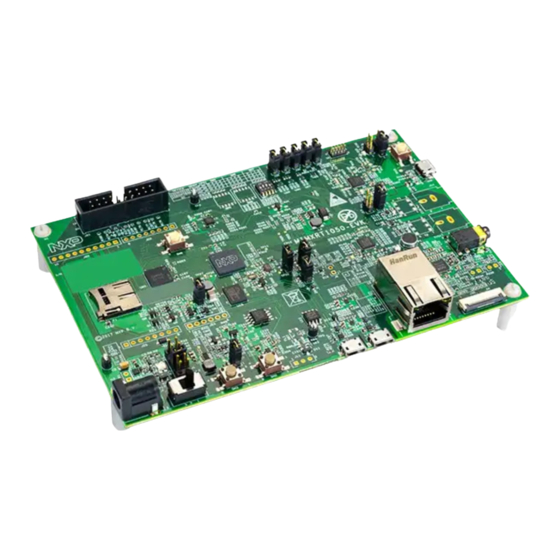
Page 14: Board Views
16 MB EEPROM JTAG header Board components Clocks +12 V Connectors Expansion modules Figure 1-2. LS1043ARDB block diagram 1.5 Board views The figure below shows the LS1043ARDB top view. QorIQ LS1043A Reference Design Board Reference Manual, Rev. 4, 11/2017 NXP Semiconductors... - Page 15 TDM slot Mini-PCIe slot Chassis fan RTC battery CPU JTAG K22 JTAG Mini-USB to UART1 Figure 1-3. LS1043ARDB top view The figure below shows the LS1043ARDB bottom view. QorIQ LS1043A Reference Design Board Reference Manual, Rev. 4, 11/2017 NXP Semiconductors...
- Page 16 Board views Figure 1-4. LS1043ARDB bottom view QorIQ LS1043A Reference Design Board Reference Manual, Rev. 4, 11/2017 NXP Semiconductors...
-
Page 17: Interfaces
SDRAM discrete devices (32-bit bus). The memory interface includes all necessary termination and I/O powers. It is routed such that maximum performance of the memory bus can be achieved. The figure below shows the DDR memory architecture. QorIQ LS1043A Reference Design Board Reference Manual, Rev. 4, 11/2017 NXP Semiconductors... -
Page 18: Ifc Interface
• Supports the following IFC clients on the LS1043ARDB: • NAND flash (async/sync - ONFI 1.0 compatible) • NOR flash 16-bit The figure below shows the IFC block diagram. QorIQ LS1043A Reference Design Board Reference Manual, Rev. 4, 11/2017 NXP Semiconductors... -
Page 19: Nor Flash Memory
Data width 000100101 NOR flash 16 bits NAND flash 8 bits CPLD registers 8 bits 100000110 NAND flash 8 bits NOR flash 16 bits CPLD registers 8 bits QorIQ LS1043A Reference Design Board Reference Manual, Rev. 4, 11/2017 NXP Semiconductors... -
Page 20: Nand Flash Memory
The LS1043ARDB has several serial interfaces, such as RS-232, DSPI, eSDHC/eMMC, and I2C. This section describes the following main serial interfaces used in the LS1043ARDB: • UART interface • eSDHC interface • DSPI interface QorIQ LS1043A Reference Design Board Reference Manual, Rev. 4, 11/2017 NXP Semiconductors... -
Page 21: Uart Interface
UART2 (J4 top) 2.3.2 eSDHC interface The LS1043ARDB enhanced secure digital high capacity card (eSDHC) has the following features: • x1/x4-bit SD card supporting SD Rev 2.0 and 3.0. QorIQ LS1043A Reference Design Board Reference Manual, Rev. 4, 11/2017 NXP Semiconductors... - Page 22 Supply voltage negative Pin 5 Supply voltage positive Pin 6 Clock signal Pin 7 Supply voltage negative Pin 8 DAT0 Data signal 0 Pin 9 DAT1 Data signal 1 QorIQ LS1043A Reference Design Board Reference Manual, Rev. 4, 11/2017 NXP Semiconductors...
-
Page 23: Dspi Interface
OVDD Level SPI_CS1 = 1.8 V header shifter 3.3 V SPI_CS1_B SPI_CS2 Level SPI_CS3 shifter 1.8 V 3.3 V 3.3 V SPI_CS[2:3]_B riser card Figure 2-5. DSPI connections QorIQ LS1043A Reference Design Board Reference Manual, Rev. 4, 11/2017 NXP Semiconductors... -
Page 24: Ethernet Interface
EC port connected to a Realtek RTL8211FS PHY on the LS1043ARDB. LS1043A RTL8211FS eTSEC2 Address 2 RTL8211FS eTSEC1 Address 1 MDIO/MDC EMI1_MDC/MDIO Figure 2-6. Ethernet interface QorIQ LS1043A Reference Design Board Reference Manual, Rev. 4, 11/2017 NXP Semiconductors... -
Page 25: Ethernet Management Interfaces
Table 2-6. PHYs connected with EMIs Manufacturer part number Manufacturer name PHY type RTL8211FS Realteck RGMII F104S8A NXP Semiconductors QSGMII AQR105-B1 Aquantia The figure below shows how PHY transceivers are connected with EMIs. QorIQ LS1043A Reference Design Board Reference Manual, Rev. 4, 11/2017 NXP Semiconductors... -
Page 26: Serdes Interface
Part number Manufacturer Description AQR105-B1 Aquantia Ethernet single-port AQrate 10GBase-T PHY FCBGA324 F104S8A NXP Semiconductors VSC8514, quad-port 10/100/1000Base-T PHY with QSGMII MAC Table continues on the next page... QorIQ LS1043A Reference Design Board Reference Manual, Rev. 4, 11/2017 NXP Semiconductors... -
Page 27: Mini-Pcie Card
(10G) eth1 eth5 QSGMII Rx/Tx 1 (4x1.25G) eth0 Mini-PCIe slot eth4 Rx/Tx 2 (PCIe 2) PCIe slot x1 Rx/Tx 3 (PCIe 3) Figure 2-8. LS1043ARDB SerDes lane connections QorIQ LS1043A Reference Design Board Reference Manual, Rev. 4, 11/2017 NXP Semiconductors... -
Page 28: Usb Interface
5 V power. The power enable and power-fault-detect pins are connected to the LS1043A processor via CPLD for individual port management. The figure below shows the LS1043ARDB USB architecture. QorIQ LS1043A Reference Design Board Reference Manual, Rev. 4, 11/2017 NXP Semiconductors... -
Page 29: I2C Interface
• LS1043A I2C2, I2C3, and I2C4 are not used as I2C but they are used as other multiplexed pin functions. The figure below shows the overall I2C scheme connections. QorIQ LS1043A Reference Design Board Reference Manual, Rev. 4, 11/2017 NXP Semiconductors... - Page 30 EEPROM for DDR. The other half is used as a store system ID and MAC address. 0x4C SA56004ED NXP Semiconductors Thermal monitor 0x08 PC34VR500V4 NXP Semiconductors Power management integrated circuit (PMIC) for the onboard powers 0x69 6V49205BNLGI Clock generator 0x40 INA220AIDGST Texas Instruments...
- Page 31 7-bit addresses do not include the R/W bit as an address member, though some datasheets might do so. For consistency, all I2C addresses are of 7 bits only. QorIQ LS1043A Reference Design Board Reference Manual, Rev. 4, 11/2017 NXP Semiconductors...
- Page 32 I2C interface QorIQ LS1043A Reference Design Board Reference Manual, Rev. 4, 11/2017 NXP Semiconductors...
-
Page 33: Power Supplies And Cpld Controller
3.1 Power supply block diagram The figure below shows the LS1043ARDB power supply block diagram. QorIQ LS1043A Reference Design Board Reference Manual, Rev. 4, 11/2017 NXP Semiconductors... -
Page 34: Power Supply Operation
The power supply operation involves the following two activities: • Power ON • Power sequencing 3.2.1 Power ON The SW2 switch, which is on the rear panel enables the 12 V power supply for the board. QorIQ LS1043A Reference Design Board Reference Manual, Rev. 4, 11/2017 NXP Semiconductors... -
Page 35: Cpld Controller
• Control status LED • Map/re-map the LS1043A local bus chip selects and ready and busy signals to NOR flash and NAND flash • IFC bus control: QorIQ LS1043A Reference Design Board Reference Manual, Rev. 4, 11/2017 NXP Semiconductors... -
Page 36: Cpld Block Diagram
• NOR bank selection: Split NOR flash into 8 banks. 3.3.2 CPLD block diagram The figure below shows a detailed block diagram of the CPLD controller on the LS1043ARDB. QorIQ LS1043A Reference Design Board Reference Manual, Rev. 4, 11/2017 NXP Semiconductors... -
Page 37: Cpld Registers
LS1043ARDB. These registers can be accessed from CPLD using IFC. The table below shows the peripheral data bus width and memory map for CPLD. QorIQ LS1043A Reference Design Board Reference Manual, Rev. 4, 11/2017 NXP Semiconductors... -
Page 38: Power-On Reset
HRESET_B indicates the hard reset input signal. It is a bi-directional open drain signal. It functions as an output signal during initial steps in the POR sequence. The table below describes the POR sequence. QorIQ LS1043A Reference Design Board Reference Manual, Rev. 4, 11/2017 NXP Semiconductors... -
Page 39: Reset Configuration Signals
Specifies RCW fetch location CFG_RCW_SRC4 IFC_AD11 SW4[5] Specifies RCW fetch location CFG_RCW_SRC5 IFC_AD12 SW4[6] Specifies RCW fetch location CFG_RCW_SRC6 IFC_AD13 SW4[7] Specifies RCW fetch location Table continues on the next page... QorIQ LS1043A Reference Design Board Reference Manual, Rev. 4, 11/2017 NXP Semiconductors... -
Page 40: Reset Architecture
The reset signals sent to and received from the LS1043A processor and other devices on the LS1043ARDB are managed by the CPLD controller. The figure below shows the LS1043ARDB reset architecture. QorIQ LS1043A Reference Design Board Reference Manual, Rev. 4, 11/2017 NXP Semiconductors... -
Page 41: Ddr Supply
0.6 V <= 1 A Bus termination supply +2V5_VPP 2.5 V < 200 mA DRAM activating power supply The LS1043ARDB uses the VR500 (U33) switching power controller as follows: QorIQ LS1043A Reference Design Board Reference Manual, Rev. 4, 11/2017 NXP Semiconductors... -
Page 42: Povdd Supply
3.6 POVDD supply J12 and J13 connectors on the LS1043ARDB connect POVDD power line to LS1043A PROG_MTR and PROG_SFP pins. Otherwise, they are pulled down to the ground plane. QorIQ LS1043A Reference Design Board Reference Manual, Rev. 4, 11/2017 NXP Semiconductors... -
Page 43: Clocks, Interrupts, And Temperature Monitoring
Temperature anode and cathode 4.1 Clocking scheme The figure below shows the LS1043ARDB clocking scheme. NOTE For RDBs, NXP Semiconductors does not support spread spectrum for SerDes clocking. QorIQ LS1043A Reference Design Board Reference Manual, Rev. 4, 11/2017 NXP Semiconductors... -
Page 44: Clock Frequency Selection
The table below shows how to select SYSCLK frequency based on the settings of the SW3 switch. Table 4-1. SYSCLK frequency selection SW3[1] SW3[2] Selected SYSCLK frequency 66.67 MHz 100.00 MHz (default value) 80.00 MHz Table continues on the next page... QorIQ LS1043A Reference Design Board Reference Manual, Rev. 4, 11/2017 NXP Semiconductors... -
Page 45: Mpic Controller
SA56004ED temperature warning and alarm signals are used to drive indicators and are connected to CPLD for monitoring. CPLD uses these signals to power down the system to protect the LS1043ARDB from over-temperature failure. QorIQ LS1043A Reference Design Board Reference Manual, Rev. 4, 11/2017 NXP Semiconductors... - Page 46 Temperature anode and cathode QorIQ LS1043A Reference Design Board Reference Manual, Rev. 4, 11/2017 NXP Semiconductors...
-
Page 47: Debug And Input/Output
Debug and Input/Output This chapter contains the following sections: • ARM/JTAG architecture • CMSIS-DAP • GPIOs 5.1 ARM/JTAG architecture The ARM/JTAG architecture is shown in the figure below. QorIQ LS1043A Reference Design Board Reference Manual, Rev. 4, 11/2017 NXP Semiconductors... -
Page 48: Cmsis-Dap
This section describes the MBED circuit on the LS1043ARDB. MBED is an open standard serial and debug adapter. It bridges serial and debug communications between a USB host and an embedded target processor, as shown in the figure below. QorIQ LS1043A Reference Design Board Reference Manual, Rev. 4, 11/2017 NXP Semiconductors... -
Page 49: Gpios
Some GPIO pins are connected to a test point to allow access. The names of the GPIO pins with and without test point access are shown in the table below. QorIQ LS1043A Reference Design Board Reference Manual, Rev. 4, 11/2017 NXP Semiconductors... - Page 50 TDM slot IRQ[8] GPIO1_28 TDMB_RXD TDM slot IRQ[9] GPIO1_29 TDMB_RSYNC TDM slot IRQ[10] GPIO1_30 TDMB_TXD TDM slot IRQ[11] GPIO1_31 CPLD ASLEEP GPIO1_13 ALEEP LED GPIO1_14 RTC CLK RTC clock QorIQ LS1043A Reference Design Board Reference Manual, Rev. 4, 11/2017 NXP Semiconductors...
-
Page 51: Cpld Programming
(CPLD_SD1REFCLK_SEL) TDM clock or SDHC/USB selection register See section 6.1.12/59 (CPLD_TDMCLK_MUX_SEL) Status LED control register (CPLD_STATUS_LED) 6.1.13/60 Global reset register (CPLD_GLOBAL_RST) 6.1.14/60 Table continues on the next page... QorIQ LS1043A Reference Design Board Reference Manual, Rev. 4, 11/2017 NXP Semiconductors... -
Page 52: Cpld Major Version Register (Cpld_Ver)
This field is reserved. 6.1.2 CPLD minor version register (CPLD_VER_SUB) Use this register to specify CPLD minor version. Address: 0h base + 1h offset = 1h Read VER_SUB Reserved Write Reset QorIQ LS1043A Reference Design Board Reference Manual, Rev. 4, 11/2017 NXP Semiconductors... -
Page 53: Pcba Version Register (Cpld_Pcba_Ver)
Address: 0h base + 3h offset = 3h Read SYSTEM_ Reserved Write Reset CPLD_SYSTEM_RST field descriptions Field Description System reset SYSTEM_RST Table continues on the next page... QorIQ LS1043A Reference Design Board Reference Manual, Rev. 4, 11/2017 NXP Semiconductors... -
Page 54: Cpld Override Physical Switches Enable Register (Cpld_Soft_Mux_On)
SerDes PLL1 reference clock input control enable SD1REFCLK_ SerDes PLL1 reference clock input control disable (default value) IN_CTRL_EN SerDes PLL1 reference clock input control enable Table continues on the next page... QorIQ LS1043A Reference Design Board Reference Manual, Rev. 4, 11/2017 NXP Semiconductors... -
Page 55: Por Rcw Source Location Register 1 (Cpld_Reg_Rcw_Src1)
CFG_RCW_SRC[0:7] Write Reset * Notes: • The register reset value is controlled by SW4[1] - SW4[8]. CPLD_REG_RCW_SRC1 field descriptions Field Description 0–7 POR RCW source location CFG_RCW_ SRC[0:7] QorIQ LS1043A Reference Design Board Reference Manual, Rev. 4, 11/2017 NXP Semiconductors... -
Page 56: Por Rcw Source Location Register 2 (Cpld_Reg_Rcw_Src2)
* Notes: • The register reset value is controlled by SW5[4] - SW5[6]. CPLD_REG_BANK field descriptions Field Description 0–2 Bank control bits BANK_CTRL Table continues on the next page... QorIQ LS1043A Reference Design Board Reference Manual, Rev. 4, 11/2017 NXP Semiconductors... -
Page 57: System Clock Single-Ended Or Differential Input Selection Register (Cpld_Sysclk_Sel)
The register reset value is controlled by SW5[2]. CPLD_SYSCLK_SEL field descriptions Field Description System clock input selection SYSCLK_IN_ System clock differential input (default value) System clock single-ended input 1–7 This field is reserved. QorIQ LS1043A Reference Design Board Reference Manual, Rev. 4, 11/2017 NXP Semiconductors... -
Page 58: Uart1 Output Selection Register (Cpld_Uart_Sel)
Address: 0h base + Ah offset = Ah Read SD1REFCLK_SEL Reserved Write Reset Read Reserved Write Reset * Notes: • The register reset value is controlled by SW3[4]. QorIQ LS1043A Reference Design Board Reference Manual, Rev. 4, 11/2017 NXP Semiconductors... -
Page 59: Tdm Clock Or Sdhc/Usb Selection Register (Cpld_Tdmclk_Mux_Sel)
The register reset value is controlled by SW3[7]. CPLD_TDMCLK_MUX_SEL field descriptions Field Description TDM clock or SDHC/USB selection TDMCLK_ TDM_CLK SDHC_USB_SEL SDHC/USB (default value) 1–7 This field is reserved. QorIQ LS1043A Reference Design Board Reference Manual, Rev. 4, 11/2017 NXP Semiconductors... -
Page 60: Status Led Control Register (Cpld_Status_Led)
Address: 0h base + Eh offset = Eh Read GLOBAL_ Reserved Write Reset CPLD_GLOBAL_RST field descriptions Field Description System is running (default value) GLOBAL_RST System is reset 1–7 This field is reserved. QorIQ LS1043A Reference Design Board Reference Manual, Rev. 4, 11/2017 NXP Semiconductors... -
Page 61: Tdm Riser Card Presence Detection Register (Cpld_Tdmr_Prs_N)
CPLD_REG_RTC field descriptions Field Description RTC clock assignment to RTC (only assert from LS1043ARDB Rev. B board) RTC_CLK_ Reserved (default value) ASSGNMT To RTC Table continues on the next page... QorIQ LS1043A Reference Design Board Reference Manual, Rev. 4, 11/2017 NXP Semiconductors... -
Page 62: Evdd Control Register (Cpld_Evdd_Sel)
Use this register to enable CPLD register value override physical switch to select SDHC_VS or SPI_CS0. Address: 0h base + 12h offset = 12h Read VS_SPICS0_EN Reserved Write Reset Read Reserved Write Reset QorIQ LS1043A Reference Design Board Reference Manual, Rev. 4, 11/2017 NXP Semiconductors... -
Page 63: Sdhc_Vs Or Spi_Cs0 Selection Register (Cpld_Vs_Spics0_Sel)
The register reset value is controlled by SW3[8]. CPLD_VS_SPICS0_SEL field descriptions Field Description SDHC_VS or SPI_CS0 CPLD selection VS_SPICS0_SEL SDHC_VS (default value) SPI_CS0 1–7 This field is reserved. QorIQ LS1043A Reference Design Board Reference Manual, Rev. 4, 11/2017 NXP Semiconductors... - Page 64 CPLD memory map / register definitions QorIQ LS1043A Reference Design Board Reference Manual, Rev. 4, 11/2017 NXP Semiconductors...
- Page 65 V1.1, 1.6 GHz SCH-28529 Rev. D , LAY-28529 Rev. D, E (buffer, USB switch, level D1, E shifter, temperature sensor, and so on) from other vendors with components from NXP QorIQ LS1043A Reference Design Board Reference Manual, Rev. 4, 11/2017 NXP Semiconductors...
- Page 66 QorIQ LS1043A Reference Design Board Reference Manual, Rev. 4, 11/2017 NXP Semiconductors...
- Page 67 Removed TA_BB_RTC instances from the document as TA_BB_RTC has been defeatured Removed CFG_SVR instances from the document Rev. 2 08/2016 eSDHC interface Updated the section Table continues on the next page... QorIQ LS1043A Reference Design Board Reference Manual, Rev. 4, 11/2017 NXP Semiconductors...
- Page 68 • Changed the reset value of the definitions CPLD_VER_SUB register to 04h • Changed the reset value of the CPLD_PCBA_VER register to 03h Rev. 0 08/2015 Initial public release QorIQ LS1043A Reference Design Board Reference Manual, Rev. 4, 11/2017 NXP Semiconductors...
- Page 69 How to Reach Us: Information in this document is provided solely to enable system and software implementers to use NXP products. There are no express or implied copyright Home Page: licenses granted hereunder to design or fabricate any integrated circuits based nxp.com on the information in this document.
Need help?
Do you have a question about the QorIQ LS1043ARDB and is the answer not in the manual?
Questions and answers