Table of Contents
Advertisement
Advertisement
Table of Contents

Related Manuals for Nordic nRF5340


Summary of Contents for Nordic nRF5340
- Page 1 PDK User Guide v1.0 4406_489 v1.0 / 2019-11-13...
-
Page 2: Table Of Contents
......5.3.4 nRF5340 power source ...... - Page 3 Glossary ........Acronyms and abbreviations .
-
Page 4: Revision History
Revision history Date Version Description November 2019 1.0 First release 4406_489 v1.0... -
Page 5: Introduction
Introduction The nRF5340 Preview Development Kit (PDK) includes hardware, firmware source code, documentation, hardware schematics, and layout files. The key features of the development kit are: • Support for nRF5340 System on Chip (SoC) development • Support for the following wireless protocols: ®... -
Page 6: Minimum Requirements
Minimum requirements Before you start, check that you have the required hardware and software. Hardware requirements • Personal computer (PC) or Mac • Micro-USB 2.0 cable Software requirements • Operating system: Windows 7, Windows 8, Windows 10, MacOS, or Linux •... -
Page 7: Kit Content
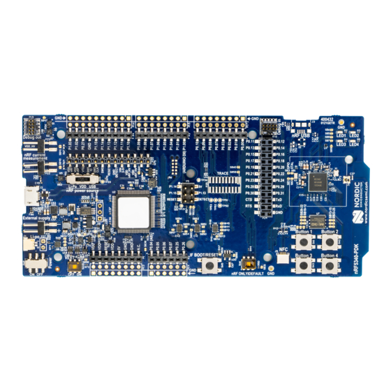
Figure 1: nRF5340 PDK board (PCA10095) and NFC antenna 3.2 Downloadable content The nRF5340 PDK downloadable content includes the hardware files. Hardware files Schematics, layout, bill of materials, and Gerber files for the nRF5340 PDK are included in a zip file. • nRF5340 PDK Downloads 3.3 Related documentation In addition to the information in this document, you may need to consult other documents. - Page 8 Kit content • nRF Connect SDK 4406_489 v1.0...
-
Page 9: Interface Mcu
Interface MCU The interface MCU on the nRF5340 PDK board runs SEGGER J-Link OB interface firmware and is used to program and debug the firmware of the nRF5340 SoC. Figure 2: Interface MCU 4.1 IF Boot/Reset button The nRF5340 PDK board is equipped with an IF Boot/Reset button (SW5). -
Page 10: Dynamic Hwfc Handling
P0.21 P0.22 Table 1: Relationship of UART connections on nRF5340 and interface MCU The UART signals are routed directly to the interface MCU. The UART pins connected to the interface MCU are tri-stated when no terminal is connected to the virtual COM port on the computer. - Page 11 Interface MCU You can also disable the MSD of the kit by using the msddisable command in J-Link Commander. To enable, use the msdenable command. These commands take effect after a power cycle of the development kit and stay this way until changed again. 4406_489 v1.0...
-
Page 12: Hardware Description
Hardware description The nRF5340 PDK board PCA10095 can be used as a development platform for the nRF5340 SoC. It features an onboard programming and debugging solution. In addition to radio communication, the nRF5340 SoC can communicate with a computer through USB and a virtual COM port provided by the interface MCU. -
Page 13: Power Supply
Power switch Figure 5: Block diagram 5.3 Power supply The nRF5340 PDK board PCA10095 has multiple power options. The power options are: • USB connector J2 for the interface MCU (5 V) • Lithium polymer (Li-Po) battery connectors J6 or P27 (2.5–5.0 V) •... -
Page 14: Power Sources
The power sources are routed through a set of load switches, which is controlled by logic to give the correct priority of the power sources. If the high voltage regulator of the nRF5340 is used, the board will be supplied from the VDD_nRF voltage follower regardless of the state of the other power sources. - Page 15 Hardware description Figure 9: Power supply circuitry 4406_489 v1.0...
-
Page 16: Interface Mcu Power
Hardware description The power switches work in the way that the body diode of the internal transistor powers the VSUPPLY net, which supplies the gates controlling the enable signal of the switches. If 5 V is present, the switches for external supply and battery are disabled. If external supply is present, the switch for the battery is disabled. -
Page 17: Nrf5340 Power Source
19 for more information. 5.3.4 nRF5340 power source The nRF5340 PDK board has a power source switch (SW9) for selecting between three power sources for the nRF5340 SoC. The three positions of the switch are: • VDD (default) •... -
Page 18: Nrf5340 Direct Supply
Hardware description The nRF5340 SoC has a high voltage buck regulator that can support up to 5 V input. In the VDD position, the SoC is powered either from the on-board buck regulator, coin cell battery, or external supply (P21). -
Page 19: Operating Modes
Hardware description Since it is only the nRF5340 SoC that is supplied from this source, it is recommended to supply the VDD domain from a different source to prevent the pins of the SoC to be connected to unpowered devices. -
Page 20: Signal Switches
MCU can be disconnected either by unplugging the USB cable in J2 or by toggling SW6. The signal controls a set of switches (U3, U5, U6) that break the connection between the nRF5340 and the interface MCU, and control the power for the interface MCU. For more information, see section... -
Page 21: External Memory
Figure 18: Solder bridges: Shield detect and reset behavior 5.5 External memory The nRF5340 PDK board has a 64 Mb external flash memory. The memory is a multi-I/O memory supporting both regular SPI and Quad SPI. The memory is connected to the chip using the following GPIOs:... -
Page 22: Connector Interface
(SW6). In the nRF only mode, there are two optional power sources for keeping the external memory powered, VDD and VDD_nRF. If VDD_nRF is selected, the power consumption of the external memory will be added to the nRF5340 current measured on P22 or P23. See the following table for configuration:... - Page 23 Some of the signals are also available on connectors P7, P8, P9, P10, P11, and P12, which are on the bottom side of the board. By mounting pin lists on the connector footprints, the nRF5340 PDK board can be used as a shield for Arduino motherboards or other boards that follow the Arduino standard.
-
Page 24: Mapping Of Analog Pins
P0.06 AIN4 P0.07 AIN5 P0.25 AIN6 P0.26 AIN7 Table 5: Mapping of analog pins 5.7 Buttons and LEDs The four buttons and four LEDs on the nRF5340 PDK board are connected to dedicated GPIOs on the nRF5340 chip. 4406_489 v1.0... -
Page 25: Khz Crystal
The LEDs are active low, meaning that writing a logical zero ('0') to the output pin will illuminate the LED. Figure 23: Button and LED configuration 5.8 32.768 kHz crystal The nRF5340 SoC can use an optional 32.768 kHz crystal (X2) for higher accuracy and lower average power consumption. 4406_489 v1.0... -
Page 26: Debug Input And Trace
Hardware description On the nRF5340 PDK board, P0.00 and P0.01 are used for the 32.768 kHz crystal by default and are not available as GPIO on the connectors. ™ Note: When using ANT/ANT+ , the 32.768 kHz crystal (X2) is required for correct operation. -
Page 27: Debug Output
Note: The voltage supported by external debugging/programming is VDD voltage. Normally, this is 3 V when running from USB, but if the onboard nRF5340 SoC is supplied from either USB or Li- Ion, the nRF power source switch (SW9) is in either Li-Po or USB position, and VDD can be set by the nRF5340 firmware. -
Page 28: Nfc Antenna Interface
Debug out connector (P19). To enable this, short solder bridge SB47. Note that as long as SB47 is shorted, it is not possible to program the onboard nRF5340 SoC even if the external board is unplugged. -
Page 29: Extra Op-Amp
For more information on the power supply, see section Power supply on page 13. Figure 30: Extra op-amp 5.13 Solder bridge configuration This complete overview of solder bridges on the nRF5340 PDK helps to change the default state. Solderbridge Default Function Closed Cut to disconnect the 32.768 kHz on P0.01... - Page 30 Open Short to bypass the interface MCU USB power switch SB50 Closed Cut to disconnect the nRF5340 CTS line from the signal switch and interface MCU SB51 Closed Cut to disconnect the nRF5340 RTS line from the signal switch and...
- Page 31 Hardware description Solderbridge Default Function SB53 Closed Cut to disconnect the nRF5340 TxD line from the signal switch and interface MCU SB54 Closed Cut to disconnect the nRF5340 SWDIO line from the signal switch and interface MCU SB55 Closed Cut to disconnect the nRF5340 SWDCLK line from the signal switch...
-
Page 32: Measuring Current
Using an ampere-meter for current measurement on page 34. The nRF5340 SoC has two possible power supplies, VDD (1.7–3.6 V) and VDDH (2.5–5.5 V). The nRF5340 PDK is prepared for measuring current on both domains. Only the VDD domain current measurement is described here, but the approach is the same with the VDDH supply. -
Page 33: Using An Oscilloscope For Current Profile Measurement
• To restore normal kit function after measurement, solder SB40 or apply a jumper on P22. • To reprogram the nRF5340 SoC while the board is prepared for current measurements, remove measurement devices from P22, and then connect the USB cable. -
Page 34: Using An Ampere-Meter For Current Measurement
Use a minimum of 200 kSa/s (one sample every 5 µs) to get the correct average current measurement. 6.3 Using an ampere-meter for current measurement The average current drawn by the nRF5340 SoC can be measured using an ampere-meter. This method will monitor the current in series with the nRF device. - Page 35 Measuring current Note: An ampere-meter will measure the average current drawn by the nRF5340 SoC if: • The SoC is in a state where it draws a constant current, or, the activity on the device changing load current, like BLE connection events, is repeated continuously and has a short cycle time (less than 100 ms) so that the ampere-meter will average whole load cycles and not parts of the cycle.
-
Page 36: Rf Measurements
RF measurements The nRF5340 PDK board is equipped with a small coaxial connector (J1) for conducting measurements of the RF signal using a spectrum analyzer. The connector is of SWF type (Murata part no. MM8130-2600) with an internal switch. By default, when no cable is attached, the RF signal is routed to the onboard trace antenna. -
Page 37: Glossary
Glossary Clear to Send (CTS) In flow control, the receiving end is ready and telling the far end to start sending. Data Terminal Ready (DTR) A control signal in RS-232 serial communications transmitted from data terminal equipment, such as a computer, to data communications equipment. DK (Development Kit) A development platform used for application development. - Page 38 An RMS meter calculates the equivalent direct current (DC) value of an alternating current (AC) waveform. A true-RMS meter can accurately measure both pure waves and the more complex nonsinusoidal waves. SubMiniature Version A (SMA) Connector A semi-precision coaxial RF connector for coaxial cables with a screw-type coupling mechanism. System on Chip (SoC) A microchip that integrates all the necessary electronic circuits and components of a computer or other electronic systems on a single integrated circuit.
-
Page 39: Acronyms And Abbreviations
Acronyms and abbreviations These acronyms and abbreviations are used in this document. Clear to Send Data Terminal Ready HWFC Hardware Flow Control Integrated Development Environment Mass Storage Device Near Field Communication op-amp Operational Amplifier Preview Development Kit Root Mean Square Request to Send Receive Data SubMiniature version A... -
Page 40: Fcc Regulatory Notice
FCC regulatory notice The following regulatory notices apply to the nRF5340 PDK. This kit has not been authorized under the rules of the FCC and is designed to allow: • Product developers to evaluate electronic components, circuitry, or software associated with the kit to determine whether to incorporate such items in a finished product. -
Page 41: Legal Notices
Nordic Semiconductor ASA customers using or selling these products for use in such applications do so at their own risk and agree to fully indemnify Nordic Semiconductor ASA for any damages resulting from such improper use or sale.
Need help?
Do you have a question about the nRF5340 and is the answer not in the manual?
Questions and answers