Advertisement
Quick Links
Advertisement

Related Manuals for Fostex VM200


Summary of Contents for Fostex VM200
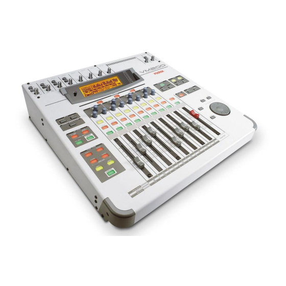
- Page 1 Service Manual Model VM200 DIGITAL RECORDING MIXER...
- Page 2 CAUTION: CAUTION TO PREVENT ELECTRIC SHOCK, MATCH RISK OF ELECTRIC SHOCK WIDE BLADE OF PLUG TO WIDE SLOT, DO NOT OPEN FULLY INSERT. ATTENTION: CAUTION: TO REDUCE THE RISK OF ELECTRIC SHOCK, POUR ÉVITER LES CHOCS ÉLECTRIQUES, DO NOT REMOVE COVER (OR BACK). INTRODUIRE LA LAME LA PLUS LARGE DE NO USER-SERVICEABLE PARTS INSIDE.
-
Page 3: Table Of Contents
Service mode, error code list, exploded view, PCB assembly, parts list and circuit diagrams are given in this manual to assist the service technician in maintaining the Model VM200. The following accessories are supplied with VM200 as the standard accessories. -
Page 4: Specifications
VM200 1. SPECIFICATIONS DEFINITION Specification Unit 0 dBV = 1 Vrms Standard Input (Impedance) -60 dBV, -34 dBV (3 kΩ or more) LINE -10 dBV (10 kΩ or more) INSERT -10 dBV (20 kΩ or more) 2TRACK IN -10 dBV (10 kΩ or more) - Page 5 VM200 CH IN → → → → → AUX 1 ~ 4, ST BUSS OUT 1 ~ 4 Ch (-4 dBV) 87 dBV or more (4 ChΣ: 82 dB or more ) 1 ~ 4 Ch (-48 dBV) 70 dBV or more (4 ChΣ: 62 dB or more ) 5 ~ 8 Ch (-4 dBV) 87 dBV or more (4 ChΣ: 82 dB or more )
-
Page 6: Controls, Indicators & Connectors
VM200 2. CONTROLS, INDICATORS & CONNECTORS < TOP PANEL > INPUT 1 INPUT 2 INPUT 3 INPUT 4 INPUT 5 INPUT 6 INPUT 7 INPUT 8 MONITOR PHONES 2TRK IN 26dB 26dB 26dB 26dB TRIM TRIM TRIM TRIM TRIM TRIM... - Page 7 VM200 17. ROUTING/PHASE key [ ROUTING/PHASE ] 29. EFF LIBRARY STORE key [ STORE ] 18. PAIR/GROUP key [ PAIR/GROUP ] 30. REC BUSS SOLO key [ SOLO ] 19. CH VIEW key [ CH VIEW ] 31. SCENE MEMORY RECALL key [ RECALL ] 20.
-
Page 8: Software Update
Assy. When plugging the ROM CARD PCB, check if the EPROMs are facing the bottom side. Turn on the power of VM200. On condition that the ROM CARD PCB ROM CARD PCB TOP VIEW is correctly plugged in, the LCD display indicates the following. -
Page 9: Utility Mode
Press either the ENTER or EXIT key. The VM200 returns to the initial mix mode display. Once turn off the power of VM200 and disconnect the ROM CARD PCB. Then, turn the power back on again. Next, put the VM200 into the Utility Mode by pressing the EXIT key while holding down the /-1 and +1/ keys. - Page 10 To turn them on, press the ENTER key. To turn off, press the ENTER key again. 4-7. 007 Self Check Mode. Before putting the VM200 into the Self Check Mode, connect the following terminal. PHONES...
- Page 11 4-8. 008 ~ 012 Test Scene 1 ~ 5. The Test Scenes 1 ~ 5 have nothing to do with servicing the VM200. This is exclusively designed for production purpose. 4-9. 0013 Debug Mode. This mode has nothing to do with servicing the VM200.
-
Page 12: Exploded View, Pcb Assembly & Parts List
8221 2860 01 Bracket, fader, VM200, A 8216 6970 00 Shield, Ana, VM200 8221 2860 02 Bracket, fader, VM200, B 8274 1850 00 PCB assy, LCD Back, VM200 8274 1920 00 PCB assy, Ana-In, VM200 8207 0061 02 Spacer, MPS-04... - Page 13 VM200 VM200 OVERALL EXPLODED VIEW BBT3 x 8BZn BBT3 x 8BZn BBT3 x 6 BBT3 x 8BZn BBT3 x 6BZn 3 x 6 x 0.5 3 x 6 BBT3 x 6BZn THW3 x 6 x 0.5 B3 x 6BZn BBT3 x 6BZn...
- Page 14 VM200 PCB PATTERN DRAWING • Parts Side of MAIN PCB TO FADER C151 R165 TO FADER OLD2 OLD1 DGND C152 R166 J203 LOCK2 LOCK1 RESET C153 R167 C154 R168 DGND C141 C155 R169 U629 C156 R170 C157 R171 C314 /RST...
- Page 15 • Foil Side of MAIN PCB J203 J205 J204 J206 C507 C595 C575 C535 C515 R607 R605 R603 R601 C617 C615 C613 C611...
- Page 16 • KEY PCB LED-METER TO MAIN PCB. KEY. VM200 C101 C305 C302 U101 R301 J303 J305 R302 Q301 R321 R511 R315 R322 U702 U602 U502 U402 Q302 R512 R323 Q303 R513 Q304 R324 R514 Q305 R325 R515 U703 U701 U603...
- Page 17 • Parts side of POWER FADER PCB • Foil side of POWER FADER PCB PCB. POWER FADER. VM200 8251986 102 • ANA IN PCB • FADER PCB TO MAIN TO MAIN TO POWER PCB. FADER. VM200 J401 J402 W401 JS901...
- Page 18 • JOG PCB • LED METER PCB • REGULATOR PCB U101 W901 C101 C102 PCB, JOG. VM200 C103 U901 8251979005 LED-METER J101 VM200 • LCD BACK PCB R101 • ANA OUT PCB L102 L101 FROM MAIN (ANA-IN) TO MAIN (ANA-OUT)
- Page 19 • POWER PCB PCB. POWER. VM200 to ANALOG to MAIN A–15 A–15 AGND AGND AGND A+15 A+15 DGND DGND AGND DGND AGND to reg W101 DGND DGND DGND to L. C. D. to KEY CAUTION : FOR CONTINUED PROTECTION AGAINST RISK OF FIRE, REOLACE ONLY WITH SAME TYPE FUSE.
- Page 20 VM200 PCB CONNECTION DIAGRAM LCD_IF PCB Power PCB 8274204000 From LCD_Back To Main : J15 : W101 8274186000 LCD_Back PCB W2&W3(Board In) W101(Board In) 8274185000 W102(Board In) To Power_Fader : J2 To LCD_IF : W101 To Power : J6 W102 : AC3P-250mm...
- Page 21 Ref. No. Part No. Description Ref. No. Part No. Description 8274 1840 00 PCB assy, Main, VM200 U404~500 B101 8251 9861 01 Plain PCB, Main, VM200 U501, 502 8236 0849 00 QFP, DG, DSP, AK7712AVT U503 8236 5034 00 ST, DG, VCO, TC9246F...
- Page 22 VM200 Ref. No. Part No. Description Ref. No. Part No. Description R021 8230 5001 03 ST, carbon, 1/10W, 10kΩ, 5% R255 8230 5001 01 ST, carbon, 1/10W, 100Ω, 5% R022~030 R256 8230 5003 31 ST, carbon, 1/10W, 330Ω, 5% R031~033 8230 5000 00 ST, carbon, 1/10W, 0Ω, 5% R257 8230 5001 01 ST, carbon, 1/10W, 100Ω, 5%...
- Page 23 VM200 Ref. No. Part No. Description Ref. No. Part No. Description R525~560 C041 8232 3631 27 VT, ALU, 6.3V, 120µF, 20%, LXV R561 8230 5001 00 ST, carbon, 1/10W, 10Ω, 5% C042~054 8233 5041 03 ST, CER, 25V, 0.01µF, 10%, CC20R...
- Page 24 VM200 Ref. No. Part No. Description Ref. No. Part No. Description C264 8233 5041 03 ST, CER, 25V, 0.01µF, 10%, CC20R C536 8233 5041 03 ST, CER, 25V, 0.01µF, 10%, CC20R C265 8233 5001 50 ST, CER, 50V, 15pF, 5%, CC20SL...
- Page 25 Ref. No. Part No. Description J014 8245 2720 30 Connector, PI, jack, FPC, 30P 8274 1920 00 PCB assy, Ana In, VM200 J015, 016 8245 2720 17 Connector, PI, jack, FPC, 17P B101 8251 9761 01 Plain PCB, Ana In, VM200...
- Page 26 C121, 122 8232 1431 06 VT, ALU, 16V, 10µF, 20%, SME-VB Ref. No. Part No. Description C123~125 8274 2040 00 PCB assy, LCD IF, VM200 C126 8232 1431 06 VT, ALU, 16V, 10µF, 20%, SME-VB B101 8251 9850 01 Plain PCB, LCD IF, VM200 C131~134 8232 1431 06 VT, ALU, 16V, 10µF, 20%, SME-VB...
- Page 27 Ref. No. Part No. Description R805 8230 1381 51 HT, carbon, 1/4W, 150Ω, 5% 8274 1930 00 PCB assy, Ana Out, VM200 R806 8240 2890 02 POT, PI, RT9, 20kΩRD, RK09K113 B101 8251 9771 01 Plain PCB, Ana Out, VM200 R807, 808 8230 1382 02 HT, carbon, 1/4W, 2kΩ, 5%...
- Page 28 Ref. No. Part No. Description C931 8232 1431 06 VT, ALU, 16V, 10µF, 20%, SME-VB 8274 1850 00 PCB assy, LCD Back, VM200 C932 B101 8251 9761 02 Plain PCB, LCD Back, VM200 C933 8232 8012 20 VT, CER, 50V, 22pF, 5%, SL C934 8232 1431 06 VT, ALU, 16V, 10µF, 20%, SME-VB...
- Page 29 Ref. No. Part No. Description R411~418 8230 1382 02 HT, carbon, 1/4W, 2kΩ, 5% 8274 2060 00 PCB assy, Key, VM200 R511~518 8230 1382 02 HT, carbon, 1/4W, 2kΩ, 5% B101 8251 9792 02 Plain PCB, Key, VM200 R911~916 8230 1381 03 HT, carbon, 1/4W, 10kΩ, 5% CAPACITORs Ref.
- Page 30 Ref. No. Part No. Description C012~014 8232 3574 77 VT, ALU, 16V, 470µF, 20%, LXV, D10 8274 1860 00 PCB assy, Power, VM200 C015 8232 3588 27 V, ALU, 25V, 820µF, 20%, LXV, D10 B101 8251 9792 01 Plain PCB, Power, VM200 C016 8232 3584 77 VT, ALU, 25V, 470µF, 20%, LXV, D10...
- Page 31 Ref. No. Part No. Description L001 8242 2501 03 Coil, PV, 10µH, 2A, ELC 8274 2180 00 PCB assy, Power Fader, VM200 T001 8242 2630 00 Transformer, sw power, ER2810, 8-18-53 B101 8251 9861 02 Plain PCB, Power Fader, VM200...
- Page 32 8277 1714 15 Cable assy, 4P, WHT5395/BS-5395/BS, L150 • LED Meter PCB assy Ref. No. Part No. Description 8274 2050 00 PCB assy, LED Meter, VM200 B101 8251 9790 04 Plain PCB, LED Meter, VM200 Ref. No. Part No. Description...
-
Page 33: Circuit Diagrams
6. CIRCUIT DIAGRAMS 6-1. MAIN, VM200 6-1-1. MAIN, ROOT (1/15) MTR[0..17] DGND (CH1-F) MTR0 TB20 (CH1-R) MTR1 /CS_DSP[0..3] TB21 /CS_DSP[0..3] /CS_DSP[0..3] TB22 (CH2-F) MTR2 /PD_DSP DGND /PD_DSP MTR3 /RST_DSP TB23 (CH2-R) /RST_DSP /RST_DSP TB24 (CH3-F) MTR4 /WRQ_DSP /WRQ_DSP /WRQ_DSP (CH3-R) - Page 34 6-1-2. MAIN, CPU, ROOT, VM200 (2/15) V-CONVERT D+3.3 U23A (MAIN_5/15) (MAIN_3/15) 74VHC00(3.3V) R10 /CS_DIF /CS_DIF /CS4_LCD1 /CS4_LCD2 100p /CS4 /CS4 /ATN1_DISP ATN1DISP_3V DGND [ROOT] /ATN1_DISP /ATN1_DISP ATN1DISP_3V ATN1DISP_3V A[0..19] A[0..19] A[0..19] D[0..31] D[0..31] D[0..31] CS_DSP0_3V U17A CS_DSP0_3V CS_DSP0_3V CS_DSP1_3V 74VHC138...
- Page 35 6-1-3. MAIN, CPU, VM200 (3/15) U11B 74HC4053(3.3V) 100X4 [VC] /RST_3V AD+3.3 TXDMIDI_3V TXDMIDI_3V 100p D+3.3 DGND 0.01 W_IN_3V W_IN_3V U11C SCKDSP_3V [DSP] SCKDSP_3V D+1.9 ADGND 74HC4053(3.3V) MTR17 SCKDISP_3V SCKDISP_3V [DISP] D+3.3 MTR16 TXDDSP_3V TXDDSP_3V [DSP] TXDDISP_3V [DISP] TXDDISP_3V 100X4 IRQ5 D+3.3...
- Page 36 6-1-4. MAIN, MEMORY, VM200 (4/15) FLASH ROM (8M) DRAM (16M) A[0..19] A[0..19] [CPU] D[0..31] D[0..31] [CPU] J18A 5OP-O921OB-L HY51V18164BSLTC-60 M29W800T I/O0 I/O1 I/O2 I/O3 I/O4 I/O5 I/O6 I/O7 I/O8 I/O9 DQ10 (A10) I/O10 DQ11 (A11) I/O11 DQ12 I/O12 DQ13 I/O13 D+3.3...
- Page 37 6-1-5. MAIN, V-CONVERT, VM200 (5/15) /CS_DSP0 CS_DSP0_3V CS_DSP0_3V [CPU] R103 R108 D+3.3 U102A 74VHCT04(5V) DGND /CS_DSP1 CS_DSP1_3V /RST_DSP RST_DSP_3V [DSP] CS_DSP1_3V [CPU] /RST_DSP RST_DSP_3V [CPU] R104 /CS_DSP[0..3] U102B U102F [DSP] /CS_DSP[0..3] 74VHCT04(5V) 74VHCT04(5V) DGND /CS_DSP2 CS_DSP2_3V /WRQ_DSP WRQ_DSP_3V CS_DSP2_3V [CPU]...
- Page 38 6-1-6. MAIN, LCD INTERFACE, VM200 (6/15) /CS4_LCD1 [CPU_ROOT] /CS4_LCD1 U20C 74VHCT04(5V) /CS4_LCD2 [CPU_ROOT] /CS4_LCD2 U20D 74VHCT04(5V) /CS_LCD1 LCD_D0 U18A CKIO 8MHz x 4 LCD_D1 U20F [CPU] CKIO 74VHC00(5V) D+3.3 LCD_D2 74VHCT04(5V) /CS_LCD2 LCD_D3 LCD_D4 U19A U20E LCD_D5 74VHC175(3.3V) 74VHCT04(5V) U18B...
- Page 39 6-1-7. MAIN, DSP, ROOT, VM200 (7/15) To FADER /MUTE_ALL (J962) [CPU] /MUTE_ALL /MUTE_ALL /P_RST [CPU] /P_RST /P_RST (AGND) AUX1 > AUX1 AD_D[0..3] (AGND) [DIF] AD_D[0..3] AUX2 > AUX2 AD_D0 AUX1+ (AGND) AUX1+ AD_D0 AUX1+ /CS_DSP[0..3] AUX3 > AD_D1 AUX2+ [CPU] /CS_DSP[0..3]...
- Page 40 6-1-8. MAIN, DSP 1/2, VM200 (8/15) AIN1+ AUX1+ MON_L+ [DSP_ROOT] AIN1+ AUX1+ [DSP_OUT] MON_L+ [DSP_OUT] AIN1- AUX2+ MON_R+ [DSP_ROOT] AIN1- AUX2+ [DSP_OUT] MON_R+ [DSP_OUT] AIN2+ AUX3+ ST_L+ [DSP_ROOT] [DSP_OUT] AIN2+ AUX3+ [DSP_OUT] ST_L+ AIN2- AUX4+ AIN3+ ST_R+ [DSP_ROOT] [DSP_OUT] [DSP_ROOT]...
- Page 41 6-1-9. MAIN, DSP 3/4, VM200 (9/15) AIN5+ AIN5+ AIN5- AIN7+ AIN5- AIN7+ AIN6+ AIN7- AIN6+ AIN7- AIN6- AIN8+ AIN6- AIN8+ AIN8- AIN8- /PD_DSP [SPPS] /PD_DSP /RST_DSP [CPU] /RST_DSP R561 R581 C570 C572 C575 C576 C567 C595 C596 C590 C592 C587 0.01...
- Page 42 6-1-10. MAIN, DSP OUT, VM200 (10/15) A+15 C631 U601A 0.01 C601 NJM4565M 10/16 C621 [DSP_1/2] R641 AUX1+ AGND 10/16 AUX1+ AUX1 C641 AUX1 [DSP_ROOT] R601 R631 C635 A+15 U611 R621 100k U603A 0.01 DTC314TK R605 U621 2.7k NJM4565M R654 AGND...
- Page 43 6-1-11. MAIN, GATE ARRAY DIGITAL INTERFACE, VM200 (11/15) D201 DAN202K U155F L201 J201 R233 74VHC14(3.3V) R232 BEAD EXT_WORD_IN W_IN_3V [CPU] W_IN_3V WORD IN R231 R224 U16C MSCK 74VHCT14(5V) C231 [SPPS] MSCK R221 [SPPS] D202 LRCK [SPPS] LRCK DAN202K WORD_INT [SPPS]...
- Page 44 6-1-12. MAIN, PLL,VM200 (12/15) C703 U702A U704B 100p 74VHC161(5V) U704C U704A 74VHC00(5V) 74VHC00(5V) MSCK2 74VHC00(5V) DGND R706 C704 U708 100p U705B DTA114EK DGND U705A 74VHC74(5V) 74VHC74(5V) DGND LOAD ADAT_IN [DIF] ADAT_IN R702 U701B U701A 74VHC86(5V) 74VHC86(5V) U709 R707 DTC114 EK...
- Page 45 6-1-13. MAIN, GATE ARRAY SPPS, VM200 (13/15) L301 C333 PLL+5 22µH C332 22.5792MHz SYS_LRCK 0.01 [DIF] SYS_LRCK U304C C331 U303 R321 74VHCU04(5V) PLLGND R331 10/16 TC9246F 1.5k C301 C302 C303 C308 C309 LOCK R322 DGND U304A U304B 10/16 0.01 0.01 0.01...
- Page 46 6-1-14. MAIN, ENCODER IN, VM200 (14/15) ENC[0..23] JOG[0..1] [DISP] ENC[0..23] [DISP] JOG[0..1] D+3.3 D+3.3 D+3.3 D+3.3 R141 R149 R157 R191 R165 R173 R181 R193 ENC0 /ENC0 ENC8 /ENC8 ENC16 /ENC16 JOG0 /JOG0 /JOG0 [CPU] C151 C159 C167 C181 U151A U152C...
- Page 47 6-1-15. MAIN, POWER, VM200 (15/15) 470/25 DGND DAN202K D+3.3 AD+3.3 PQ3DZ53 DGND DGND 22µH To POWER A+15 AGND 10/16 10/16 10/16 0.01 (J3) AGND A-15 M_PWR A+15 DGND ADGND B.IN-8P C901 100/16 C902 100/16 AGND A-15 A+5D 78M05DLA 10/16 56µH CEMENT(5W) 0.01...
- Page 48 6-2. LCD INTERFACE, VM200 LCD MODULE 256x64 U1 (MASTER) U2 (SLAVE) 10/16 0.01 DGND DGND 2.2/50 2.2/50 2.2/50 2.2/50 2.2/50 2.2/50 2.2/50 VLC1 VLC2 VLC3 VLC4 VLC5 1/50 1/50 DGND SBRK_3P 1/50 From LCD_BACK To MAIN (W101) 1/50 (J15) 1/50...
- Page 49 6-3. ANALOG IN, VM200 L998 JUMPER A-15 AGND A+15 A+15 L999 JUMPER A+48 From ANA_OUT SW_48 C131 L996 (W101~W401) 10/16 JUMPER < -AIN C132 < +AIN AGND 10/16 S901B J101 SSSU1 A-15 L997 SBRK-9P JUMPER BIAS S901A R196 SSSU1 C133...
- Page 50 6-4. ANALOG OUT, VM200 6-4-1. ANALOG OUT, ROOT, VM200 A+48 A-15 AGND A+15 To ANA_IN_1ch (W101) W101 FLAT(Board IN) ANALOG L907 BEAD ANA_IN1+ AUX1 J903 ANA_OUT1+ ANA_IN1- YKB21-5074 ANA_OUT1- AUX2 To ANA_IN_2ch ANA_IN2+ ANA_OUT2+ ANA_IN2- (W101) RECBUSSL L908 ANA_OUT2- BEAD...
- Page 51 C955 6-4-2. ANALOG OUT, MONITOR, VM200 R955 GAIN P+15 R951A 50kAA C954 R957 470/16 C951 R952 C952 10/16 PHONES_L U951A R956 R985 NJM4565 Q951 R953 2SC2878 100k R954 1.1k AGND P-15 P+15 R981 A+15 JUMPER C965 C991 100/16 R965 R951B...
- Page 52 6-4-3. ANALOG OUT, INPUT, VM200 C710 C711 R703 R710 100k CH_7 A+15 R712 C701 U781A 10/16 C703 R707 R709 NJM4565 10/16 ANA_IN7 R711 R701 R702 ANA_IN1+ ANA_OUT1+ ANA_IN3+ ANA_OUT3+ 100k C707 C706 C708 R708 ANA_OUT7+ U701A C709 R706 NJM2115 CH_1...
- Page 53 6-5. LCD BACK, VM200 W101 FLAT(Board In) To LCD_IF R101 500KB (J2) PIRT09 To POWER (J6) W102 FLAT(Board In) L102 L101 LAMP LAMP 6-6. LED METER, VM200 LED_A[0..7] -3_L -6_L -9_L -12_L -16_L -24_L -36_L -48_L LED_A0 D107 D106 D105...
- Page 54 6-7. FADER / REGULATOR, VM200 AD+3.3 CH. FADER U401 BA6218 DGND > (CH1-F) MTR0 F_IN OUT1 > (CH1-R) MTR1 R_IN OUT2 > MTR2 (CH2-F) U411 > DGND M.FADER DGND (CH2-R) MTR3 DGND MGND R401 C401 > MTR4 (CH3-F) AD+3.3 ADGND 220/10 >...
- Page 55 6-8. POWER / REGULATOR, VM200 PCB, POWER, REGULATOR, VM200 W101 U101 FLAT(Board In) NJM7815 0.01 Vout To POWER (W101) C103 C101 C102 0.01 0.01 10/16 8263-8P DGND From REGULATOR SBRK-2P DGND DGND From LCD_BACK From MAIN (W101) A+15 AGND (W102)
- Page 56 6-9. KEY, VM200 6-9-1. KEY, ROOT, VM200 R411 R412 R413 R414 R415 R416 R417 R418 R311 R312 R313 R314 R315 R316 R317 R318 R511 R512 R513 R514 R515 R516 R517 R518 KEY&LED R911 R912 R913 R914 R915 R916 /KEY[0..7] /KEY[0..7] LED_A[0..7]...
- Page 57 6-9-2. KEY, KEY B, VM200 / JOG, VM200 LED_A[0..7] LED_A[0..7] LED_K[0..7] LED_K[0..7] /KEY[0..7] /KEY[0..7] EQ LIBRARY EQ LIBRARY EFF LIBRARY EFF LIBRARY SOLO EQ_ON EFF1 EFF2 RECALL STORE RECALL STORE S705 S704 S703 S702 S701 S700 S707 S706 TACT TACT...
- Page 58 6-9-3. KEY, KEY C, VM200 /KEY[0..7] /KEY[0..7] FADER MODE FADER MODE FADER MODE FADER MODE FADER MODE FADER MODE FADER MODE CHANNEL EFF2 EFF1 AUX4 AUX3 AUX2 AUX1 LED_A[0..7] LED_A[0..7] S307 S306 S305 S304 S303 S302 S301 TACT TACT TACT...
- Page 59 6-9-4. KEY, LED & KEY, VM200 /KEY[0..7] /KEY[0..7] LED_K[0..7] SCENE SETUP SETUP LED_K[0..7] STATUS SYSTEM MIDI S102 S101 S100 D112 D111 D110 TACT TACT TACT 1SS136 1SS136 1SS136 LED_K0 PAGE SELECT PAGE SELECT PAGE SELECT CH 1 KEY MODE KEY MODE...
- Page 60 6-9-5. KEY, ENCODER, VM200 U401 U402 U403 U501 U502 U503 U601 U602 U603 U701 U702 U703 EC12E EC12E EC12E EC12E EC12E EC12E EC12E EC12E EC12E EC12E EC12E EC12E ENC_1A ENC_1B DGND ENC_2A ENC_2B ENC_3A ENC_3B ENC_4A ENC_4B DGND ENC_5A ENC_5B...
- Page 61 6-10. POWER FADER, VM200 SBRK-4P From KEY (W309) DGND From FADER DGND (W401) SBRK-5P LIVE THERMISTOR ER2810 From POWER D2SBA (W2, W3) VH-3P NEUTRAL 100k/2W 0.01 100µ/400V MA649 ano1 kath S2V60 3.0A (MAX) ano2 MA171 10µ 470/16 470/16 470/16 2.2k...
- Page 62 6-11. BLOCK DIAGRAM, VM200 VM200 Block Diagram +48V +48V To CPU ST-BUSS (L) ST-BUSS (R) From REC BUSS SOLO (PFL) REC BUSS-L(R) INSERT REC-BUSS (L) (-10dBV) REC-BUSS (R) ADAT OUT 1(2-4) EFF1 ADAT BUSS PAD 26dB DIRECT EFF2 ASSIGN INPUT 1(2-4)A...
- Page 63 VM200 < NOTE >...
- Page 64 FOSTEX CORPORATION 3-2-35 Musashino, Akishima, Tokyo, Japan 196-0021 FOSTEX CORPORATION OF AMERICA 15431 Blackburn Ave., Norwalk, CA 90650, U.S.A. © PRINTED IN JAPAN AUG 1999 8288785000...
Need help?
Do you have a question about the VM200 and is the answer not in the manual?
Questions and answers