Advertisement
Quick Links
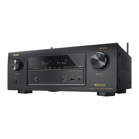
INTEGRATED NETWORK AV RECEIVER
AVR-X3400H
• For purposes of improvement, specifications and design are subject to change without notice.
• Please use this service manual with referring to the operating instructions without fail.
• Some illustrations using in this service manual are slightly different from the actual set.
Service Manual
Click here!
On-line service parts list
http://dmedia.dmglobal.com/Document/DocumentDetails/23186
Online Parts List
(P5 to P7)
WEB owner's manual
http://manuals.denon.com/AVRX3400H/NA/EN/index.php (May 2017)
http://manuals.denon.com/AVRX3400H/EU/EN/index.php (June 2017)
http://manuals.denon.com/AVRX3400H/AP/ZH/index.php (August 2017)
CAUTION IN SERVICING
ELECTRICAL
MECHANICAL
REPAIR INFORMATION
UPDATING
Please refer to the MODIFICATION NOTICE.
Ver. 2
(Release schedule)
Advertisement

Related Manuals for Denon AVR-X3400H


Summary of Contents for Denon AVR-X3400H
- Page 1 INTEGRATED NETWORK AV RECEIVER Click here! AVR-X3400H On-line service parts list http://dmedia.dmglobal.com/Document/DocumentDetails/23186 Online Parts List (P5 to P7) WEB owner’s manual (Release schedule) http://manuals.denon.com/AVRX3400H/NA/EN/index.php (May 2017) http://manuals.denon.com/AVRX3400H/EU/EN/index.php (June 2017) http://manuals.denon.com/AVRX3400H/AP/ZH/index.php (August 2017) CAUTION IN SERVICING ELECTRICAL MECHANICAL REPAIR INFORMATION UPDATING • For purposes of improvement, specifications and design are subject to change without notice.
- Page 2 CAUTION IN SERVICING SAFETY PRECAUTIONS NOTE FOR SCHEMATIC DIAGRAM NOTE FOR PARTS LIST INSTRUCTIONS FOR HANDLING SEMICONDUCTORS AND OPTICAL UNIT Online Parts List Accessing the Parts List Logging in to New SDI and Accessing the Parts List Accessing the Part List from the Model Asset Screen PRINTED CIRCUIT BOARDS Parts Table Downloading the Parts List as an Excel File Revision History...
- Page 3 SAFETY PRECAUTIONS ◎ Make a safety check after servicing! The following items should be checked for continued protection of the customer and the service Check that all screws, parts and wires removed or disconnected when servicing have been put back technician.
- Page 4 NOTE FOR SCHEMATIC DIAGRAM WARNING: Parts indicated by the z mark have critical characteristics. Use ONLY replacement parts recommended by the manufacturer. CAUTION: Before returning the set to the customer, be sure to carry out either (1) a leakage current check or (2) a line to chassis resistance check.
- Page 5 Online Parts List Accessing the Parts List Logging in to New SDI and Accessing the Parts List (1) Click the URL link on the cover of the service manual. (1) Access New SDI from the URL below. Examples of display <http://dmedia.dmglobal.com>...
- Page 6 Accessing the Part List from the Model Asset Screen Downloading the Parts List as an Excel File (1) Display Model Asset from New SDI. (1) Displays the Parts List. Click the Download icon. (2) Click the section displayed as ▼ Link to Part Lists under the model name. NOTE : If the ▼...
- Page 7 Searching Part Numbers or Ref. Numbers You can search a Parts List for part numbers or Ref. numbers. (1) Enter the part number or Ref. number in the search window of the Parts List, and press the search button. (2) The search results are displayed. The name of the sheet in which the search part is used and the part’s line are displayed.
- Page 8 CAUTION IN SERVICING. Initializing This Unit Make sure to initialize this unit after replacing the microcomputer or any peripheral equipment, or the digital PCB. 1. Press the power button to turn off the power. 2. While holding down buttons "ZONE2 SOURCE" and "DIMMER" simultaneously, press the power but- ton to turn on the power.
- Page 9 ELECTRICAL SCHEMATIC DIAGRAMS PRINTED CIRCUIT BOARDS SCH01_HDMI SW2 DIGITAL, F HDMI SCH02_HDMI SW1 INPUT, VIDEO, FRONT CNT SCH03_NET PHY SCH04_CPU LEVEL CHG MAIN, RS CNT, GUIDE L、FH GUIDE SCH05_DIGITAL CNT FRONT, CNT, RS232, FUNCTION, TOP GUIDE SCH06_CPU SMPS SCH07_DSP SCH08_ADV8003 LEVEL DIAGRAM SCH09_ADV8003 DDR FRONT ch...
- Page 10 SCHEMATIC DIAGRAMS SCH01_HDMI SW2 HDMI SW2 N1001 A111989-A-01-T R1017 RX1_5V HP_DET Q1000 HPD1 RT1N141C STBY5V DDC_SDA Q1001 FROM RT1N441C CEC5V DDC_SCK D.SUPPLY R1019 CEC3.3V RX1_DDCDA L1000 CB05YTYH221 CE_REMOTE R1021 CEC1.1V2 RX1_DDCCL L1016 TXC- DGND TO 0A RX1_C- CB05YTYH221 TXC_SHLD TXC+ RX1_C+ TX0- RX1_0-...
- Page 11 SCH02_HDMI SW1 HDMI SW1 FROM CEC5V_1 D.SUPPLY CEC3.3V L1007 CB05YTYH221 CEC1.1V1 L1019 P1_C- DGND TO 5A CB05YTYH221 P1_C+ P1_D0- P1_D0+ FROM P1_D1- P1_D1+ HDMI SW2 P1_D2- L1008 FBMJ3216HL160NT P1_D2+ TO A2 L1009 CB05YTYH221 N1005 A111989-A-01-T C1233 10U-K-2012(OPEN) AVDD11RX_1 R1125 AVDD11RX_1 RX5_5V AVDD33RX_1 HP_DET...
- Page 12 SCH03_NET PHY TO 1B TO 2B FROM NET PHY TO CPU DIGITAL_CNT NET_I2S2_DOUT NET_I2S2_BCKIN NET_I2S2_DIN NET_I2S2_LRCKIN R1322 NET_I2S0_DOUT. R1321 NET_I2S_BCLKOUT. NET_TDM_DOUT R1320 NET_I2S_LRCKOUT. NET_TDM_BCKIN NET_TDM_FSIN NET3.3V FROM LEGO5V D.SUPPLY DGND 19 18 17 TO 3B DIR/A.PLD TO 9A 9 10 R1207 R1208 NET_I2S0_DOUT...
- Page 13 SCH04_CPU LEVEL CHG CPU LEVEL CHG TO DIGITAL CNT TO 8B SWM3.3V FROM M3.3V D.SUPPLY DGND TO 9B SWM3.3V DGND TO CPU TO 0C GND LINE POWER+ LINE POWER- LINE ANALOG AUDIO DIGITAL AUDIO TMDS SIGNAL ANALOG VIDEO DIGITAL VIDEO STBY POWER...
- Page 14 SCH05_DIGITAL CNT TO 1C DIGITAL CNT TO D.SUPPLY DA+5V N1018 MUTE3.3V N1018 TO CP1018 C125Z2-21C DAGND DAC_FL- DAC_FL+ CN1040 DAGND DAGND DAC_FR+ DAC_FR- DAGND DAGND N1040 C125Z2-31C CEN- DAC_C- CEN+ DAC_C+ VOL_CLK MVOL_CLK DAGND DAGND VOL_DATA MVOL_DATA DAC_SL- MVOL_MUTE MVOL_MUTE DAC_SL+ ZVOL_CLK ZVOL_CLK...
- Page 15 SCH06_CPU TO 4C TO 5C TO 6C TO C0 TO 7C TO B1 TO CPU LEVEL CHG NET PHY ADV7180 TO ADV8003 TO D.SUPPLY C1356 OPEN DSP1CLK CEC_COM CEC_COM DSP1MISO H5VDET R1488 DSP1MOSI Q1043 HINSELC DSP1RST 2SD2114K HINSELB R1490 DSP1CS HINSELA 100K DSP1FLAG0...
- Page 16 SCH07_DSP TO 3D TO C8 TO DIR/A.PLD TO CPU MP OPEN N1034 1.0-16-6PB-2 DSP1CS DSP1MISO DSP1MOSI DSP1CLK DGND DA3.3V L1129 CB05YTYH221 L1130 CB05YTYH221 DSP1MISO DSP1CLK DSP1MOSI DSP1CS R2181 10K*4(AR) R1649 OPEN R1653 R1654 R1655 OPEN R1837 C1429 1N-K U1023 C1430 1N-K W9864G6KH-5 C1432...
- Page 17 SCH08_ADV8003 ADV8003 DV5V FROM DV3.3V D.SUPPLY DV1.8V DGND DVDD_TX AVDD3_1_TX PVDD_TX PVDD3_TX PVDD5_TX AVDD2_TX L1041 L1038 L1039 L1040 L1042 L1043 CB05YTYH221 CB05YTYH101 CB05YTYH221 CB05YTYH221 CB05YTYH221 CB05YTYH221 TO 4D DDR_1.8V PVDDR_TX AVDD3_3_TX AVDD3_2_TX CVDD1 PVDD6_TX DVDDIO_TX L1045 L1044 L1046 L1047 L1048 L1049 CB05YTYH221 CB05YTYH221...
- Page 18 SCH09_ADV8003 DDR ADV8003 DDR TO D7 TO D8 TO D9 ADV8003 ADV8003 ADV8003 U1028 A3R12E40DBF-8E(512Mb) U1029 A3R12E40DBF-8E(512Mb) DDR2 DDR1 DDR_1.8V DDR_1.8V DGND DGND DR_TXDQSB1 DDR_1.8V DDR_1.8V DGND DGND DR_TXDQSB3 DDR_1.8V DR_TXDQ14 DGND DR_TXDM1 DR_TXDQS1 DGND DR_TXDQ15 DR_TXDQ30 DGND DR_TXDM3 DR_TXDQS3 DGND DR_TXDQ31 DDR_1.8V...
- Page 19 SCH10_D.SUPPY L1054 CB05YTYH221 D.SUPPLY L1055 CB05YTYH221 OPEN L1056 CB05YTYH221 R1814 0(OPEN) STBY5V N1033 R1813 0(OPEN) TO A0 1.117V CEC5V OPEN N1033 L1020 L1133 1.5A CEC3.3V 2.2UH 0-2012 YMW025-06R CEC1.1V2 CEC1.1V2 U2806 L1134 NCP380HMUAJAATBG(OPEN) R1050 DGND RESETOUT CEC_POWER 0-2012 R1812 2R7-1608 D5.2V D5.2V R1809...
- Page 20 SCH11_HDMI TX HDMI TX VDD33IO CEC5V CEC3.3V CEC1.1V L1088 FBMJ3216HL160NT DGND L1087 PVDD33 L1115 FBMJ3216HL160NT L1086 CB05YTYH221 CB05YTYH221 TO E2 U1032 AP7361-ADJ L1083 CB05YTYH221 AVDDH33 L1082 CB05YTYH221 AVDD11 L1140 CB05YTYH221 C2245 2.2U-K-1608 R2156 VDD33 L1084 CB05YTYH221 R2157 OPEN R2155 VDD11 L1085 CB05YTYH221 R2158...
- Page 21 SCH12_DIR A.PLD TO A8 TO B0 TO A9 TO E4 TO E5 TO 7E TO C9 TO VIDEO PLD DIR/A.PLD FROM NET PHY FROM HDMI TX TO HDMI TX FROM HDMI SW1 TO CPU FROM NET PHY *FILTER COMPONENTS VALUE TYPE TOLERANCE R1907...
- Page 22 SCH13_MAIN DAC TO E8 TO F1 TO D0 TO F0 TO E9 MAIN DAC FROM FROM FROM FROM FROM DIR/A.PLD DIR/A.PLD DIR/A.PLD DIR/A.PLD ADIN_LEGO_L DAGND ADIN_LEGO_R DAGND A/DIN_R DAGND A/DIN_L C2187 100N-K-1608 DACRTNGND C2188 100N-K-1608 DA+5V A/DIN_L A/DIN_R DA+5V C2137 R1999 DAGND 100-1608...
- Page 23 SCH14_VIDEO_PLD TO E6 TO/FROM HDMI TX VIDEO PLD DOPI_PCK DOPI_PCK DOPI_D0 DOPI_D0 DOPI_D1 DOPI_D1 DOPI_D2 DOPI_D2 U1011 DOPI_D3 DOPI_D3 EPM570F256C4N DOPI_D4 DOPI_D4 DOPI_D5 DOPI_D5 DOPI_D6 DOPI_D6 DOPI_D7 DOPI_D7 R2189 8KOPI_Y11/R7 8KOPI_Y11/R7. 10*4(AR) TO 2F DGND 8KOPI_C2/B2 DV3.3V PO8KI_Y9/R5 PO8KI_Y5/R1_PLD PO8KI_Y4/R0 PO8KI_Y3/G7_PLD PO8KI_Y2/G6_PLD POHI_HSYNC.
- Page 24 SCH15_ADV7180 ADV7180 L1034 CBC2518T220M L1033 CBC2518T220M L1032 CB05YTYH221 DV1.8V L1031 CB05YTYH221 DV3.3V DGND CEC3.3V X1019 TO E0 28.63636MHz(7P) C2218 10N-K C2217 R2263 82N-K 1K69-F R2261 R2273 OPEN R2126 DOPI_PCK DECIN_V. R2264 C2211 10N-K C2210 100N-K C2421 OPEN U2022 DVDDIO ADV7180 R2089 36-1608 C2203...
- Page 25 SCH16_INPUT1 CN4201 CN4204 CN4203 CN4200 TO CP4206 TO CP4205 TO CP4203 TO CP401 FRONT_CNT 2/2 _ L7 SIDE_CNT 1/1 _ H7 SIDE_CNT 1/1 _ H7 INPUT 1/3 7CH_AMP TO 3F CN4201 CN4204 INPUT 2/3 R4201 C4277 C125Z2-27C C125Z2-09C CN4200 9 10 11 12 13 WIRE_13P CN4203 SAT_L...
- Page 26 SCH17_INPUT2 INPUT 2/3 CN4202 TO CP4202 SIDE_CNT 1/1 _ D7 CN4202 C125Z2-21C A+8V A-8V C4215 C4220 C4218 OPEN C4222 OPEN 220/25(KR3) 220/25(KR3) U4200:A R4203 R4204 C4210 NJM8080G 3.9K-F (CH)3900P-J R4207 R4210 DA_FL. DA_FL. C4211 INPUT 2/3 R4209 100/50(KR3) DA_FR. 3.9K-F C4217 (CH)680P-J DA_C.
- Page 27 SCH18_F.HDMI INPUT 3/3 R1552 R1546 R1547 R1549 1K-1005 10K-1005 47K-1005 OPEN-1005 R1548 OPEN-1005 N1026 A0D7ABAR19N0 R1551 OPEN-1005 Q1046 RT1N141C F.HPA_D.. HP_DET Q1047 RT1N441C N1038 DDC_SDA DDC_SCK N1038 6232-23P(KYOCERA) CE_REMOTE F.CEC TXC- F.CEC R1550 R1533 HPDF TXC_SHLD 0-1005 0-1005 F.HPA_D.. TX_EN TXC+ DDCA_SDA TX0-...
- Page 28 SCH19_VIDEO VIDEO_F/CNT 1/2 VIDEO PART CVBS INPUT SW NJM2595MTE1 INPUT OUT PUT AVR-X3400 SW4 SW5 JACK5004 MUTE MUTE VIN 3 CBL/SAT GAME GAME VIN 4 C5028 VIN 5 GAME 10/50 IC5001 NJM2595M R5012 OPEN V+5V V+5V CN5000 R5008 C5026 VIDEO_F/CNT 2/2 _ F4 VIN5 10/50 VIN1...
- Page 29 SCH20_FRONT_CNT VIDEO_F/CNT 2/2 FRONT_CNT PART CP1039 HDMI _ DIGITAL CNT _ D5 TO CN1040 CP1039 C125Z1-31 FUSE F5006,F5007,F5008,F5009 F5005 AVR-X3400 T1.6AL/250V T1.25AL/250V CP5000 CP5000 BKT5004 C125Z1-21 F5005A F5005B T1.25AL 250V F5005 TRG_15V_A C5046 OPEN MAIN TRANS TAP CP5003 F5006 YMAW025-08R T1.6AL 250V F5006A F5006B...
- Page 30 SCH21_AMP1 PAGE 1 AVR-X3400 AMP SCH AMP B'D 1/2 56.8V 61.2V R401 R703 ZD401 R402 R403 60.4V R405 R404 R406 ZJ5.1A 100K 270(1) C401 270(1) OPEN CP501 DHPTF1608 471P 115T C402 100N-K Q401 56.1V D401 OPEN SC52136-021A C403 R407 KTA1024Y 1N4148 10N-K 0.6V...
- Page 31 SCH22_AMP2 TO F4 TO F5 PAGE 2 PAGE 2 PAGE 2 AMP B'D 1/2_A10 AMP B'D 1/2_M10 R706 R531 R532 ZD410 R533 R535 R534 100K R537 ZJ5.1A 270(1) CP504 270(1) OPEN C449 DHPTF1608 471P 115T C450 Q437 SC52136-021A D419 OPEN 100N-K KTA1024Y 1N4148...
- Page 32 SCH23_SPK MAIN 1/3 SPK PART R4000 470(2) H/PR R4016 L4000 OPTION M SP-2507 D4000 RLY4000 OPTION O LBAS16HT1G OPTION N C4000 HFD27/012-S 47N-100V(PEF) C4003 R4002 OPEN R4003 R4001 470(2) JACK4000 H/PL 10(2) FR_GND C4001 C4002 22N-100V(PPF) OPEN R4017 FR_A L4001 SP-2507 FL_GND C4004...
- Page 33 SCH24_REG SPK PART A8 MAIN 2/3 TO F6 TUNER / REG PART X2400/SR5012 : VIDEO_F/CNT 2/3 _ J9 X3400 : VIDEO_F/CNT 2/2 _ J9 A_-8V CP4003 CP4003 A_+8V C125Z1-19 OPTION A HDAM_GND HDAM_GND D4010 D4009 H/PL H/P_L 1N4007S 1N4007S TRG_15V TRG_15V H/P_GND H/P_GND...
- Page 34 SCH25_RS CNT MAIN 3/3 RS_CNT PART (AVR_X2400E3_X3400_SR5012 ONLY) SR5012 ONLY CP4700 X2400/SR5012 : INPUT 1/1 C1 X3400 : SIDE CNT 1/1 _ L1 TO CN4700 R1452 C1341 OPEN D1094 C1342 4.7U-K-1608 LBAS16HT1G C1343 OPEN U1019 R94EV1A Q1037 CP4700 OUTPUT RT1P141C D1095 C125Z1-07,13,15 AVR_X2400E3 : 7P...
- Page 35 SCH26_FRONT FRONT 1/2 AVR_S930_X2400_X3400 FRONT MODEL AVR S930 AVR X2400 AVR X3400 AREA E2/E1C/K E2/E1C OPTION A OPTION_C R4440 OPEN OPEN FL4400 R4441 OPEN OPEN OPEN 018BT021GINK R4462 1.2K 1.2K AVR-S930 / X2400 AVR-X3400 R4463 1.2K 1.2K OPTION C 018BT021GINK CIG25-1801N FL4400 TUNED...
- Page 36 SCH27_RS232 FRONT 2/2 RS232 PART (AVR_X2400E3_X3400 ONLY) AVR-X3400 ONLY U4700 PQ120DNA TRG_15V TRIGGER ON/OFF JACK4700 ZD4700 C4704 PJ-308-02(RD) ZJ16B 100N-K C4705 TRG_GND 100N-K D4703 LBAS16HT1G TRG1 10/50 C4706 100N-K C4707 C4712 100N-K C4711 D4701 OPEN R4708 100N-K T1 OUT C4716 R1 IN 100N-K R4709...
- Page 37 SCH28_SIDE_CNT SIDE_CNT 1/1 CN4700 TO CP4700 MAIN 3/3 _ G2 CN4700 C125Z2-13 CP1018 CP1017 TO N1018 HDMI _ DIGITAL CNT _ H5 CP1023 TO N1023 HDMI _ DIGITAL CNT _ H3 TO N1022 HDMI _ DIGITAL CNT _ N5 CP1018 CP1017 CP1023 C125Z1-31...
- Page 38 SCH29_SMPS AVR-X3400 SMPS OPTION BK901 AC100-120V:T2AL 250V M3_BURRING AC220-240V:T1.6AL 250V D9002 1N4007 LF901 J9008 OPTION OPTION F9001B F9001A LIVE SQ2424 29mH D9001 1N4007 C3A206 F9001 C9002 0.01UF/250V Neutral R9008 ¡Ü JK901 ZD911 C9012 ¡Ü D9003 1N4007 ZD908 YW396-03AV 2200PF/1KV-3225 P6KE150A D9012 P6KE120A R9009...
- Page 39 PRINTED CIRCUIT BOARDS DIGITAL, F HDMI Lead-free Solder When soldering, use the Lead-free Solder (Sn-Ag-Cu). DIGITAL (A SIDE) F HDMI (A SIDE) F HDMI (B SIDE) BKT1000 C1320 C1319 C1317 R1999 R2010 R2021 R2044 R2058 R2069 R2082 N1017 R2002 R2013 R2017 R2047 R2062...
- Page 40 INPUT, VIDEO, FRONT CNT INPUT (A SIDE) INPUT (B SIDE) FRONT CNT (A SIDE) FRONT CNT (B SIDE) R4296 C4261 R4291 R4356 R4309 R4209 C4210 R4203 C4292 R4352 R4493 D4203 R4217 D4202 NC(HDAM_GND) NC(HDAM_GND) C4216 R4476 H/P_L R4207 R4354 C4279 C4217 C4297 C4296...
- Page 41 AMP (A SIDE) G403 7CH AMP B'D MP CLAMP 402 BAR CODE WIRE J590 G400 G401 C408 7020-08117-000-0S WIRE G401 G402 WIRE BONDING CLAMP 401 CP401 BONDING BONDING R687 JW595 JW596 C533 C456 C424 CLAMP 400 R472 C528 R428 R558 VR404 C440 C472...
- Page 42 MAIN, RS CNT, GUIDE L、FH GUIDE MAIN (A SIDE) MAIN (B SIDE) R4067 NJM4580CG R4050 U4005 R4063 R4058 D4043 HDAM_GND HDAM_GND H/P_L H/P_GND H/P_R R4054 RLY_F RLY_C/S RLY_SB RLY_H/P RLY_HIB R4057 DGND R4055 AMPSIG_DET CURRENT_DET V-5V V-5V VAGND VAGND V+5V V+5V C4071 R4044...
- Page 43 FRONT, CNT, RS232, FUNCTION, TOP GUIDE FRONT (A SIDE) FRONT (B SIDE) CNT (A SIDE) CNT (B SIDE) CNT B'D(MP) CNT B'D(MP) 7020-08113-000-0S 7020-08113-000-0S C4441 C4478 C4477 M3.3V D/MGND SWM3.3V A+7V A-7V MICGND V.AUX/GND H/PGND H/PL H/PR FRONT_IRIN SWM5V RS232C (A SIDE) RS232C (B SIDE) POWERKEY REDLED...
- Page 44 SMPS SIDE CNT (A SIDE) SIDE CNT (B SIDE) SMPS (A SIDE) SMPS (B SIDE) BK902 CY901 CY902 BK901 Sec. 470PF/400V 470PF/400V CLP4000 Sec. CLP4002 CLP4001 JK901 Pri. Pri. Sec. Sec. Pri. NEUTRAL(W) LIVE(B) Pri. J9006 Sec. AC100_120V:T2AL/250V J9007 Sec. AC220_240V:T1.6AL/250V F9001 CX901...
- Page 45 LEVEL DIAGRAM FRONT ch AVR-X3400H LEVEL DIAGRAM FRONT ch NJU72750 NJU72343 ANALOG H/POUT SPEAKER LINE IN + GAIN ADJ. AK4458VN AK5358B + + PREOUT - - to ZONE2 +30dB NJU72343 MAX. OUTPUT 4.2Vrms SP OUT Differential Out 4.48Vrms/8Ω AK4458 MAX SIGNAL LEVEL...
- Page 46 CENTER, SURROUND, SURR.BCK ch AVR-X3400H LEVEL DIAGRAM CENTER ch SURROUND ch SURR.BCK ch NJU72343 SPEAKER + GAIN ADJ. AK4458VN + + PREOUT - - +30dB NJU72343 MAX. OUTPUT 4.2Vrms SP OUT Differential Out 4.23Vrms/8Ω AK4458 MAX SIGNAL LEVEL 0dBFS +20dB DOLBY LIMIT LEVEL (ALLch-3dBFS) 0dBFS = +/-2.8Vpp=1.98Vrms...
- Page 47 SUBWOOFER ch AVR-X3400H LEVEL DIAGRAM SUBWOOFER ch NJU72343 GAIN ADJ. AK4458VN + + PREOUT - - NJU72343 MAX. OUTPUT 4.2Vrms +30dB MAX SIGNAL LEVEL DOLBY LIMIT LEVEL (ALLch-3dBFS) 0dBFS = +/-2.8Vpp=1.98Vrms AK4458 0dBFS +20dB -10dBFS +10dB PREOUT 300mVrms -20dBFS PREOUT 150mVrms -2.0-0.5+14=11.5dB...
- Page 48 ZONE2 ch AVR-X3400H LEVEL DIAGRAM ZONE2 NJU72750 NJU72343 from To MAIN LINE IN DA SB-ch + SPEAKER ZONE GAIN NJU72343 NJW1194 NJU72750 TONE ZONE2 MONO MONO GAIN MONO PCM5100 +30dB NJU72343 MAX. OUTPUT 4.2Vrms SP OUT PCM5100 4.23Vrms/8Ω 0dBFS = 2.0Vrms...
- Page 49 ZONE2(LEGO) ch AVR-X3400H LEVEL DIAGRAM ZONE2(LEGO) NJU72750 LINE IN To MAIN To ZONE2 PCM9211 To LEGO +30dB +20dB +20dB PCM9211 0dBFS=1.06Vrms +10dB +10dB -10dBFS LINE IN 200mV -8.5dB -20dBFS A/D IN -10dB -10dB 75.2mVrms (-23.0dBFS) -30dBFS -20dB -20dB -40dBFS -30dB...
- Page 50 BLOCK DIAGRAM ANALOG AUDIO DIAGRAM AVR_X3400 ANALOG AUDIO DIAGRAM TO DIGTAL AUDIO BLOCK 7-INPUT/3-OUT NJU72750 8-CH VOLUME NJU72343 7-INPUT/3-OUTPUT NJU72750 InA1 CBL/SAT_L 8-CH VOLUME InA2 NJU72343 DVD_L InA3 OutA1 MAIN_AD_IN_L MAIN_L InA1 OutA Blu-ray_L DA_FL InA4 OutA2 LEGO_L GAME_L InA2 InA5 OutA3 ZONE2_L...
- Page 51 DIGITAL AUDIO DIAGRAM AVR_X3400 DIGITAL AUDIO DIAGRAM TMDS HDMI ZONE2 AD8195 FRONT TMDS TMDS IN_3 HDMI BUFFER TMDS HDMI OUT1 OUT_1 27MHz TMDS MN864787 HDMI OUT2 TMDS TMDS OUT_0 OUT_0 IN_1 IN_3 HDMI1 MN864788 HDMI (TX / RX / OSD / Scaler ) TMDS IN_0 HDMI2.0...
- Page 52 VIDEO DIAGRAM AVR_X3400 VIDEO DIAGRAM TMDS HDMI ZONE2 AD8195 FRONT TMDS TMDS HDMI OUT1 IN_3 TMDS OUT_1 HDMI BUFFER 27MHz HDMI OUT2 TMDS OUT_0 MN864787 HDMI (TX / RX / OSD / Scaler ) TMDS TMDS IN_3 OUT_0 IN_1 HDMI1 (1080p ->...
- Page 53 POWER DIAGRAM AVR-X3400 VCC DIAGRAM MAIN +B S1(AMP +B) MAIN -B +3.3V ( PCM5100A*2 ) AP7361-ADJ DA+5.0V ( AK4458VN / AK5358BET / PCM9211 ) KIA7805API A+7.0V KIA7808API A-7.0V KIA7908PI S2(+8V,-8V) TRIGGER +12V PQ120DNA A.V+5.0V KIA7805API JUMPER TUNER_+5V RELAY MAIN TRANS KIA7905PI A.V-5.0V FL AC (F1)
- Page 54 WIRING DIAGRAM AVR_X3400 WIRE DIAGRAM DIGITAL PCB MAIN PCB NETWORK MODULE FRONT CNT PCB VIDEO PCB INPUT PCB 7CH AMP PCB VOLUME PCB FRONT PCB FUNCTION PCB H/P PCB USB PCB...
- Page 55 SEMICONDUCTORS Only major semiconductors are shown, general semiconductors etc. are omitted to list. The semiconductor which described a detailed drawing in a schematic diagram are omitted to list. 1. IC's R5F564MJCDFC (DIGITAL : U1018) Pin Name Symbol Pu/Pd STBY STOP Function STBY Smoothing capacitor connection pin...
- Page 56 Pin Name Symbol Pu/Pd STBY STOP Function Pin Name Symbol Pu/Pd STBY STOP Function STBY STBY V.PLD_ APLD_CS Audio PLD (5M570ZF256C5N) control pin P87/TXD10/TIOCA2 Video PLD control pin (for setting of GUI transmittance) TRANS2 APLD_DATA/ Audio PLD (5M570ZF256C5N) control pin/DAC PB3/SCK4/SCK6 P16/TXD1/RXD3/ NET5V_POW-...
- Page 57 AD8195 AD8195ACPZ (INPUT : U1022) Pin Name Symbol Pu/Pd STBY STOP Function STBY PIN CONFIGURATION AND FUNCTION DESCRIPTIONS PD7/IRQ7/AN107 DIR_CE DIR (PCM9211) control pin DIR_DOUT DA3.3Pu DIR (PCM9211) control pin PD6/IRQ6/AN106 DIR_CLK DIR (PCM9211) control pin DIR_RST DIR (PCM9211) control pin 30 AVCC PD5/IRQ5/AN113 787_HAINT...
- Page 58 PCM9211 www.ti.com SBAS495 – JUNE 2010 PIN CONFIGURATIONS PCM9211 (DIGITAL : U1040) PT PACKAGE LQFP-48 DESCRIPTION (TOP VIEW) NAME TOLERANT 26 MS/ADR1 Software control I/F, SPI chip select / I2C slave address setting1(2) ERROR/INT0 VDDRX 27 MODE Control mode setting, (see the Serial Control Mode section, NPCM/INT1 RXIN1 MPIO_A0...
- Page 59 PCM9211 LC89091JA (DIGITAL : U1004) PCM9211 BLOCK DIAGRAM www.ti.com SBAS495 – JUNE 2010 BLOCK DIAGRAM FILT LC89091JA AUXIN 0 AUTO RXIN7 RXIN 0 RXIN0 SCKO DOUT RXIN 1 RXIN1 MAIN OUTPUT RXIN 2 RXIN2 AUXIN0 LRCK SCKO/ BCK/LRCK PORT RXIN 3 RXIN3 AUXIN1 DOUT...
- Page 60 CS49844A (DIGITAL : U1073) W9864G6KH-5 (DIGITAL : U1023) SD_A3, EXT_A3, DAO3_D3, XMTA, GPIO113 SD_A2, EXT_A2 SD_D11, EXT_D3 SD_A1, EXT_A1 SD_D12, EXT_D4 SD_A0, EXT_A0 SD_D13, EXT_D5 SD_A10, EXT_A12 GNDIO4 SD_BA0, EXT_A13 VDDIO4 SD_BA1, EXT_A14 SD_D14, EXT_D6 W9864G6KH SD_CS, EXT_OE SD_D15, EXT_D7 SD_RAS, EXT_CS1 SD_D0, EXT_D8 SD_CAS, EXT_CS2...
- Page 61 AK4458VN 40 +105 C (Exposed pad is connected to ground) 40 +85 C (Exposed pad is open) 48-pin QFN (0.5mm pitch) AKD4458 Evaluation Board for AK4458 AK4458VN (DIGITAL : U1051) W9864G6KH-5 Block diagram Pin Configurations CLOCK BUFFER CONTROL SIGNAL GENER ATOR COMMAND DECODER COLUMN DECODER...
- Page 62 [AK4458] FUNCTIONAL BLOCK DIAGRAM No. Pin Name I/O Function PD State 4. Block Diagram and Functions CAD0_I2C Chip Address 0 Pin in I2C Bus serial control mode Chip Select Pin in 3-wire serial control mode LDOE TVDD VDD18 DVSS AVDD AVSS Hi-Z Audio Data Format Select in Parallel control mode.
- Page 63 SLAS764 – MAY 2011 www.ti.com DEVICE INFORMATION PCM5100 (DIGITAL : U1052, U1053, U1054) NJU72343 (INPUT : IC4202, IC4203) TERMINAL FUNCTIONS, PCM510x PCM510X (top view) Pin Function No. Symbol Function No. Symbol Function AREF Analog reference potential terminal DATA IC control data input Address selection terminal CLOCK IC control clock input...
- Page 64 G Bipolar Technology G Package Outline GENERAL DESCRIPTION DIP16,DMP16 PACKAGE OUTLINE The NJM2586A is a wide band 3-input 1-output 3-circuit video I PIN CONFIGURATION and BLOCK DIAGRAM amplifier. It is suitable for Y, Pb, and Pr signal because frequency NJM2595MTE1 (VIDEO:IC5001) range is 50MHz.The NJM2586A is suitable for AV receiver, STB, and other high quality AV systems.
- Page 65 ANODE CONNECTION 2. FL DISPLAY 17G(AD3) 18G(AD4) FLD (018BT021GINK) (FRONT : FL4400) 8G 9G 10G 11G 12G 13G 14G 15G 16G PIN CONNECTION NOTE 1) F1, F2 ----Filament 2) NP ------No pin 3) DL ------Datum Line 4) NX ------No extend pin 5) LGND ----Logic GND pin 6) PGND ----Power GND pin 7) VH...
- Page 66 3. Remote Code Table FORMAT SHARP FORMAT: SHARP / DATA CONSTRUCTION 15bits C14 0 C15 0=NOT INVERTED, 1=INVERTED /REMOTE ID : 1 FORMAT: SHARP / DATA CONSTRUCTION 15bits C14 0 C15 0=NOT INVERTED, 1=INVERTED /REMOTE ID : 1 SYSTEM ADDRESS(C1~C5) : 00110 , EXTENSION BIT (C12,C13) : 01 SYSTEM ADDRESS(C1~C5) : 01000...
- Page 67 FORMAT: SHARP / DATA CONSTRUCTION 15bits C14 0 C15 0=NOT INVERTED, 1=INVERTED /REMOTE ID : 1 FORMAT: SHARP / DATA CONSTRUCTION 15bits C14 0 C15 0=NOT INVERTED, 1=INVERTED /REMOTE ID : 1 SYSTEM ADDRESS(C1~C5) : 00110 , EXTENSION BIT (C12,C13) : 10 SYSTEM ADDRESS (C1~C5) : 01000...
- Page 68 RCSHP0420027 110110 MAIN ZONE 001100 001110 RCSHP0420012 RCSHP0420028 REMOTE ID SET: 1 RCSHP0420013 101100 RCSHP0420029 101110 MultEQ XT DENON CODE Parity GENRE1 GENRE2 RCSHP0420014 011100 RCSHP0420030 011110 4 5 2 3 0 9 10 11 12 13 14 15 16...
- Page 69 RCKSK0410030 CURSOR RIGHT RCKSK0410437 SDL LEVEL UP RCKSK0410031 ENTER RCKSK0410438 SDL LEVEL DOWN RCKSK0410439 SDR LEVEL UP RCKSK0410034 RETURN/BACK RCKSK0410440 SDR LEVEL DOWN RCKSK0410035 SETUP MENU RCKSK0410036 MEMORY RCKSK0410522 FRONT SPEAKER RCKSK0410542 DYNAMIC VOLUME OFF RCKSK0410042 UPGRADE ID ON RCKSK0410545 DYNAMIC VOLUME SELECT RCKSK0410045 Bilingual Mode(toggle) (JP only)
- Page 70 ZONE2 Bluetooth ZONE2 RCKSK0430764 ZONE2 Spotify (NA & EU only) RCKSK0430765 ZONE2 Pandora (NA only) REMOTE ID SET: 1 RCKSK0430787 ZONE2 INPUT SOURCE SELECT Right DENON CODE Parity GENRE1 GENRE2 RCKSK0430788 ZONE2 INPUT SOURCE SELECT Left RCKSK0430788 ZONE2 SLEEP 4...
- Page 71 ANALOG TUNER HEOS MUSIC REMOTE ID SET: 1 REMOTE ID SET: 1 DENON CODE Parity GENRE1 GENRE2 DENON CODE Parity GENRE1 GENRE2 4 5 2 3 0 4 5 2 3 0 25 26 27 28 25 26 27 28...
- Page 72 MECHANICAL DISASSEMBLY Flowchart 1. WiFi ANT 2. FRONT PANEL ASSY 3. RADIATOR ASSY 4. DIGITAL PCB 5. VIDEO PCB 6. INPUT PCB 7. MAIN PCB 8. SMPS PCB 9. TRANS EXPLODED VIEW PACKING VIEW...
- Page 73 DISASSEMBLY Flowchart • Remove each part following the flow below. • Reassemble the removed parts in the reverse order. • Read "SAFETY PRECAUTIONS" before reassembling the removed parts. • If wire bundles are removed or moved during adjustment or part replacement, reshape the wires after completing the work. Failure to shape the wires correctly may cause problems such as noise. •...
- Page 74 • The photographs with no shooting direction indicated were taken from the top of the unit. (1) Remove the screws. • Photos of AVR-X3400H E3 are used in this manual. The viewpoint of each photograph (Shooting direction : X) [View from the top] ↓Shooting direction: B↓...
- Page 75 3. RADIATOR ASSY 4. DIGITAL PCB Proceeding : TOP COVER → RADIATOR ASSY Proceeding : TOP COVER → WiFi ANT → DIGITAL PCB (1) Remove the screws. (1) Remove the screws. ↓Shooting direction: D↓ ↓Shooting direction: C↓ View from the bottom (2) Cut the wire clamps, then remove the CORD HOLDERs and connectors.
- Page 76 5. VIDEO PCB 7. MAIN PCB Proceeding : TOP COVER → WiFi ANT → DIGITAL PCB → VIDEO PCB Proceeding : TOP COVER → WiFi ANT → DIGITAL PCB → VIDEO PCB → INPUT PCB → MAIN PCB (1) Remove the connector. (1) Remove the screws.
- Page 77 EXPLODED VIEW http://dmedia.dmglobal.com/Document/DocumentDetails/23186 Parts List : "PROCEDURE AFTER REPLACING THE U-COM, "1. WiFi ANT" ETC." E X2 P8-1 J X3 P13-2 K X3 P19-3 P13-1 P19-2 P13-4 P19-1 29 X2 P8-4 P13-3 P8-2 P8-3 P12-1 J X3 P12-3 P12-2 25X2 P12-1 P9-1 X2 A X1...
- Page 78 Notes on RADIO (ALL) SPOTIFY insertion sheet This part together with document and zipper bag are supplide. Cautions on Using Batteries (E2 only) HEOS insertion Sheet (DENON) MIC STAND ASSEMBLY INSTRUCTION SAFETY INST. (ALL) QUICK START GUIDE (ALL) *Getting started...
- Page 79 REPAIR INFORMATION TROUBLE SHOOTING SPECIAL MODE 1. POWER Special mode setting button 2. Analog video 1. Version Display Mode 3. HDMI/DVI 2. PANEL / REMOTE LOCK Selection Mode 4. AUDIO 3-1. Selecting the Mode for Service-related 5. Network / Bluetooth / USB 3-2.
- Page 80 TROUBLE SHOOTING 1. POWER 1.1. The unit does not power on 1.2. Fuse is blown The unit does not power on Blown fuse Check for short circuits between the Does the power indicator on the front panel flash Check the rectifier diode in the Does the power shut down after several seconds? Check for leaks and short circuits regulator output terminal and GND...
- Page 81 2. Analog video CVBS / COMPONENT / HDMI OUT NG Input CVBS / COMPONENT Input CVBS Input COMPONENT Input Function : CBL / SAT Function : CBL / SAT HDMI Check the input signal to the VIDEO DECODER. Can a signal be confirmed at the following To "A"...
- Page 82 Input Input CVBS COMPONENT Check the settings of each IC. Check the settings of each IC. Are the following voltages set? Are the following voltages set? DIGITAL PCB DIGITAL PCB faulty. DIGITAL PCB DIGITAL PCB faulty. [N1040 : 10pin] : Hi (3.3 V) [N1039 : 9pin] : Lo (0 V) [N1040 : 11pin] : Hi (3.3 V)
- Page 83 3.1. No picture or sound is output (HDMI to HDMI) No picture or sound is output. (8) When using a DENON Blu-ray/DVD player, is the "HDMI" indicator of the fluorescent display lit? Proceed to YES when using a Blu-ray/DVD player produced by other manufactures.
- Page 84 (15) Are a picture and sound output when a differ- The TV is faulty. ent TV is used? Check the unit. "HDMI "Rx/Tx" Failure Detection"...
- Page 85 4. AUDIO 4.1. AUDIO CHECK No audio output CHECK 1 INPUT SURROUND MODE SOURCE Check the ANALOG AUDIO BLOCK Audio output OK? ANALOG 2CH DIRECT ANALOG CHECK 2 INPUT SURROUND MODE SOURCE Check the DIGITAL AUDIO BLOCK Legacy Audio output OK? COAX or OPT (PCM or DolbyDigital or dts…) CHECK 3...
- Page 86 4.2. Power AMP (AMP PCB) 4.3. Analog audio When using the protection pass mode, do not connect speakers to the speaker terminals. No audio output. No audio output. Protection is activated. Is a voltage of ± 8 V supplied to INPUT PCB Repair the ±...
- Page 87 5. Network / Bluetooth / USB 5.1. Cannot connect to the network Check the connection environment The circuit of NET5V POWER Insert the LAN cable correctly and then turn on Can the output voltage (5V) to Is NET5V POWER [U1018 : 48pin Is the LAN cable correctly inserted? between [U1018-Q1077 : FET- the power again.
- Page 88 5.2. Cannot establish a Bluetooth connection Check the Bluetooth device being used Are the versions of the HEOS Version displayed in The Network Module software is faulty. Version Check Mode? Is the Bluetooth device compatible with the A2DP Use a device that is A2DP profile compatible. profile? The circuit of Network Module is faulty.
- Page 89 5.3. Cannot recognize the connected USB device 5.4. No picture or sound is output Check the USB device being used Checking the unit (If no picture is output) Are digital video signals(LEGOPCK, LEGOVS, The circuit around Network Module, [U1011 : Is a USB hub being used? Do not use a USB hub.
- Page 90 DIGITAL test point USB test point C1320 C1319 C1317 R1999 R2010 R2021 R2044 R2058 R2069 R2082 BKT1000 N1017 C1313 C1314 C1316 R2002 R2013 R2017 R2047 R2062 R2072 R2085 N1000 BKT1001 U1012 L1058 N1019 C1874 NET5V_POWER C1918 N1017 C1551 C1546 Q1074 R1696 R1717 C1327...
- Page 91 6. SMPS Operation waveform for each part DC 5V is not output. After primary side rectification Primary drain (Caution: High voltage, electric shock) (Caution: High voltage, electric shock) Replace the [IC901 : TOP268EG Is [IC901 : TOP268EG] damaged? and D9001 / D9002 / D9003 / D9002 1N4007 J9008...
- Page 92 AUDIO CHECK PATH : Digital Signal : Analog Signal HDMI BLOCK HDMI BLOCK CHECK6 HDMI HDMI SPEAKER OUTPUT HDMI INPUT OUTPUT CHECK5 INPUT PREOUT HDMI Tranceiver CHECK4 AVR Supported "HD AUDIO" OUTPUT HDMI Tranceiver MN864788 ARC INPUT MN864787 TNDS FRONT BUFFER HDMI AD8195...
- Page 93 HDMI "Rx/Tx" Failure Detection 1. Prior checking Check item(0). : Checking the HDMI connector Checking the condition of the HDMI pin (rear/front). There are deformed pins. Replace the HDMI connector. Check for deformed pins. None of the pins are deformed. Check by following the flow chart for "3.
- Page 94 2. Preparations for checking HDMI Switcher reception/transmission register 2-3. Device configuration method 2-1. Necessary devices PC settings : Execute the serial communication program, Termite.exe. Check the product settings. 2-a) Player with an HDMI terminal 2-b) TV with an HDMI terminal (* NOTE : Do not use a computer monitor.) After executing Termite.exe, click [Settings].
- Page 95 Click the [click to connect] button to start communication. When the settings are correct, the following message will be displayed in the window of After a connection is established successfully, the display of the button name will change as Termite. shown in Figure 4.
- Page 96 3. Starting detecting the point of failure Check item(1). (2-2) Display when an Error is not detected. Check the power supply status and communication status with the CPU of each device. Start in HDMI Diagnostics mode and follow the procedures below. 1 Auto Test Cancel the mode, and proceed to check item...
- Page 97 Check item(2). : Does a video signal come from HDMI ZONE2 Check item(4). Does a video signal come from HDMI OUT1 to OUT to TV correctly? TV correctly? HDMI IN ZONE2 OUT HDMI IN HDMI OUT1/2 Go to check item (45) (Switcher1 failure detection proce- dure) Go to...
- Page 98 3-1. Error Code H1-01 failure detection procedure Checking device. [U1001 : MN864787] Check the power supply voltage. (HDMI Tx) Checking the reset waveform. (HDMI Tx) Check item(6). Check the power supply voltage. : Check item(8). Checking the reset waveform : Check the waveform.
- Page 99 Check the I2C communication line. (HDMI Tx) Check item(9). Check the I2C communication line : Check the CPU. Is the "I2C" waveform of the TP near the HDMI SW1 [U1003] correct (like the one shown in the diagram) when the power is turned on? I2C(HSCL) I2C(HSDA)
- Page 100 3-2. Error Code H1-02 failure detection procedure Checking device. [U1003 : MN864788] Check the power supply voltage. (HDMI SW1) Checking the reset waveform. (HDMI SW1) Check item(11). Check the power supply voltage. : Check item(13). Checking the reset waveform : Check the waveform.
- Page 101 Check the I2C communication line. (HDMI SW1) Check item(14). Check the I2C communication line : Check the CPU. Is the "I2C" waveform of the TP near the HDMI SW1 [U1003] correct (like the one shown in the diagram) when the power is turned on? I2C(HSCL) I2C(HSDA)
- Page 102 3-3. Error Code H1-03 failure detection procedure Checking device. [U1000 : MN864788] Check the power supply voltage. (HDMI SW2) Checking the reset waveform. (HDMI SW2) Check item(16). Check the power supply voltage. : Check item(18). Checking the reset waveform : Check the waveform.
- Page 103 Check the I2C communication line. (HDMI SW2) Check item(19). Check the I2C communication line : Check the CPU. Is the "I2C" waveform of the TP near the HDMI SW2 [U1000] correct (like the one shown in the diagram) when the power is turned on? I2C(HSCL) I2C(HSDA)
- Page 104 3-4. Error Code H1-06 failure detection procedure Checking device. [U1026 : ADV8003] Check the power supply voltage. Checking the reset waveform. Check item(21). Check the power supply voltage. Check item(22). Check the power supply voltage. Check item(23). Checking the reset : Check the CPU.
- Page 105 Check the I2C communication line. Check item(24). Check the I2C communication line : Check the CPU. Is the "I2C" waveform of the TP near the CPU [U1018] correct (like the one shown in the diagram) when the power is turned on? AVSDA AVSCL U2022...
- Page 106 3-5. Error Code H1-14 failure detection procedure 3-6. Error Code H1-15 failure detection procedure Checking device. [U1028, U1029 : A3R12E40DBF-8E] Checking device. [U1027 : W25Q128JVFIQ] Check item(27). Check item(26). Write to the GUI ROM. Check soldering of IP SCALER [U1026], DDR2 [U1028/U1029] and its peripheral circuits. Check soldering of the resistors [R1688/1689/1692/1695 to 1700/1703 to 1711] between IP SCALER and...
- Page 107 3-7. Error Code H1-05 failure detection procedure Checking device. [U2022 : ADV7180] Check item(29). Replace [U2022] with a new device. Recheck from check item (1) Does Error Code H1-05 continue? Replace the PCB. Recheck from check item (2).
- Page 108 3-8. Error Code H1-08 failure detection procedure Checking device. [U1073 : CS49844A] Check the power supply voltage. Checking the reset waveform. Check item(30). Check the power supply voltage. Check item(31). Check the power supply voltage. Check item(32). Checking the reset : Check the CPU.
- Page 109 Check the SPI communication line. Check item(33). Check the SPI communication line : Check the CPU. Is the "SPI" waveform of the TP near the DSP [U1073] correct (like the one shown in the diagram) when the power is turned on? 3 pin CLK 4 pin MOSI 6 pin CS...
- Page 110 3-9. Error Code H1-12 failure detection procedure Checking device. [U1040 : PCM9211] Check the power supply voltage. Checking the reset waveform. Check item(35). Check the power supply voltage. Check item(36). Check the power supply voltage. Check item(37). Checking the reset : Check the CPU.
- Page 111 Check the communication line. Check item(38). Check the communication line : Check the CPU. Is the waveform of the TP near the DIR [U1040] correct (like the one shown in the diagram) when the power is turned on? MOSI U1040 MISO *The diagram shows an example.
- Page 112 3-10. Error Code H1-15 failure detection procedure Checking device. [U1007 : Sil9437] Check the power supply voltage. (ARC IC) Checking the reset waveform. (ARC IC) Check item(40). Check the power supply voltage. : Check item(42). Checking the reset waveform : Check the waveform.
- Page 113 Check the I2C communication line. (ARC IC) Check item(43). Check the I2C communication line : Check the CPU. Is the waveform of the TP near the ARC IC [U1007] correct (like the one shown in the diagram) when the power is turned on? AVSDA(R2153) U1007 AVSCL(R2152)
- Page 114 3-11. Switcher1 failure detection procedure HDMI IN ZONE2 OUT Check item(46). Checking the DDC status register : Example Send the following command from Termite.exe. b In order to check, connect the player to the HDMI terminal and configure the player as AVR source. Next, turn on the power for the player and TV and start playback on the player.
- Page 115 When the results of check item (45) are "NO" When the results of check item (46) are "00 or 04" (Detection of 5V is not OK) (Detection of DDC is not OK.) Check the +5V voltage. (HDMI IN5 - 7) Check the DDC line.
- Page 116 When the results of check item (46) are "22 or 11" (Detection of DDC is OK.) Checking the TMDS status register (HDMI Switcher1) 3.3V TMDS Signal TMDS Check item(49). Checking register of the TMDS CLK detection status Example register : Send the following command from Termite.exe.
- Page 117 When the results of check item (51) are "33 or 23 or 13 or 03" Example (Detection of HPD is OK / Detection of RXSENSE is OK ) Checking the EDID register. (HDMI ZONE2 OUT) Check item(52). Check the Monitor EDID : ①...
- Page 118 When the results of check item (51) are "31 or 21 or 11 or 01" When the results of check item (51) are "32 or 22 or 12 or 02" (Detection of HPD is OK / Detection of RXSENSE is not OK ) (Detection of HPD is not OK / Detection of RXSENSE is OK ) Check the TMDS.
- Page 119 When the results of check item (51) are "30 or 20 or 10 or 00" (Detection of HPD is not OK / Detection of RXSENSE is not OK ) Check the TMDS/HPD. (HDMI ZONE2 OUT) Check item(57). Checking the HPD and RXSENSE. : Does the test point near HDMI output terminal [N1030] indicate (3.3V)? Does the test point (HPD) near HDMI output terminal [N1030] indi-...
- Page 120 3-12. Switcher2 failure detection procedure HDMI IN ZONE2 OUT Check item(59). Checking the DDC status register : Example Send the following command from Termite.exe. b In order to check, connect the player to the HDMI terminal and configure the player as AVR source. Next, turn on the power for the player and TV and start playback on the player.
- Page 121 When the results of check item (58) are "NO" When the results of check item (59) are "00 or 04" (Detection of 5V is not OK) (Detection of DDC is not OK.) Check the +5V voltage. (HDMI IN1 - 4) Check the DDC line.
- Page 122 When the results of check item (59) are "22 or 11" (Detection of DDC is OK.) 3.3V TMDS Signal Check item(63). Checking the TMDS input waveform. : Checking the TMDS status register (HDMI Switcher2) Check the TMDS waveform at the following test point. Is the waveform like the sample? Check item(62).
- Page 123 3-13. Tx failure detection procedure Check the output terminal. Check item(66). Check the video output port for failure. : Check the Monitor 1 output video signal is correct. After checking the Monitor 1, change the HDMI cable connection from OUT1 to OUT2. Turn off the AV AMP and turn it on again.
- Page 124 Checking operation between the HDMI (SW) device and the HDMI device (Tx). Checking between Monitor1 and the TV. Checking operation between the HDMI (Tx) device and TV. Connect Monitor1 to the TV and check the following items with the TV turned on. HDMI1 in HDMI5 in HDMI OUT1...
- Page 125 Example When the results of check item (69) are "30" (Detection of HPD is OK / Detection of RXSENSE is OK ) Checking the EDID register. (HDMI OUT1) Check item(70). Check the Monitor EDID : ① Unplug the AC cord. Plug the AC cord into a power outlet. The first eight bytes are nor- ②...
- Page 126 When the results of check item (69) are "10" When the results of check item (69) are "20" (Detection of HPD is OK / Detection of RXSENSE is not OK ) (Detection of HPD is not OK / Detection of RXSENSE is OK ) Check the TMDS.
- Page 127 When the results of check item (69) are "00" (Detection of HPD is not OK / Detection of RXSENSE is not OK ) Check the TMDS/HPD. (HDMI OUT1) Check item(75). Checking the HPD and RXSENSE. : Does the test point near HDMI output terminal [N1031] indicate (3.3V)? Does the test point (HPD) near HDMI output terminal [N1031] indi- cate "Hi(3-5V)"?
- Page 128 Checking between Monitor 2 and the TV. Connect Monitor2 to the TV and check the following items with the TV turned on. Checking the HPD/RXSENSE status register. (HDMI OUT2) Check item(76). Check the HPD and RXSENSE register value of the Example HDMI TX device.
- Page 129 When the results of check item (76) are "03" (Detection of HPD is OK / Detection of RXSENSE is OK ) Example Checking the EDID register. (OUT2) Check item(77). Check the Monitor EDID : ① Unplug the AC cord. Plug the AC cord into a power outlet. ②...
- Page 130 When the results of check item (76) are "01" When the results of check item (76) are "02" (Detection of HPD is OK / Detection of RXSENSE is not OK ) (Detection of HPD is not OK / Detection of RXSENSE is OK ) Check the RXSENSE.
- Page 131 When the results of check item (76) are "00" (Detection of HPD is not OK / Detection of RXSENSE is not OK ) Checking the HPD/RXSENSE status register. (OUT2) Check item(82). Checking the HPD and RXSENSE. : Does the test point of RXSENSE close to the HDMI output terminal [N1037] indicate the (3.3V)? Does the voltage of HPD test point close to the HDMI output terminal [N1037] indicate Hi (3-5 V)?
- Page 132 3-14. Front HDMI Buffer (AD8195) failure detection procedure Checking operation between the HDMI (Front HDMI Buffer) and the player Checking the +5V/DDC status register (Front HDMI Buffer) Check item(85). Checking the 5V status register : Example b In order to check, connect the player to the HDMI terminal and configure the player as AVR source. Send the following command from Termite.exe.
- Page 133 When the results of check item (85) are "78 or 70" When the results of check item (86) are "00 or 04" (Detection of 5V is not OK.) (Detection of DDC is not OK.) Check the +5V voltage. (Front HDMI Buffer) Check the DDC Line.
- Page 134 When the results of check item (86) are "22" (Detection of DDC is OK) Checking the TMDS status register (Front HDMI Buffer) 3.3V TMDS Signal Check item(89). Check the TMDS CLK detection status of the register Check item(90). Checking the TMDS input waveform. : Example Check the TMDS waveform at the following test point.
- Page 135 3-15. GUI and PLD failure detection procedure Check item(92). Does a video signal come from HDMI OUT to TV correctly? : Check item(94). Check the PLD video signal line from the GUI : HDMI OUT 3.3V Check the video signal waveform at the following test point. Is the waveform like the sample? Example of waveform in check ①...
- Page 136 When the results of check item (92) are "YES" (When the menu display is OK) Check item(96). Check the HDMI Tx video signal line from the HDMI Tx : HDMI HDMI OUT 3.3V Check the video signal waveform at the following test point. Is the waveform like the sample? Turn Video Conversion "ON"...
- Page 137 4. Device implementation location DIGITAL (A SIDE) F-HDMI (A SIDE) R1692,R16959,R1696,R1697,R1698,R1699,R1700, BKT1000 C1320 C1319 C1317 R1999 R2010 R2021 R2044 R2058 R2069 R2082 N1017 N1000 C1313 C1314 C1316 R2002 R2013 R2017 R2047 R2062 R2072 R2085 BKT1001 R1703,R1704,R1705,R1706,R1707,R1710 N1000 L1058 N1026 N1019 C1918 BKT1 C1874...
- Page 138 CLOCK FLOW & WAVE FORM IN DIGITAL BLOCK WAVE FORM CLOCK FLOW & WAVE FORM IN DIGITAL BLOCK WAVE FORM DIR input RXI2S0/DSD1 CH0ASD0 CH0ASD1 RXI2S1/DSD2 U1001 RXI2S2/DSD3 CH0ASD2 MN864787 CH0ASD3 RXI2S3/DSD4 HDMI Tx CH0ALRCLK RXLRCK/DSD5 CH0ABCLK RXBCK/DSDSCK CH1:D-DATA RXMCK/DSDMCK CH0AMCLK ③...
- Page 139 (E3 and E2 model only) (See 3-5. TUNER STEP mode (E2 / E3 only)) If there are multiple DENON AV receivers in the same area, this mode prevents other AV receivers from being operated concur- 3-6 Remote ID Setup Mode ↑ ↑...
- Page 140 Audy IFVer:**.** e Firmware Package : :@@$\**** "Press "STATUS" button. Package :**** @ : Model code, $ : Brand code (DENON=1), \ : Region code (E3=1, E2=2, E1C=5, JP=4, ***** r Main µ-com : ALL=0), * : version M:************* Q0 HEOS Version :...
- Page 141 1.4. Error display See the table below for descriptions of the displayed errors and countermeasures for these. If multiple errors occur, only one item is displayed. The priority order is w, e, r, t, y, q. Condition States Display TROUBLE SHOOTING FIRM ERROR The model name, brand name and region information written in the firmware are compared to the region...
- Page 142 1.5. Version Display in the Setup Menu Follow the steps below to display the firmware information. (1) Press the "SETUP" button on the remote control. (2) Select "General - Information - Firmware". The version information is displayed as a 16-digit number as shown in the screenshot below. General/Firmware Version XXXX-XXXX-XXXX-XXXX...
- Page 143 2. PANEL / REMOTE LOCK Selection Mode 2.1. Actions Switch the PANEL LOCK and REMOTE LOCK modes between on and off. 2.2. Starting up While holding down buttons "TUNER PRESET CH+" and "ZONE2 SOURCE" simultaneously, press the power button to turn on the power. Select the desired mode using the "TUNER PRESET CH+/-"...
- Page 144 3-1. Selecting the Mode for Service-related 3-1.1. Actions Select diagnostic mode (service path check mode), protection history display mode, 232C standby clear 4.OP INFO mode, Operation Info mode, TUNER STEP mode or Remote ID Setup Mode. Operation Info for the unit can be checked. 3-1.2.
- Page 145 3-2. Protection History Display Mode 3-2.1. Actions (c) DC (if the last protection is DC) This mode enables the unit to record and display the event when the THERMAL, ASO or DC protection is PRT:DC activated. Cause : DC output of the power amplifier is abnormal. If protections have been activated multiple times, the latest protection operation is recorded.
- Page 146 3-2.4. Clearing the Protection History 3-3. 232C Standby Clear Mode There are two ways to clear the protection history. 3-3.1. Actions (a) Activate Protection History Display Mode. Press the "STATUS" button to display the protection his- Switches from 232C standby mode to normal standby mode. tory.
- Page 147 3-4. Operation Info Mode 3-4.1. Actions (e) Thermal Protection (E/F) count This mode enables the unit to display the accumulated operating time, power On count and each pro- THM E:___/F:___ tection count. "STATUS" 3-4.2. Starting up 2. While holding down buttons "ZONE2 SOURCE", "DIMMER" and "STATUS" simultaneously, press the (f) Current Protection count power button to turn on the power.
- Page 148 3-6.1. Actions This is a special mode for enabling reception STEP of the ANALOG TUNER to be changed. This function allows only the desired AV receiver to be operated if multiple DENON AV receivers are used in the same room.
- Page 149 4. Protection Pass Mode 5. Network Initialization Mode 4.1. Actions 5.1. Actions • This mode allows the power to be turned on without activating protections. The following items are initialized. • This mode functions in the same way as normal power-on, except that protections are not activated. Network setup •...
- Page 150 6. Clearing the Operation Info 7. Log Capture feature 6.1. Actions 7.1. Actions • Displays the accumulated operating time of the unit, the number of times the power was switched on, • Acquires the Network Module log. and the number of occurrences of each protection. •...
- Page 151 DIAGNOSTIC MODE Service Path Check Mode 1.1. Actions This function is convenient for confirming problem paths in the product and checking the paths after repairing. The Video and Audio paths can be checked. The backup data is not rewritten. 1.2. Starting up 2.
- Page 152 Paths to be confirmed Display Settings What to confirm Input Source : CBL/SAT ・ HDMI input ⇒ Speaker output (Front L/R) Input Mode : HDMI (fixed) ( b The input source can be switched to any source except CBL/SAT.) fig.04a Sound mode : STEREO 4 HDMI A05:HDMI...
- Page 153 1.6. Confirmation items for the video system See the block diagram fig.XXth. Paths to be confirmed Display Settings What to confirm Input Source : CBL/SAT ・ CVBS input ⇒ CVBS output MAIN ZONE : On ・ Component input ⇒ Component output fig.09 1 Analog Video pass V01:VIDEO PASS...
- Page 154 DIAGNOSTIC PATH DIAGRAM fig.01 AVR_X3400 ANALOG AUDIO DIAGRAM TO DIGTAL AUDIO BLOCK 7-INPUT/3-OUT NJU72750 8-CH VOLUME NJU72343 7-INPUT/3-OUTPUT NJU72750 InA1 CBL/SAT_L 8-CH VOLUME InA2 NJU72343 DVD_L MAIN_AD_IN_L MAIN_L InA3 OutA1 InA1 OutA Blu-ray_L DA_FL LEGO_L InA4 OutA2 GAME_L InA2 InA5 OutA3 ZONE2_L CD_L...
- Page 155 fig.02a AVR_X3400 DIGITAL AUDIO DIAGRAM TMDS HDMI ZONE2 AD8195 FRONT TMDS TMDS IN_3 HDMI BUFFER TMDS OUT_1 HDMI OUT1 27MHz TMDS MN864787 HDMI OUT2 TMDS TMDS OUT_0 OUT_0 IN_1 IN_3 HDMI1 MN864788 HDMI (TX / RX / OSD / Scaler ) TMDS IN_0 HDMI2.0...
- Page 156 fig.02b AVR_X3400 ANALOG AUDIO DIAGRAM TO DIGTAL AUDIO BLOCK 7-INPUT/3-OUT NJU72750 8-CH VOLUME NJU72343 7-INPUT/3-OUTPUT NJU72750 InA1 CBL/SAT_L 8-CH VOLUME InA2 NJU72343 DVD_L MAIN_AD_IN_L MAIN_L InA3 OutA1 InA1 OutA Blu-ray_L DA_FL LEGO_L InA4 OutA2 GAME_L InA2 InA5 OutA3 ZONE2_L CD_L MAIN_R InB1 OutB...
- Page 157 fig.03a AVR_X3400 DIGITAL AUDIO DIAGRAM TMDS HDMI ZONE2 AD8195 FRONT TMDS TMDS IN_3 HDMI BUFFER TMDS OUT_1 HDMI OUT1 27MHz TMDS MN864787 HDMI OUT2 TMDS TMDS OUT_0 OUT_0 IN_1 IN_3 HDMI1 MN864788 HDMI (TX / RX / OSD / Scaler ) TMDS IN_0 HDMI2.0...
- Page 158 fig.03b AVR_X3400 ANALOG AUDIO DIAGRAM TO DIGTAL AUDIO BLOCK 7-INPUT/3-OUT NJU72750 8-CH VOLUME NJU72343 7-INPUT/3-OUTPUT NJU72750 InA1 CBL/SAT_L 8-CH VOLUME InA2 NJU72343 DVD_L MAIN_AD_IN_L MAIN_L InA3 OutA1 InA1 OutA Blu-ray_L DA_FL LEGO_L InA4 OutA2 GAME_L InA2 InA5 OutA3 ZONE2_L CD_L MAIN_R InB1 OutB...
- Page 159 fig.04a AVR_X3400 DIGITAL AUDIO DIAGRAM TMDS HDMI ZONE2 AD8195 FRONT TMDS TMDS IN_3 HDMI BUFFER TMDS OUT_1 HDMI OUT1 27MHz TMDS MN864787 HDMI OUT2 TMDS TMDS OUT_0 OUT_0 IN_1 IN_3 HDMI1 MN864788 HDMI (TX / RX / OSD / Scaler ) TMDS IN_0 HDMI2.0...
- Page 160 fig.04b AVR_X3400 ANALOG AUDIO DIAGRAM TO DIGTAL AUDIO BLOCK 7-INPUT/3-OUT NJU72750 8-CH VOLUME NJU72343 7-INPUT/3-OUTPUT NJU72750 InA1 CBL/SAT_L 8-CH VOLUME InA2 NJU72343 DVD_L MAIN_AD_IN_L MAIN_L InA3 OutA1 InA1 OutA Blu-ray_L DA_FL LEGO_L InA4 OutA2 GAME_L InA2 InA5 OutA3 ZONE2_L CD_L MAIN_R InB1 OutB...
- Page 161 fig.05a AVR_X3400 DIGITAL AUDIO DIAGRAM TMDS HDMI ZONE2 AD8195 FRONT TMDS TMDS IN_3 HDMI BUFFER TMDS OUT_1 HDMI OUT1 27MHz TMDS MN864787 HDMI OUT2 TMDS TMDS OUT_0 OUT_0 IN_1 IN_3 HDMI1 MN864788 HDMI (TX / RX / OSD / Scaler ) TMDS IN_0 HDMI2.0...
- Page 162 fig.05b AVR_X3400 ANALOG AUDIO DIAGRAM TO DIGTAL AUDIO BLOCK 7-INPUT/3-OUT NJU72750 8-CH VOLUME NJU72343 7-INPUT/3-OUTPUT NJU72750 InA1 CBL/SAT_L 8-CH VOLUME InA2 NJU72343 DVD_L MAIN_AD_IN_L MAIN_L InA3 OutA1 InA1 OutA Blu-ray_L DA_FL LEGO_L InA4 OutA2 GAME_L InA2 InA5 OutA3 ZONE2_L CD_L MAIN_R InB1 OutB...
- Page 163 fig.06 AVR_X3400 ANALOG AUDIO DIAGRAM TO DIGTAL AUDIO BLOCK 7-INPUT/3-OUT NJU72750 8-CH VOLUME NJU72343 7-INPUT/3-OUTPUT NJU72750 InA1 CBL/SAT_L 8-CH VOLUME InA2 NJU72343 DVD_L MAIN_AD_IN_L MAIN_L InA3 OutA1 InA1 OutA Blu-ray_L DA_FL LEGO_L InA4 OutA2 GAME_L InA2 InA5 OutA3 ZONE2_L CD_L MAIN_R InB1 OutB...
- Page 164 fig.07a AVR_X3400 DIGITAL AUDIO DIAGRAM TMDS HDMI ZONE2 AD8195 FRONT TMDS TMDS IN_3 HDMI BUFFER TMDS OUT_1 HDMI OUT1 27MHz TMDS MN864787 HDMI OUT2 TMDS TMDS OUT_0 OUT_0 IN_1 IN_3 HDMI1 MN864788 HDMI (TX / RX / OSD / Scaler ) TMDS IN_0 HDMI2.0...
- Page 165 fig.07b AVR_X3400 ANALOG AUDIO DIAGRAM TO DIGTAL AUDIO BLOCK 7-INPUT/3-OUT NJU72750 8-CH VOLUME NJU72343 7-INPUT/3-OUTPUT NJU72750 InA1 CBL/SAT_L 8-CH VOLUME InA2 NJU72343 DVD_L MAIN_AD_IN_L MAIN_L InA3 OutA1 InA1 OutA Blu-ray_L DA_FL LEGO_L InA4 OutA2 GAME_L InA2 InA5 OutA3 ZONE2_L CD_L MAIN_R InB1 OutB...
- Page 166 fig.08a AVR_X3400 DIGITAL AUDIO DIAGRAM TMDS HDMI ZONE2 AD8195 FRONT TMDS TMDS IN_3 HDMI BUFFER TMDS OUT_1 HDMI OUT1 27MHz TMDS MN864787 HDMI OUT2 TMDS TMDS OUT_0 OUT_0 IN_1 IN_3 HDMI1 MN864788 HDMI (TX / RX / OSD / Scaler ) TMDS IN_0 HDMI2.0...
- Page 167 fig.08b AVR_X3400 ANALOG AUDIO DIAGRAM TO DIGTAL AUDIO BLOCK 7-INPUT/3-OUT NJU72750 8-CH VOLUME NJU72343 7-INPUT/3-OUTPUT NJU72750 InA1 CBL/SAT_L 8-CH VOLUME InA2 NJU72343 DVD_L MAIN_AD_IN_L MAIN_L InA3 OutA1 InA1 OutA Blu-ray_L DA_FL LEGO_L InA4 OutA2 GAME_L InA2 InA5 OutA3 ZONE2_L CD_L MAIN_R InB1 OutB...
- Page 168 fig.09 AVR_X3400 VIDEO DIAGRAM TMDS HDMI ZONE2 AD8195 FRONT TMDS TMDS HDMI OUT1 IN_3 TMDS OUT_1 HDMI BUFFER 27MHz TMDS HDMI OUT2 OUT_0 MN864787 TMDS TMDS HDMI (TX / RX / OSD / Scaler ) IN_3 OUT_0 IN_1 HDMI1 MN864788 (1080p ->...
- Page 169 fig.10 AVR_X3400 VIDEO DIAGRAM TMDS HDMI ZONE2 AD8195 FRONT TMDS TMDS HDMI OUT1 IN_3 TMDS OUT_1 HDMI BUFFER 27MHz TMDS HDMI OUT2 OUT_0 MN864787 TMDS TMDS HDMI (TX / RX / OSD / Scaler ) IN_3 OUT_0 IN_1 HDMI1 MN864788 (1080p ->...
- Page 170 fig.11 AVR_X3400 VIDEO DIAGRAM TMDS HDMI ZONE2 AD8195 FRONT TMDS TMDS HDMI OUT1 IN_3 TMDS OUT_1 HDMI BUFFER 27MHz TMDS HDMI OUT2 OUT_0 MN864787 TMDS TMDS HDMI (TX / RX / OSD / Scaler ) IN_3 OUT_0 IN_1 HDMI1 MN864788 (1080p ->...
- Page 171 fig.12 AVR_X3400 VIDEO DIAGRAM TMDS HDMI ZONE2 AD8195 FRONT TMDS TMDS HDMI OUT1 IN_3 TMDS OUT_1 HDMI BUFFER 27MHz TMDS HDMI OUT2 OUT_0 MN864787 TMDS TMDS HDMI (TX / RX / OSD / Scaler ) IN_3 OUT_0 IN_1 HDMI1 uCOM MN864788 (1080p ->...
- Page 172 fig.13a AVR_X3400 DIGITAL AUDIO DIAGRAM TMDS HDMI ZONE2 AD8195 FRONT TMDS TMDS IN_3 HDMI BUFFER TMDS OUT_1 HDMI OUT1 27MHz TMDS MN864787 HDMI OUT2 TMDS TMDS OUT_0 OUT_0 IN_1 IN_3 HDMI1 MN864788 HDMI (TX / RX / OSD / Scaler ) TMDS IN_0 HDMI2.0...
- Page 173 fig.13b AVR_X3400 ANALOG AUDIO DIAGRAM TO DIGTAL AUDIO BLOCK 7-INPUT/3-OUT NJU72750 8-CH VOLUME NJU72343 7-INPUT/3-OUTPUT NJU72750 InA1 CBL/SAT_L 8-CH VOLUME InA2 NJU72343 DVD_L MAIN_AD_IN_L MAIN_L InA3 OutA1 InA1 OutA Blu-ray_L DA_FL LEGO_L InA4 OutA2 GAME_L InA2 InA5 OutA3 ZONE2_L CD_L MAIN_R InB1 OutB...
- Page 174 fig.14 AVR_X3400 DIGITAL AUDIO DIAGRAM TMDS HDMI ZONE2 AD8195 FRONT TMDS TMDS IN_3 HDMI BUFFER TMDS OUT_1 HDMI OUT1 27MHz TMDS MN864787 HDMI OUT2 TMDS TMDS OUT_0 OUT_0 IN_1 IN_3 HDMI1 MN864788 HDMI (TX / RX / OSD / Scaler ) TMDS IN_0 HDMI2.0...
- Page 175 fig.15 AVR_X3400 VIDEO DIAGRAM TMDS HDMI ZONE2 AD8195 FRONT TMDS TMDS HDMI OUT1 IN_3 TMDS OUT_1 HDMI BUFFER 27MHz TMDS HDMI OUT2 OUT_0 MN864787 TMDS TMDS HDMI (TX / RX / OSD / Scaler ) IN_3 OUT_0 IN_1 HDMI1 MN864788 (1080p ->...
- Page 176 fig.16 AVR_X3400 VIDEO DIAGRAM TMDS HDMI ZONE2 AD8195 FRONT TMDS TMDS HDMI OUT1 IN_3 TMDS OUT_1 HDMI BUFFER 27MHz TMDS HDMI OUT2 OUT_0 MN864787 TMDS TMDS HDMI (TX / RX / OSD / Scaler ) IN_3 OUT_0 IN_1 HDMI1 MN864788 (1080p ->...
- Page 177 JIG FOR SERVICING Use the following jigs (extension cable kit) when repairing the PCBs. Order with your dealer for the jigs your dealer if necessary. N5000 CAUTION : Incorrect connections may cause malfunction. Connection of Jig for DIGITAL PCB ---Items to Be Prepared--- 8U-110084S : EXTENSION UNIT KIT 1 Set 8U-110136S : EXTENSION UNIT KIT...
- Page 178 (4) Connect the expansion cables. Board-to-Board Connections Ref. No. Ref. No. FRONT CNT N1023 DIGITAL 13pin CP1023 SIDE CNT 31pin CP1017 SIDE CNT N1022 DIGITAL 21pin CP1018 SIDE CNT N1018 DIGITAL 31pin CP1039 FRONT CNT N1040 DIGITAL 21pin CP5000 FRONT CNT CN5000 VIDEO 9pin...
- Page 179 ADJUSTMENT Adjusting Idling Current 1. Preparation (1) Prepare a DC voltmeter. (2) Place the unit under normal usage conditions, away from highly ventilated areas such as next to an air conditioning machine or electric fan. AMP UNIT The set requires an ambient temperature of 15℃ to 30℃ and standard humidity. (3) Settings of This Unit DC Voltmeter •...
- Page 180 UPDATING PROCEDURE AFTER REPLACING THE PCB. PROCEDURE AFTER REPLACING THE U-COM, ETC. FIRMWARE UPDATE PROCEDURE 1. Items necessary for update 2. Update preparation with a USB flash drive 3. Update method when the DIGITAL PCB or network module is replaced (Using a USB flash drive) 4.
- Page 181 PROCEDURE AFTER REPLACING THE PCB. PROCEDURE AFTER REPLACING THE U-COM, ETC. The procedure after replacing the printed circuit boards is as follows. The procedure after replacing the u-COM (microprocessor), flash ROM, etc. is as follows. (1) Change the resistor for setting the region. Implement the update method when the DIGITAL PCB or network module is replaced.
- Page 182 Update download file when the DIGITAL PCB or network module is replaced Model Name Model Area Download from SDI AVR-X3400H avr_40.prod.update.factory.xxxx.zip Table 2 Update download file when the firmware is updated (Two files, "HW component" and "LEGO component") Download from SDI...
- Page 183 2. Update preparation with a USB flash drive You can update the firmware by downloading the latest version with USB flash drive. 2.1. Connecting to the USB flash drive (1) Preparation ・ Windows PC ・ USB flash drive format : Prepare a USB flash drive formatted in FAT16 or FAT32. b We recommend a USB flash drive that has an LED installed.
- Page 184 3. Update method when the DIGITAL PCB or network module is replaced (Using a USB flash drive) 3.1. File structure on USB flash drive (5) USB Update starts automatically. The Standby LED lights red. DIGITAL PCB or network module is replaced onto the USB flash drive in the following structure. Display during USB update After unzipping the files, store them in the root of the same USB flash drive.
- Page 185 (4) Insert the USB flash drive into the USB port. NOTE : Enter the file name in double quotation marks. (The file extension is not required.) Service Region File name North America "denon-config-locale-set-1" Download firmware in USB flash drive. Europe "denon-config-locale-set-2"...
- Page 186 5. Normal Firmware Update Method from USB Flash Drive 5.1. File structure on USB flash drive (4) Insert the USB flash drive into the USB port. Copy the normal update files onto the USB flash drive in the following structure. Download firmware After unzipping the HW component USB update files for the target model and LEGO USB update files, in USB flash drive.
- Page 187 6. Normal Firmware Update Method from OTA 6.2. Check and update the firmware Download the latest firmware from our website and update the firmware. 6.1. Network Connection Check if there is a firmware update available. It is also possible to check approximately how long the (1) System Requirements update will take.
- Page 188 7. About the error codes See the table below for details on error codes and solutions when updating the firmware. Device ID table Error codes are displayed in 4 digits, : DeviceID, : ErrorCode). YYXX Device ID ( YY ) Device Name General Main CPU...
- Page 189 www.denon.com...
Need help?
Do you have a question about the AVR-X3400H and is the answer not in the manual?
Questions and answers