
Related Manuals for NXP Semiconductors QN9090-DK006


Summary of Contents for NXP Semiconductors QN9090-DK006
- Page 1 UM11355 QN9090-DK006 Development Kit User Guide Rev.1.0 — 15 January 2020 Document information Info Content Keywords QN9090 DK, User Guide Abstract This document is a user guide for the QN9090 Development Kit...
- Page 2 Initial release Contact information For more information, please visit: http://www.nxp.com UM11355 All information provided in this document is subject to legal disclaimers. © NXP Semiconductors N.V. 2020. All rights reserved. Rev.1.0 — 15 January 2020 User Guide 2 of 19...
-
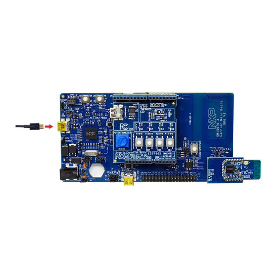
Page 3: Introduction
QN9090 Module board • Generic expansion board Figure 1 Board overview UM11355 All information provided in this document is subject to legal disclaimers. © NXP Semiconductors N.V. 2020. All rights reserved. Rev.1.0 — 15 January 2020 User Guide 3 of 19... -
Page 4: Carrier Main Board
Support for external debug probes. • Power, Reset, ISP and UART Tx/Rx LEDs. UM11355 All information provided in this document is subject to legal disclaimers. © NXP Semiconductors N.V. 2020. All rights reserved. Rev.1.0 — 15 January 2020 User Guide 4 of 19... -
Page 5: Board Layout And Settings
QN9090 Reset LED – LED is on anytime the Target RESET is pulled low. UM11355 All information provided in this document is subject to legal disclaimers. © NXP Semiconductors N.V. 2020. All rights reserved. Rev.1.0 — 15 January 2020 User Guide... - Page 6 Expansion connectors, including Arduino Uno rev3 compatible connectivity. CN3, CN4 JM1, JM2 QN9090 module headers UM11355 All information provided in this document is subject to legal disclaimers. © NXP Semiconductors N.V. 2020. All rights reserved. Rev.1.0 — 15 January 2020 User Guide 6 of 19...
-
Page 7: Led Indicators
QN9090 Reset LED – LED is on anytime the Target RESET is pulled UM11355 All information provided in this document is subject to legal disclaimers. © NXP Semiconductors N.V. 2020. All rights reserved. Rev.1.0 — 15 January 2020 User Guide... -
Page 8: Arduino Connectors
Link2 probe, the USB mini B-type connector (J15) UM11355 All information provided in this document is subject to legal disclaimers. © NXP Semiconductors N.V. 2020. All rights reserved. Rev.1.0 — 15 January 2020 User Guide... -
Page 9: Debug Configurations
To use an external debug probe: • connect the probe to the SWD (P1) connector UM11355 All information provided in this document is subject to legal disclaimers. © NXP Semiconductors N.V. 2020. All rights reserved. Rev.1.0 — 15 January 2020 User Guide 9 of 19... -
Page 10: On-Board Link2 Flash Programing
Fit jumper JP2 across pins 2 - 3 (External Target). UM11355 All information provided in this document is subject to legal disclaimers. © NXP Semiconductors N.V. 2020. All rights reserved. Rev.1.0 — 15 January 2020 User Guide 10 of 19... -
Page 11: Qn9090 Modules
• Infrared Emitting LED Vishay VSMB2948SL connected to QN9090 IO20_IR_Blaster UM11355 All information provided in this document is subject to legal disclaimers. © NXP Semiconductors N.V. 2020. All rights reserved. Rev.1.0 — 15 January 2020 User Guide 11 of 19... -
Page 12: Qn9090 Current Measurement
(IC21) current monitor chip and a 12-bit ADC (ADC122S021, IC19) with a 12-bit sample UM11355 All information provided in this document is subject to legal disclaimers. © NXP Semiconductors N.V. 2020. All rights reserved. Rev.1.0 — 15 January 2020 User Guide... -
Page 13: Vsense Resistor Measurement
This signal goes to the module (JM1.17) and the expansion connector (J3.31) UM11355 All information provided in this document is subject to legal disclaimers. © NXP Semiconductors N.V. 2020. All rights reserved. Rev.1.0 — 15 January 2020 User Guide 13 of 19... - Page 14 To measure the current using multimeter, remove R51 and place the multimeter across J14 pins 1 and 2. Figure 10 R51 Location UM11355 All information provided in this document is subject to legal disclaimers. © NXP Semiconductors N.V. 2020. All rights reserved. Rev.1.0 — 15 January 2020 User Guide 14 of 19...
-
Page 15: Io Considerations
8,9 (UART 0) Remove jumpers on JP4 and JP7 0,1 (UART 1) UM11355 All information provided in this document is subject to legal disclaimers. © NXP Semiconductors N.V. 2020. All rights reserved. Rev.1.0 — 15 January 2020 User Guide 15 of 19... -
Page 16: Running The Dk6 Board At Different Voltages
It is important to leave C49 connected to Pin10 of the FT230A. To achieve this modify the boards as shown in Figure 13. UM11355 All information provided in this document is subject to legal disclaimers. © NXP Semiconductors N.V. 2020. All rights reserved. Rev.1.0 — 15 January 2020 User Guide 16 of 19... - Page 17 NXP Semiconductors QN9090-DK006 Development Kit User Guide Figure 13 3V3OUT modification UM11355 All information provided in this document is subject to legal disclaimers. © NXP Semiconductors N.V. 2020. All rights reserved. Rev.1.0 — 15 January 2020 User Guide 17 of 19...
-
Page 18: Legal Information
For sales office addresses, please send an email to: salesaddresses@nxp.com Date of release: 01/2020 Document identifier: UM11355 UM11355 All information provided in this document is subject to legal disclaimers. © NXP Semiconductors N.V. 2020. All rights reserved. Rev.1.0 — 15 January 2020 User Guide 18 of 19... -
Page 19: Table Of Contents
QN9090 NXP Semiconductors QN9090-DK006 Development Kit User Guide 7. Contents Introduction ............3 Purpose .............. 3 Kit contents ............3 Carrier Main Board ..........4 Feature summary ..........4 Board layout and settings ........5 LED indicators ............ 7 ARDUINO connectors ........8 Buttons ...............
Need help?
Do you have a question about the QN9090-DK006 and is the answer not in the manual?
Questions and answers