
Related Manuals for National Instruments DAQ PCI-4451


Summary of Contents for National Instruments DAQ PCI-4451
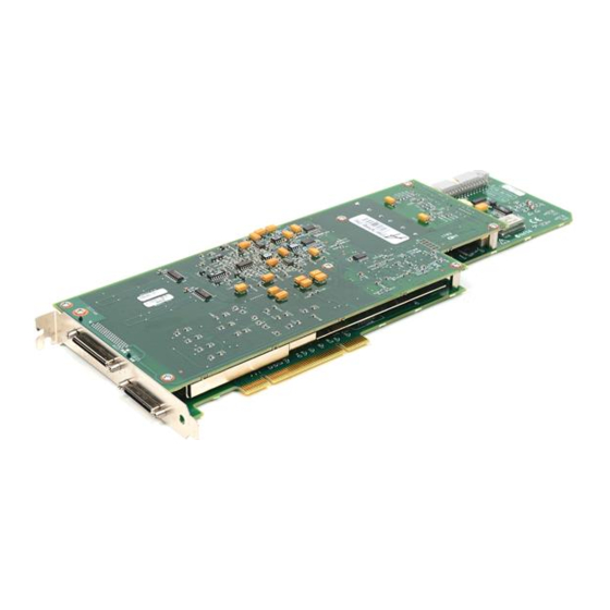
- Page 1 PCI-4451/4452/4453/4454 User Manual Dynamic Signal Acquisition Device for PCI PCI-4451/4452/4453/4454 User Manual March 2000 Edition Part Number 321891B-01...
- Page 2 Sweden 08 587 895 00, Switzerland 056 200 51 51, Taiwan 02 2528 7227, United Kingdom 01635 523545 For further support information, see the Technical Support Resources appendix. To comment on the documentation, send e-mail to techpubs@ni.com © Copyright 1998, 2000 National Instruments Corporation. All rights reserved.
- Page 3 Any action against National Instruments must be brought within one year after the cause of action accrues. National Instruments shall not be liable for any delay in performance due to causes beyond its reasonable control.
-
Page 4: Table Of Contents
Chapter 1 Introduction About the PCI-445X.......................1-1 What You Need to Get Started ..................1-2 Unpacking ........................1-3 Software Programming Choices ..................1-3 National Instruments Application Software ............1-3 NI-DAQ Driver Software ................1-4 Optional Equipment .......................1-5 Custom Cabling ......................1-6 Analog Cables ....................1-6 Analog Accessories ..................1-7 Digital Cables (PCI-4451/4452 Only).............1-7... - Page 5 Contents Digital I/O (PCI-4451/4452 Only) ................3-12 Timing Signal Routing ....................3-13 Programmable Function Inputs (PCI-4451/4452 Only)........3-13 Device and RTSI Clocks................. 3-14 Selecting Sample/Update Clock Frequency ..............3-14 Device Configuration Issues..................3-15 Chapter 4 Signal Connections I/O Connectors....................... 4-1 Analog I/O Connector Signal Descriptions ............
- Page 6 Antialias Filtering....................6-3 The ADC ......................6-9 Noise........................6-10 Analog Output Circuitry (PCI-4451/4453 Only)............6-11 Anti-Image Filtering..................6-12 The DAC ......................6-14 Calibration .......................6-14 Mute Feature....................6-15 Appendix A Specifications Appendix B Pin Connections Appendix C Technical Support Resources Glossary Index © National Instruments Corporation PCI-4451/4452/4453/4454 User Manual...
- Page 7 Contents Figures Figure 1-1. The Relationship between the Programming Environment, NI-DAQ, and Your Hardware............... 1-5 Figure 3-1. Digital Function Block Diagram............3-1 Figure 3-2. PCI-4451/4452 Analog Function Block Diagram ........ 3-2 Figure 3-3. PCI-4453/4454 Analog Function Block Diagram ........ 3-3 Figure 3-4.
- Page 8 Table 4-3. Analog I/O Connector Pin Assignment for the PCI-4453/4454....4-6 Table 4-4. Analog I/O Signal Summary for the PCI-4453/4454......4-7 Table 4-5. Digital I/O Connector Pin Assignment ..........4-9 Table 4-6. Digital I/O Signal Summary..............4-11 © National Instruments Corporation PCI-4451/4452/4453/4454 User Manual...
-
Page 9: About This Manual
Use the manuals you have as follows: • Software documentation—You may have both application software and NI-DAQ software documentation. National Instruments application software includes LabVIEW, LabWindows/CVI, ComponentWorks, Measure, and VirtualBench. After you set up your hardware system, use either your application software documentation or the NI-DAQ documentation to help you write your application. -
Page 10: Related Documentation
The following documents contain information you may find helpful: • BNC-2140 User Manual • BNC-2142 Installation Guide • National Instruments Application Note 025, Field Wiring and Noise Considerations for Analog Signals • PCI Local Bus Specification Revision 2.0 PCI-4451/4452/4453/4454 User Manual www.ni.com... -
Page 11: Introduction
Applications for PCI-445X devices include audio signal processing and analysis, acoustics and speech research, sonar, audio frequency test and measurement, vibration and modal analysis, or any application requiring high-fidelity signal acquisition or generation. © National Instruments Corporation PCI-4451/4452/4453/4454 User Manual... -
Page 12: What You Need To Get Started
Chapter 1 Introduction What You Need to Get Started To set up and use your PCI-445X, you need the following: One of the following PCI-445X devices: – PCI-4451 – PCI-4452 – PCI-4453 – PCI-4454 This manual One or more of the following software packages and documentation: –... -
Page 13: Unpacking
Never touch exposed connector pins. Remove the device from the package and inspect the device for loose components or any other sign of damage. Notify National Instruments if the device appears damaged in any way. Do not install a damaged device into your computer. -
Page 14: Ni-Daq Driver Software
Excel. NI-DAQ Driver Software The NI-DAQ driver software is included with most National Instruments DAQ hardware. NI-DAQ has an extensive library of functions that you can call from your application programming environment. These functions allow you to use all features of your PCI-445X. -
Page 15: Optional Equipment
Figure 1-1. The Relationship between the Programming Environment, NI-DAQ, and Your Hardware Optional Equipment ♦ PCI-4451/4452 National Instruments offers a variety of products to use with your PCI-4451/4452, including these cables and connector blocks: • SHC50-68 digital cable • Shielded and DIN rail-mountable 68-pin connector blocks for digital I/O •... -
Page 16: Custom Cabling
RTSI cable for multiboard synchronization and triggering Custom Cabling National Instruments offers different types of cables in varying lengths, and the BNC-214X DSA accessories to connect your analog I/O to a PCI-445X device. National Instruments also offers cables of different lengths and accessories to connect your digital I/O signals to the PCI-4451/4452. -
Page 17: Analog Accessories
50-position straight cable plug, part number 787131-1 • 50-position backshell with jackscrews, part number 787233-1 Refer to Figure B-2, 68-Pin Digital Connector for Any Digital Accessory, for pin assignments for digital accessories and cables. © National Instruments Corporation PCI-4451/4452/4453/4454 User Manual... -
Page 18: Installation And Configuration
Remove the expansion slot cover on the back panel of the computer. Touch a metal part of the computer chassis with your hand and with the anti-static bag containing your PCI-445X. Remove the PCI-445X from the anti-static bag. © National Instruments Corporation PCI-4451/4452/4453/4454 User Manual... -
Page 19: Device Configuration
Data acquisition related configuration includes such settings as analog input polarity and range, analog input mode, and others. You can modify these settings through National Instruments application level software, such as LabVIEW, LabWindows/CVI, VirtualBench-DSA, and ComponentWorks, or with driver software such as NI-DAQ. -
Page 20: Hardware Overview
General Control FIFO and DMA † AI FIFO AO FIFO Functions Control †† Digital I/O Bus DAQ-STC MITE PCI Controller PCI Bus † PCI-4451/4453 only †† PCI-4451/4452 only Figure 3-1. Digital Function Block Diagram © National Instruments Corporation PCI-4451/4452/4453/4454 User Manual... -
Page 21: Figure 3-2. Pci-4451/4452 Analog Function Block Diagram
Chapter 3 Hardware Overview Figure 3-2. PCI-4451/4452 Analog Function Block Diagram PCI-4451/4452/4453/4454 User Manual www.ni.com... -
Page 22: Figure 3-3. Pci-4453/4454 Analog Function Block Diagram
Chapter 3 Hardware Overview Figure 3-3. PCI-4453/4454 Analog Function Block Diagram © National Instruments Corporation PCI-4451/4452/4453/4454 User Manual... -
Page 23: Analog Input
Chapter 3 Hardware Overview Analog Input The analog input section of each PCI-445X is software configurable. You can select different analog input configurations through application software. The following sections describe in detail each of the analog input categories. Input Mode ♦... -
Page 24: Considerations For Selecting Input Ranges
The input range you select for the PCI-4451/4452 depends on the expected range of the incoming signal. A large input range can accommodate a large signal variation, but reduces the voltage resolution. A smaller input range © National Instruments Corporation PCI-4451/4452/4453/4454 User Manual... -
Page 25: Analog Output (Pci-4451/4453 Only)
Connections that exceed the rated input voltages can damage the computer and Caution the connected equipment. National Instruments is not liable for any damages resulting from such connections. Analog Output (PCI-4451/4453 Only) The analog output section of the PCI-4451/4453 is software-configurable. -
Page 26: Output Polarity And Output Range
The value of 1 LSB of the 16-bit DAC; that is, the voltage increment corresponding to a change of one count in the DAC 16-bit count. See Appendix A, Specifications, for absolute maximum ratings. © National Instruments Corporation PCI-4451/4452/4453/4454 User Manual... -
Page 27: Trigger
Chapter 3 Hardware Overview Note The PCI-4451 boots in a mode with the outputs disabled and infinitely (∞) attenuated. Although these functions appear similar, they are distinct and are implemented to protect your external equipment from startup transients. ♦ PCI-4453 This device does not feature any attenuation setting capability and boots in a mode with outputs disabled. -
Page 28: Figure 3-4. Below-Low-Level Triggering Mode
Figure 3-4. Below-Low-Level Triggering Mode In above-high-level triggering mode, shown in Figure 3-5, the trigger is generated when the signal value is greater than highValue. lowValue is unused. highValue Trigger Figure 3-5. Above-High-Level Triggering Mode © National Instruments Corporation PCI-4451/4452/4453/4454 User Manual... -
Page 29: Figure 3-6. Inside-Region Triggering Mode
Chapter 3 Hardware Overview In inside-region triggering mode, the trigger is generated when the signal value is between lowValue and highValue. highValue lowValue Trigger Figure 3-6. Inside-Region Triggering Mode In high-hysteresis triggering mode, the trigger is generated when the signal value is greater than highValue, with the hysteresis specified by lowValue. - Page 30 PCI-4451/4452/4453/4454 Using digital triggering, you can trigger the PCI-445X from any other National Instruments device that has the RTSI-bus feature and resides on the same PCI bus. You can connect the device through the RTSI bus cable. An external digital trigger can also trigger multiple devices simultaneously by distributing that trigger through the RTSI bus.
-
Page 31: Rtsi Triggers
Chapter 3 Hardware Overview RTSI Triggers The seven RTSI trigger lines on the RTSI bus provide a very flexible interconnection scheme for any PCI-445X device sharing the RTSI bus. These bidirectional lines can drive any of eight timing signals onto the RTSI bus and can receive any of these timing signals. -
Page 32: Timing Signal Routing
I/O connector, software can turn on the output driver for the PFI8/GPCTR0_SOURCE pin. Note Two of the 10 PFI pins are not available for general-purpose input on the digital connector. You can configure PFI2/CONVERT* and PFI5/UPDATE* as outputs only. © National Instruments Corporation 3-13 PCI-4451/4452/4453/4454 User Manual... -
Page 33: Device And Rtsi Clocks
Chapter 3 Hardware Overview Device and RTSI Clocks A PCI-445X can use either its internal 20 MHz timebase or a timebase received over the RTSI bus. In addition, if you configure the device to use the internal timebase, you can program the device to drive its internal timebase over the RTSI bus to another device that you program to receive this timebase signal. -
Page 34: Device Configuration Issues
1.25 kS/s. This minimum rate is required to keep the internal circuitry of the converters running within specifications. You are responsible for selecting sample and update rates that fall within the specified limits. Failure to do so can greatly affect the specifications. © National Instruments Corporation 3-15 PCI-4451/4452/4453/4454 User Manual... -
Page 35: Signal Connections
PCI-445X can damage the device, the computer, and associated accessories. Maximum input ratings for each signal are given in the Protection column of Tables 4-2, 4-4, and 4-6. National Instruments is not liable for any damages resulting from such signal connections. -
Page 36: Analog I/O Connector Signal Descriptions
Chapter 4 Signal Connections Analog I/O Connector Signal Descriptions ♦ PCI-4451/4452 Figure 4-1 shows the analog pin connections for the PCI-4451/4452. –ACH0 +ACH0 † AIGND AIGND –ACH1 +ACH1 † AIGND AIGND –ACH2 +ACH2 † AIGND AIGND –ACH3 +ACH3 † AIGND AIGND †... -
Page 37: Table 4-1. Analog I/O Connector Pin Assignment For The Pci-4451/4452
— — Digital Ground—This pin supplies the reference for the +5 VDC supply. All three ground references—AIGND, AOGND (PCI-4451 only), and DGND—are connected together on your PCI-4451/4452, but each serves a separate purpose. © National Instruments Corporation PCI-4451/4452/4453/4454 User Manual... -
Page 38: Table 4-2. Analog I/O Signal Summary For The Pci-4451/4452
Chapter 4 Signal Connections Table 4-2. Analog I/O Signal Summary for the PCI-4451/4452 Signal Impedance Protection Sink Rise Type and Input/ (Volts) Source (mA at Time Signal Name Direction Output On/Off (mA at V) (ns) Bias † +ACH<0..3> 1 MΩ ±42.4 V/±42.4 V —... -
Page 39: Figure 4-2. Analog Pin Connections For The Pci-4453/4454
+5 V 33 67 +5 V DGND 34 68 DGND PCI-4453 only PCI-4454 only † These CGND pins are not connected in the SHC68-C68-A1 cable. Figure 4-2. Analog Pin Connections for the PCI-4453/4454 © National Instruments Corporation PCI-4451/4452/4453/4454 User Manual... -
Page 40: Table 4-3. Analog I/O Connector Pin Assignment For The Pci-4453/4454
Chapter 4 Signal Connections Table 4-3. Analog I/O Connector Pin Assignment for the PCI-4453/4454 Signal Name Reference Direction Description +ACH<0..3> AIGND Input +Analog Input Channel 0 through 3—The PCI-4453 uses +ACH<0..1> and the PCI-4454 uses +ACH<0..3>. Analog Input Ground (AIGND) is the reference point for single-ended measurements. -
Page 41: Table 4-4. Analog I/O Signal Summary For The Pci-4453/4454
AI = Analog Input AO = Analog Output DIO = Digital Input/Output DO = Digital Output † ±400 V/±400 V guaranteed by design, but not tested or certified to operate beyond ±42.4 V © National Instruments Corporation PCI-4451/4452/4453/4454 User Manual... -
Page 42: Digital I/O Connector Signal Descriptions
Chapter 4 Signal Connections Digital I/O Connector Signal Descriptions ♦ PCI-4451/4452 Figure 4-3 shows the digital pin connections for the PCI-4451/4452. FREQ_OUT DGND PFI9/GPCTR0_GATE GPCTR0_OUT PFI8/GPCTR0_SOURCE DGND UPDATE* PFI6/WFTRIG DGND PFI7 PFI4/GPCTR1_GATE GPCTR1_OUT DGND PFI3/GPCTR1_SOURCE PFI0/TRIG1(EXT_TRIG) PFI1/TRIG2 (PRETRIG) CONVERT* DGND 10 35 DIO7 RESERVED1... -
Page 43: Table 4-5. Digital I/O Connector Pin Assignment
Input PFI3/Counter 1 Source—As an input, this is one of the PFIs. Output As an output, this is the GPCTR1_SOURCE signal. This signal reflects the actual source connected to the general-purpose counter 1. © National Instruments Corporation PCI-4451/4452/4453/4454 User Manual... - Page 44 Chapter 4 Signal Connections Table 4-5. Digital I/O Connector Pin Assignment (Continued) Signal Name Reference Direction Description PFI4/GPCTR1_GATE DGND Input PFI4/Counter 1 Gate—As an input, this is one of the PFIs. Output As an output, this is the GPCTR1_GATE signal. This signal reflects the actual GATE signal connected to the general-purpose counter 1.
-
Page 45: Table 4-6. Digital I/O Signal Summary
DIO = Digital Input/Output DO = Digital Output pu = pullup Note: The tolerance on the 50 kΩ pullup and pulldown resistors is very large. Actual value may range from 17 to 100 kΩ. © National Instruments Corporation 4-11 PCI-4451/4452/4453/4454 User Manual... -
Page 46: Analog Input Signal Connections
Chapter 4 Signal Connections Analog Input Signal Connections ♦ PCI-4451/4452 The analog input signals for the PCI-4451/4452 are +ACH<0..3>, −ACH<0..3>, and AIGND. The +ACH<0..1> signals are tied to the two analog input channels of your PCI-4451; the ±ACH<0..3> are tied to the four analog input channels of your PCI-4452. -
Page 47: Figure 4-5. Analog Input Stage Of The Pci-4453/4454
PCI-4453/4454. Signals are routed to the positive inputs of the analog input stage and their returns to AIGND through a common-mode choke. Your PCI-4453/4454 A/D converters measure these signals when they perform A/D conversions. © National Instruments Corporation 4-13 PCI-4451/4452/4453/4454 User Manual... -
Page 48: Types Of Signal Sources
1 and 100 mV, but can be much higher if power distribution circuits are not properly connected. For this reason, National Instruments does not recommend connecting AIGND or AOGND to the source signal ground system, since the difference between the grounds can induce currents in the PCI-445X ground system. -
Page 49: Figure 4-6. Analog Output Channel Block Diagram For The Pci-4451
AOGND to reduce common-mode noise coupled from an interfering source to the device.You can make DIFF and SE connections through the BNC-2140 accessory. © National Instruments Corporation 4-15 PCI-4451/4452/4453/4454 User Manual... -
Page 50: Analog Power Connections
Do not connect these +5 V power pins directly to analog ground, digital ground, or to any other voltage source on the PCI-445X or any other device. Doing so can damage the PCI-445X device and the computer. National Instruments is not liable for damages resulting from such a connection. -
Page 51: Digital I/O Signal Connections (Pci-4451/4452 Only)
TTL signals and sensing external device states such as the state of the switch shown in Figure 4-8. Digital output applications include sending TTL signals and driving external devices such as the LED shown in Figure 4-8. © National Instruments Corporation 4-17 PCI-4451/4452/4453/4454 User Manual... -
Page 52: Digital Power Connections (Pci-4451/4452 Only)
Chapter 4 Signal Connections Digital Power Connections (PCI-4451/4452 Only) Four pins on the digital I/O connector supply +5 V (+4.65 to +5.25 VDC at 1 A) from the computer power supply through a self-resetting fuse. The fuse resets automatically within a few seconds after an overcurrent condition is removed. -
Page 53: Programmable Function Input Connections (Pci-4451/4452 Only)
Posttriggered data acquisition allows you to view only data that you acquire after receiving a trigger event. A typical posttriggered acquisition sequence is shown in Figure 4-9. TRIG1 CONVERT* Scan Counter Figure 4-9. Typical Posttriggered Acquisition © National Instruments Corporation 4-19 PCI-4451/4452/4453/4454 User Manual... -
Page 54: Pfi0/Trig1 (Ext_Trig) Signal
Chapter 4 Signal Connections Pretriggered data acquisition allows you to view data that you acquire before the trigger of interest in addition to data you acquire after the trigger. Figure 4-10 shows a typical pretriggered acquisition sequence. The description for each signal shown in these figures is included in this chapter. -
Page 55: Pfi1/Trig2 (Pretrig) Signal
In single-pulse mode, software controls the level of the EXTSTROBE* signal. A 10 µs and a 1.2 µs clock is available for generating a sequence © National Instruments Corporation 4-21 PCI-4451/4452/4453/4454 User Manual... -
Page 56: Waveform Generation Timing Connections
Chapter 4 Signal Connections of eight pulses in hardware-strobe mode. Figure 4-11 shows the timing for hardware-strobe mode EXTSTROBE* signal. = 600 ns or 5 µs Figure 4-11. EXTSTROBE* Signal Timing Waveform Generation Timing Connections The waveform generation timing signals are WFTRIG and UPDATE*. WFTRIG Signal Any PFI pin can receive as an input the WFTRIG signal, which is available as an output on the PFI6/WFTRIG pin. -
Page 57: Gpctr0_Source Signal
You can use the GATE signal in a variety of different applications to perform actions such as starting and stopping the counter, generating interrupts, saving the counter contents, and so on. © National Instruments Corporation 4-23 PCI-4451/4452/4453/4454 User Manual... -
Page 58: Gpctr0_Up_Down Signal (Pci-4451/4452 Only)
Chapter 4 Signal Connections As an output, the GPCTR0_GATE signal reflects the actual GATE signal connected to general-purpose counter 0. This is true even if the GATE is externally generated by another PFI signal. This output is set to high-impedance at startup. GPCTR0_OUT Signal This signal is available only as an output on the GPCTR0_OUT pin. -
Page 59: Gpctr1_Gate Signal (Pci-4451/4452 Only)
As an output, the GPCTR1_GATE signal monitors the actual GATE signal connected to general-purpose counter 1. This is true even if the GATE is externally generated by another PFI signal. This output is set to high-impedance at startup. © National Instruments Corporation 4-25 PCI-4451/4452/4453/4454 User Manual... -
Page 60: Gpctr1_Out Signal (Pci-4451/4452 Only)
Chapter 4 Signal Connections GPCTR1_OUT Signal (PCI-4451/4452 Only) This signal is available only as an output on the GPCTR1_OUT pin. The GPCTR1_OUT signal monitors the TC device general-purpose counter 1. You have two software-selectable output options—pulse on TC and toggle output polarity on TC. -
Page 61: Figure 4-16. Gpctr Timing Summary
In this case, GATEs applied close to a SOURCE edge take effect either on that SOURCE edge or on the next one. This arrangement results in an uncertainty of one SOURCE clock period with respect to unsynchronized gating sources. © National Instruments Corporation 4-27 PCI-4451/4452/4453/4454 User Manual... -
Page 62: Freq_Out Signal (Pci-4451/4452 Only)
PCI-445X if you do not take proper care when running signal wires between signal sources and the device. For more information, refer to National Instruments Application Note 025, Field Wiring and Noise Considerations for Analog Signals The following recommendations apply mainly to analog input signal routing to the device, although they also apply to signal routing in general. - Page 63 Minimize cable lengths and use schmitt-trigger devices to deglitch signals. Further conditioning may be required to create a clean signal. • Always try to couple a ground with a signal to minimize noise pickup and radiation. © National Instruments Corporation 4-29 PCI-4451/4452/4453/4454 User Manual...
-
Page 64: Loading Calibration Constants
This chapter discusses the calibration procedures for your PCI-445X. Your PCI-445X comes with a calibration certificate. The certificate contains a unique tracking number linking your device to the National Instruments corporate databases where the traceability information is stored. Calibration refers to the process of minimizing measurement and output voltage errors by making small circuit adjustments. -
Page 65: Self-Calibration
Self-Calibration Your PCI-445X can measure and correct almost all of its calibration-related errors without any external signal connections. Your National Instruments software provides a self-calibration method. This self-calibration process, which generally takes less than a minute, is the preferred method of assuring accuracy in your application. -
Page 66: Traceable Recalibration
If you require factory recalibration, send your PCI-445X back to National Instruments. National Instruments will send the device back to you with a new calibration certificate. Please check with National Instruments for additional information such as cost and delivery times. -
Page 67: Theory Of Analog Operation
–20 to 60 dB in 10 dB increments. The input stage has differential connections, allowing quiet measurement of either single-ended or differential signals. © National Instruments Corporation PCI-4451/4452/4453/4454 User Manual... - Page 68 Chapter 6 Theory of Analog Operation ♦ PCI-4453/4454 The PCI-4453 has two identical analog input channels. The PCI-4454 has four identical analog input channels. An analog input channel is illustrated in Figure 4-5, Analog Input Stage of the PCI-4453/4454. These input channels have 16-bit resolution and are simultaneously sampled at software-programmable rates from 5 to 51.2 kS/s in 47.484 µS/s increments.
-
Page 69: Input Coupling
500 Hz that is input is represented incorrectly as a signal between 0 and 500 Hz. The apparent frequency of this sine wave is the absolute value of the difference between the frequency © National Instruments Corporation PCI-4451/4452/4453/4454 User Manual... - Page 70 Chapter 6 Theory of Analog Operation of the input signal and the closest integer multiple of 1,000 Hz (the sampling rate). Therefore, if a 2,325 Hz sine wave is input, its apparent frequency is: 2,325 − (2)(1,000) = 325 Hz. If a 3,975 Hz sine wave is input, its apparent frequency is: (4)(1,000) −...
-
Page 71: Figure 6-1. Input Frequency Response
Figures 6-1 and 6-2 show the frequency response of the PCI-445X input circuitry. Amplitude (dB) 0.00 –20.00 –40.00 –60.00 –80.00 –100.00 –120.00 0.00 0.20 0.40 0.60 0.80 1.00 Frequency/Sample Rate (f Figure 6-1. Input Frequency Response © National Instruments Corporation PCI-4451/4452/4453/4454 User Manual... -
Page 72: Figure 6-2. Input Frequency Response Near The Cutoff
Chapter 6 Theory of Analog Operation Amplitude (dB) 0.00 –1.00 –2.00 –3.00 –4.00 –5.00 –6.00 0.43 0.44 0.45 0.46 0.47 0.48 0.49 0.50 Frequency/Sample Rate (f Figure 6-2. Input Frequency Response Near the Cutoff Because the ADC samples at 128 times the data rate, frequency components above 64 times the data rate can alias. -
Page 73: Figure 6-3. Alias Rejection At The Oversample Rate For The Pci-4451/4452
5 kS/s 10 kS/s 100 kS/s 1 MS/s Sample Rate 12.8 MHz 128 MHz Over-Sample 128 kHz 1.28 MHz 640 kHz Frequency Figure 6-3. Alias Rejection at the Oversample Rate for the PCI-4451/4452 © National Instruments Corporation PCI-4451/4452/4453/4454 User Manual... -
Page 74: Figure 6-4. Alias Rejection At The Oversample Rate For The Pci-4453/4454
Chapter 6 Theory of Analog Operation Alias Rejection (dB) 0.00 –10.00 –20.00 –30.00 –40.00 –50.00 –60.00 –70.00 –80.00 10 kS/s 1 kS/s 5 kS/s 100 kS/s 1 MS/s Sample Rate 12.8 MHz 128 MHz 128 kHz Over-Sample 640 kHz 1.28 MHz Frequency Figure 6-4. -
Page 75: The Adc
25.6 kHz. This noise is not correlated with the input signal and is almost completely rejected by the digital filter. © National Instruments Corporation PCI-4451/4452/4453/4454 User Manual... -
Page 76: Noise
Chapter 6 Theory of Analog Operation The resulting output of the filter is a band-limited signal with a dynamic range of over 90 dB. One of the advantages of a delta-sigma ADC is that it uses a 1-bit DAC as an internal reference, whereas most 16-bit ADCs use 16-bit resistor-network DACs or capacitor-network DACs. -
Page 77: Analog Output Circuitry (Pci-4451/4453 Only)
±0.2 dB within the frequency range of DC to 23 kHz and has a THD of −90 dB at 1 kHz. With these specifications, you are assured of the quality and integrity of the output signals generated. © National Instruments Corporation 6-11 PCI-4451/4452/4453/4454 User Manual... -
Page 78: Anti-Image Filtering
Chapter 6 Theory of Analog Operation Anti-Image Filtering A sampled signal repeats itself throughout the frequency spectrum. These repetitions begin above one-half the sample rate (F s ) and, theoretically, continue up through the spectrum to infinity, as shown in Figure 6-6a. Because the sample data actually represents only the frequency components below one-half the sample rate (the baseband), it is desirable to filter out all these extra images of the signal. -
Page 79: Figure 6-6. Signal Spectra In The Dac
Images After the DAC Baseband Signal 16 F Frequency c. Spectrum of Signal After DAC Baseband Signal 16 F Frequency d. Spectrum of Signal After Analog Filters Figure 6-6. Signal Spectra in the DAC © National Instruments Corporation 6-13 PCI-4451/4452/4453/4454 User Manual... -
Page 80: The Dac
Chapter 6 Theory of Analog Operation The DAC The 64-times oversampling delta-sigma DACs on the PCI-4451/4453 work in the same way as delta-sigma ADCs, only in reverse. The digital data first passes through a digital lowpass filter and then goes to the delta-sigma modulator. -
Page 81: Mute Feature
DAC has one offset for the first 4,096 zero samples and another offset in mute mode for as long as zeros are sent. This difference is usually less than 1 mV. © National Instruments Corporation 6-15 PCI-4451/4452/4453/4454 User Manual... -
Page 82: Appendix A Specifications
Type of ADC.......... Delta-sigma, 128-times oversampling Sample rates Device Sample Rates 4451 5 kS/s to 204.8 kS/s in increments of 190.735 µS/s 4452 4453 5 kS/s to 51.2 kS/s in increments of 47.684 µS/s 4454 © National Instruments Corporation PCI-4451/4452/4453/4454 User Manual... - Page 83 Appendix A Specifications Frequency accuracy ........±25 ppm Input signal ranges (software selectable for PCI-4451/4452) Gain Device Linear Full-scale Range (Peak) −20 dB 4451/4452 ±42.4 V −10 dB 0.316 ±31.6 V 0 dB ±10.0 3.16 +10 dB ±3.16 V +20 dB ±1.00 V 31.6 +30 dB...
- Page 84 0 dB ±0.1 dB, 0 to 23 kHz, 51.2 kS/s, DC coupling −3 dB bandwidth ........0.493 f Input coupling ........AC or DC, software-selectable AC −3 dB cutoff frequency .... 3.4 Hz © National Instruments Corporation PCI-4451/4452/4453/4454 User Manual...
- Page 85 Appendix A Specifications Common-mode range Device Gain Common Mode Range Gain ≥ 0 dB both + and − should remain within ±12 V 4451/4452 of AIGND both + and − should remain within ±42.4 V Gain < 0 dB of AIGND 4453/4454 Gain = 0 dB + should remain within...
-
Page 86: Figure A-1. Pci-4451/4452 Idle Channel Noise (Typical
Alias rejection ........80 dB, 0.536 f < f < 63.464 f Spurious-free dynamic range ....95 dB THD ............−80 dB; −90 dB for f < 20 kHz or signal < 1 V © National Instruments Corporation PCI-4451/4452/4453/4454 User Manual... - Page 87 Appendix A Specifications IMD ............−100 dB (CCIF 14 kHz + 15 kHz) Crosstalk (channel separation)....−100 dB, DC to 100 kHz Phase linearity Device Gain Phase Linearity ≥ 0 dB 4451/4452 ±1° < 0 dB ±2° 4453/4454 0 dB ±1° Interchannel phase Device Gain Interchannel Phase...
- Page 88 FIFO buffer size ........512 samples Data transfers ......... DMA, programmed I/O, Interrupt Transfer Characteristics Offset (residual DC)....... ±5 mV max, any gain Gain (amplitude accuracy) ..... ±0.1 dB, f = 1 kHz © National Instruments Corporation PCI-4451/4452/4453/4454 User Manual...
- Page 89 Appendix A Specifications Voltage Output Characteristics Output impedance PCI-4451..........22 Ω between +DACxOUT and −DACxOUT, 4.55 kΩ to AOGND PCI-4453..........22 Ω between +DACxOUT and AO_SHLD Flatness (relative to 1 kHz).....±0.2 dB, 0 to 23 kHz, 51.2 kS/s −3 dB bandwidth........0.492 f Output coupling ........DC Short-circuit protection PCI-4451..........yes (+ and −...
- Page 90 4.35 V — Power-on state........Input (high-impedance) Data transfers ......... Programmed I/O Timing I/O Number of channels ....... 2 up/down counter/timers, 1 frequency scaler Resolution Counter/timers ........ 24 bits Frequency scaler ......4 bits © National Instruments Corporation PCI-4451/4452/4453/4454 User Manual...
- Page 91 Appendix A Specifications Compatibility ..........TTL/CMOS Base clocks available Counter/timers .........20 MHz, 100 kHz Frequency scaler......10 MHz, 100 kHz Base clock accuracy........±0.01% Max source frequency......20 MHz Min source pulse duration .....10 ns, edge-detect mode Min gate pulse duration ......10 ns, edge-detect mode Data transfers ..........DMA, interrupts, programmed I/O DMA modes ...........Scatter gather...
- Page 92 Requirements ........+5 V, 850 mA idle, 1.0 A active +12 V, 100 mA typical (not including momentary relay switching) −12 V, 40 mA typical +3.3 V, unused Available power Analog I/O connector) ..... +4.65 to +5.25 VDC at 1.0 A © National Instruments Corporation A-11 PCI-4451/4452/4453/4454 User Manual...
- Page 93 Appendix A Specifications PCI-4454 Requirements........+5 V, 1.35 A idle, 1.5 A active +12 V, 150 mA typical (not including momentary relay switching) −12 V, unused +3.3 V, unused Available power Analog I/O connector)....+4.65 to +5.25 VDC at 1.0 A Physical Dimensions (not including connectors) ......10.65 by 31.19 by 1.84 cm (4.19 by 12.28 by 0.73 in.)
-
Page 94: Figure B-1. Db-25 Pinout For The Shc68-Db25 Cable
68-pin digital accessories for the PCI-4451 and PCI-4452 devices. +ACH0 –ACH0 +ACH1 –ACH1 +ACH2 –ACH2 +ACH3 –ACH3 +DAC0OUT –DAC0OUT +DAC1OUT –DAC1OUT +5 V Figure B-1. DB-25 Pinout for the SHC68-DB25 Cable © National Instruments Corporation PCI-4451/4452/4453/4454 User Manual... -
Page 95: Appendix B Pin Connections
Appendix B Pin Connections FREQ_OUT DGND PFI9/GPCTR0_GATE DGND GPCTR0_OUT DGND PFI8/GPCTR0_SOURCE DGND UPDATE* DGND PFI6/WFTRIG DGND PFI7 DGND PFI4/GPCTR1_GATE DGND GPCTR1_OUT DGND PFI3/GPCTR1_SOURCE 10 44 DGND PFI0/TRIG1 (EXT_TRIG) DGND 11 45 PFI1/TRIG2 (PRETRIG) DGND 12 46 13 47 DGND CONVERT* DGND 14 48 RESERVED1... - Page 96 Technical Support Resources This appendix describes the comprehensive resources available to you in the Technical Support section of the National Instruments Web site and provides technical support telephone numbers for you to use if you have trouble connecting to our Web site or if you do not have internet access.
- Page 97 If you have trouble connecting to our Web site, please contact your local National Instruments office or the source from which you purchased your National Instruments product(s) to obtain support. For telephone support in the United States, dial 512 795 8248. For...
- Page 98 Numbers/Symbols ° degree Ω percent positive of, or plus – negative of, or minus amperes alternating current AC coupled allowing the transmission of AC signals while blocking DC signals analog-to-digital © National Instruments Corporation PCI-4451/4452/4453/4454 User Manual...
- Page 99 Glossary analog-to-digital converter—an electronic device, often an integrated circuit, that converts an analog voltage to a digital number ADC resolution the size of the discrete steps in the ADCs input-to-output transfer function; therefore, the smallest voltage difference an ADC can discriminate with a single measurement AI Convert LabVIEW name for CONVERT*.
- Page 100 Also called software triggering. © National Instruments Corporation PCI-4451/4452/4453/4454 User Manual...
- Page 101 Glossary conversion device device that transforms a signal from one form to another. For example, analog-to-digital converters (ADCs) for analog input, digital-to-analog converters (DACs) for analog output, digital input or output ports, and counter/timers are conversion devices. conversion time the time required, in an analog input or output system, from the moment a channel is interrogated (such as with a read instruction) to the moment that accurate data is available CONVERT*...
- Page 102 See port. digital trigger a TTL level signal having two discrete levels—a high and a low level © National Instruments Corporation PCI-4451/4452/4453/4454 User Manual...
- Page 103 Glossary digital input/output direct memory access—a method by which data can be transferred to/from computer memory from/to a device or memory on the bus while the processor does something else. DMA is the fastest method of transferring data to/from computer memory. differential nonlinearity—a measure in LSBs of the worst-case deviation of code widths from their ideal value of 1 LSB down counter...
- Page 104 GPCTR0_GATE general-purpose counter timer 0 gate signal GPCTR0_OUT general-purpose counter timer 0 output signal © National Instruments Corporation PCI-4451/4452/4453/4454 User Manual...
- Page 105 Glossary GPCTR0_SOURCE general-purpose counter timer 0 clock source signal GPCTR1_GATE general-purpose counter timer 1 gate signal GPCTR1_OUT general-purpose counter timer 1 output signal GPCTR1_SOURCE general-purpose counter timer 1 clock source signal grounded measurement See SE. system hour hardware the physical components of a computer system, such as the circuit boards, plug-in boards, chassis, enclosures, peripherals, and cables hardware triggering a form of triggering where you set the start time of an acquisition and gather...
- Page 106 DAQ device are not affected by differences in ground potentials. kilo—the standard metric prefix for 1,000, or 10 , used with units of measure such as volts, hertz, and meters 1,000 samples © National Instruments Corporation PCI-4451/4452/4453/4454 User Manual...
- Page 107 NI-DAQ National Instruments driver software for DAQ hardware noise an undesirable electrical signal—Noise comes from external sources such as the AC power line, motors, generators, transformers, fluorescent lights, soldering irons, CRT displays, computers, electrical storms, welders, radio transmitters, and internal sources such as semiconductors, resistors, and capacitors.
- Page 108 Nyquist frequency © National Instruments Corporation G-11 PCI-4451/4452/4453/4454 User Manual...
- Page 109 Glossary passband the range of frequencies which a device can properly propagate or measure Peripheral Component Interconnect—a high-performance expansion bus architecture originally developed by Intel to replace ISA and EISA. It is achieving widespread acceptance as a standard for PCs and work-stations; it offers a theoretical maximum transfer rate of 132 Mbytes/s.
- Page 110 See SE. RTSI bus real-time system integration bus—the National Instruments timing bus that connects DAQ devices directly, by means of connectors on top of the boards, for precise synchronization of functions seconds...
- Page 111 Glossary a type of coaxial connector signal-to-noise ratio—the ratio of the overall rms signal level to the rms noise level, expressed in decibels software trigger a programmed event that triggers an event such as data acquisition software triggering a method of triggering in which you simulate an analog trigger using software.
- Page 112 UPDATE* update signal update rate the number of output updates per second volts collector common voltage—power supply voltage volts in © National Instruments Corporation G-15 PCI-4451/4452/4453/4454 User Manual...
- Page 113 Glossary reference voltage volts direct current virtual instrument—(1) a combination of hardware and/or software elements, typically used with a PC, that has the functionality of a classic stand-alone instrument; (2) a LabVIEW software module (VI), which consists of a front panel user interface and a block diagram program waveform multiple voltage readings taken at a specific sampling rate WFTRIG...
- Page 114 4-19 to 4-22 ADC, 6-9 to 6-10 CONVERT* signal, 4-21 antialias filtering, 6-3 to 6-9 EXTSTROBE* signal, 4-21 to 4-22 calibration, 6-3 PFI0/TRIG1 (EXT_TRIG) signal, 4-20 input coupling, 6-3 PFI1/TRIG2 (PRETRIG) signal, 4-21 noise, 6-10 © National Instruments Corporation PCI-4451/4452/4453/4454 User Manual...
- Page 115 Index analog I/O connector signal descriptions analog trigger, 3-8 to 3-12 pin assignments (table) above-high-level analog triggering mode (figure), 3-9 PCI-4451/4452, 4-3 below-low-level analog triggering mode PCI-4453/4454, 4-6 (figure), 3-9 pin connections (figure) high-hysteresis analog triggering mode PCI-4451/4452, 4-2 (figure), 3-10 PCI-4453/4454, 4-5 inside-region analog triggering mode signal summary (table)
- Page 116 I/O signal summary (table), 4-4 digital I/O pin assignments (table), 4-9 analog output signal connections, digital I/O signal summary (table), 4-11 4-14 to 4-15 timing connections, 4-21 data acquisition timing connections. See acquisition timing connections. © National Instruments Corporation PCI-4451/4452/4453/4454 User Manual...
- Page 117 Index DC input coupling, 3-4 DIO<0..7> signal DDS (direct digital synthesis) digital I/O pin assignments (table), 4-9 technology, 3-14 digital I/O signal connections, 4-17 delta-sigma converters digital I/O signal summary (table), 4-11 configuration issues, 3-15 direct digital synthesis (DDS) triggering effect, 3-8 technology, 3-14 delta-sigma modulation documentation...
- Page 118 3-6 to 3-8 digital I/O, 4-11 analog trigger, 3-8 to 3-12 block diagrams analog function, 3-2 to 3-3 digital function, 3-1 jitter, with triggering, 3-8 to 3-9 digital I/O, 3-12 to 3-13 © National Instruments Corporation PCI-4451/4452/4453/4454 User Manual...
- Page 119 PFI1/TRIG2 (PRETRIG) signal digital I/O pin assignments (table), 4-9 digital I/O signal summary (table), 4-11 timing connections, 4-21 National Instruments Web support, C-1 to C-2 PFI3/GPCTR1_SOURCE signal NI-DAQ driver software, 1-4 to 1-5 digital I/O pin assignments (table), 4-9 noise, avoiding, 4-28 to 4-29, 6-10...
- Page 120 RTSI bus signal connection (figure), 3-12 connections, 4-19 RTSI clocks, 3-14 waveform generation timing RTSI trigger lines connections, 4-22 overview, 3-12 types of signal sources, 4-14 signal connection (figure), 3-12 floating, 4-14 ground-referenced, 4-14 © National Instruments Corporation PCI-4451/4452/4453/4454 User Manual...
- Page 121 LabVIEW and LabWindows/CVI application software, 1-3 to 1-4 EXTSTROBE* signal, 4-21 to 4-22 Measure, 1-4 PFI0/TRIG1 (EXT_TRIG) signal, 4-20 National Instruments application software, 1-3 to 1-4 PFI1/TRIG2 (PRETRIG) signal, 4-21 NI-DAQ driver software, 1-4 to 1-5 typical posttriggered acquisition VirtualBench, 1-4...
- Page 122 4-22 mode, 3-10 UPDATE* signal, 4-22 inside-region triggering mode WFTRIG signal, 4-22 (figure), 3-10 Web support from National Instruments, low-hysteresis triggering mode, 3-10 C-1 to C-2 specifications, A-10 online problem-solving and diagnostic digital, specifications, A-10 resources, C-1...
Need help?
Do you have a question about the DAQ PCI-4451 and is the answer not in the manual?
Questions and answers