Pioneer RMX-1000 Service Manual
Hide thumbs
Also See for RMX-1000:
- Operating instructions manual (76 pages) ,
- Important notice (4 pages) ,
- Operating instructions manual (28 pages)
Table of Contents
Advertisement
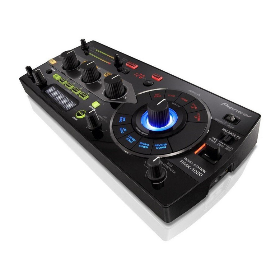
REMIX STATION
RMX-1000
THIS MANUAL IS APPLICABLE TO THE FOLLOWING MODEL(S) AND TYPE(S).
Model
Type
RMX-1000
UXJCB
RMX-1000
SVWYXJ5
RMX-1000
FWLWPWXJ
RMX-1000
KXJ5
RMX-1000
AXJ5
PIONEER CORPORATION
PIONEER ELECTRONICS (USA) INC. P.O. Box 1760, Long Beach, CA 90801-1760, U.S.A.
PIONEER EUROPE NV Haven 1087, Keetberglaan 1, 9120 Melsele, Belgium
PIONEER ELECTRONICS ASIACENTRE PTE. LTD. 253 Alexandra Road, #04-01, Singapore 159936
PIONEER CORPORATION
Power Requirement
AC 100 V to 240 V
AC 100 V to 240 V
AC 100 V to 240 V
AC 100 V to 240 V
AC 100 V to 240 V
1-1, Shin-ogura, Saiwai-ku, Kawasaki-shi, Kanagawa 212-0031, Japan
2012
RMX-1000
K-MZV APR.
ORDER NO.
RRV4310
Remarks
2012 Printed in Japan
Advertisement
Table of Contents

Related Manuals for Pioneer RMX-1000


Summary of Contents for Pioneer RMX-1000
- Page 1 PIONEER CORPORATION 1-1, Shin-ogura, Saiwai-ku, Kawasaki-shi, Kanagawa 212-0031, Japan PIONEER ELECTRONICS (USA) INC. P.O. Box 1760, Long Beach, CA 90801-1760, U.S.A. PIONEER EUROPE NV Haven 1087, Keetberglaan 1, 9120 Melsele, Belgium PIONEER ELECTRONICS ASIACENTRE PTE. LTD. 253 Alexandra Road, #04-01, Singapore 159936...
-
Page 2: Safety Information
PIONEER Service Manual. A subscription to, or additional copies of, Also test with plug reversed Earth PIONEER Service Manual may be obtained at a nominal (Using AC adapter ground charge from PIONEER. plug as required) -
Page 3: Table Of Contents
10.15 VOLTAGES ................................100 10.16 WAVEFORMS................................. 104 11. PCB CONNECTION DIAGRAM ............................110 11.1 MAIN, CDCB and TRIM ASSYS..........................110 11.2 PNCE ASSY ................................114 11.3 PNLE, PARAM, SPFX, SSWB and 7SEG ASSYS ....................118 12. PCB PARTS LIST ................................122 RMX-1000... -
Page 4: Service Precautions
• If calibration data in the software are damaged • If the K0R UCOM, which performs AD conversion of positioning data (voltage value) of the RELEASE FX lever, is replaced For details, see "8.1 NECESSARY ITEMS TO BE NOTED." RMX-1000... -
Page 5: Specifications
Phone jack (Ø 6.3 mm)............1 set OUTPUT terminals RCA pin jacks ..............1 set Phone jack (Ø 6.3 mm)............1 set USB terminal B type .................. 1 set — The specifications and design of this product are subject to change without notice. RMX-1000... -
Page 6: Basic Items For Service
For firmware update, only SD memory cards or SDHC memory cards conforming to SD standards can be used. remixbox Supplied software Read / Write user data, please download remix box from the pioneer homepage. Lubricants and Glues List Name Part No. Remarks... -
Page 7: Pcb Locations
Description Part No. LIST OF ASSEMBLIES 1..MOTHER ASSY DWM2453 1..PANEL ASSY DWM2454 2..MAIN ASSY DWX3315 2..PNCE ASSY DWX3317 2..CDCB ASSY DWX3316 2..PNLE ASSY DWX3318 2..TRIM ASSY DWX3319 2..SSWB ASSY DWX3320 2..SPFX ASSY DWX3321 2..PARAM ASSY DWX3322 2..7SEG ASSY DWX3323 RMX-1000... -
Page 8: Block Diagram
The > mark found on some component parts indicates the importance of the safety factor of the part. Therefore, when replacing, be sure to use parts of identical designation. : The power supply is shown with the marked box. RMX-1000... - Page 9 C N 7 0 0 4 V K N 1 2 9 9 - A D K N 1 6 4 7 - A L=85mm,P=1.0mm H=6mm,Same side LED_GRID6A 7P FFC LED_GRID5A XLED_SEG4 DDD1596 XLED_SEG3 V+3R3REF L=120mm,P=1.0mm VR_RELEASE_FX H=6mm,Reverse GNDREF RMX-1000...
-
Page 10: Audio System Block Diagram
SW (CONN ECTION) 16 bit 16 bit 16 bit UHPI IC 2503 G_SEL INPUT SDRAM IC 3502 IC 4007 D810 +4dB/ McASP1 - 10dB PC M1804 EMIFB PHONE 32 bit 16 bit TRIM ASSY IC 3501 INPUT VR SDRAM RMX-1000... - Page 11 IC 6001 RSPI1 C DC CINx X 5 CDCB ASSY G_SEL G_SEL O UT PUT IC 3502 IC 5001 D810 +4dB/ McASP1 - 10dB AK4382 EMIFB PHONE 32 bit 16 bit AC ADAPT E R (DWR1525) IC 3503 SDRAM RMX-1000...
-
Page 12: Dsp Block Diagram
4.3 DSP BLOCK DIAGRAM MASTER/ Mute control SEND RETURN of Gain switch SELECT INPUT X-PAD FX INPUT X-PAD LEVEL INPUT LEVEL Input Mute PHONE Source Select Roll X- PAD PITCH Oscillator SD Source X-PAD Detect Input sound level Detect RMX-1000... - Page 13 Output OUTPUT LEVEL ISOLATE SCENE RELEASE PHONO Input sound level Detect RMX-1000...
-
Page 14: Power Block Diagram
4.4 POWER BLOCK DIAGRAM DCDC S1001 POWER SW AC Adapter V+4R7E (DC5V/2A) V+5ADP V+18A Q1014 IC1005 FET SW BD9851EFV V-18A IC1003 V+6V BD8152FVM IC1004 V+1R2D R1232D001C IC1002 V+3R3D S-1170B33UC-OTS RMX-1000... - Page 15 IC1006 V+5A NJM2888F05 PCM1804DB IC5001 AK4382AVT OP-AMP NJM4565MD IC4007 IC1007 V+3R3A PCM1804DB NJM2878F3-33 IC3502 V+1R2D D810K013BZKB400 IC2502 SH UCOM R5S72624P144FP IC3502 V+3R3D D810K013BZKB400 IC2502 SH UCOM R5S72624P144FP IC3501, IC3503 SDRAM(256M) IC2503 SDRAM(64M) IC2501 SERIAL FLASH(16M) IC6001 AD7147ACPZ500RL7 SD CARD RMX-1000...
-
Page 16: Clock Map Diagram
DA TA D810K013BZKB400 MC LK(24.576MHz) IC5001 B IC K(3.072MHz) LRC K(48kHz) AK4382AVT SDTI A DD IC2503 SDRAM1 M12L64164A (64M CL=2) 24.576MHz C C LK(1MHz) C DTI SC K(1.667MHz) SI/ SO CN2504 PNCE ASSY CN7001 IC7002 K0R UCOM DYW1811 20MHz RMX-1000... - Page 17 For lines in which multiple lines are integrated such as a data bus, CN6001 the resistance constant for each line may be different from that indicated in the figure above. (For precise values, see the circuit diagrams.) IC6001 AD7147 CDCB ASSY RMX-1000...
-
Page 18: Power Reset Mute Map Diagram
At Power OFF At Power OFF (Power SW) (AC power cord discconected) AC adapter Power SW Power SW AC adapter AC power cord connected disconnected disconnected V+ADP5 STBY Power V+4R7E,V+3R3E K0R_reset FET_SW_CTRL MAIN Power CPU_MUTE MUTE V+3R3D V+1R2D SH_reset DSP_reset AD/DA_reset RMX-1000... - Page 19 LMUTE V+3R3E CMUTE V+3R3E DC JACK Power SW V- 15A (JA1001) (S1001) CPU_MUTE Reset FET_SW_ADP FET SW V+5ADP (Q1014) MAIN Power Note: Power line Reset line Control signal line Clock line The dotted line parts are standby circuits. (no-mount) RMX-1000...
-
Page 20: Power Gnd Map Diagram
±18 V-15A NJM79L15UA IC4007 GNDA NJM2878F3-33 NJM288 V+3R3A V+5A IC1007 3R3A IC5001 GNDA CDCB ASSY IC6001 PNCE ASSY GNDF (Electrostatic path pattern) Metal Plate Spring Ring Scan shield CN7002 Connector CN7301 Connector Screw X-PAD LV PNLE ASSY GND line RMX-1000... - Page 21 Metal SD terminal plate V+1R2D IC1004 1R2D CN2504 Connector CN7001 Connector V+3R3REF IC7002 UCOM Spring Ring CN7004 CN7003 JH7001 Connector Connector Connector PARAM ASSY SPFX ASSY CN7801 CN7701 CN7501 Connector Connector Connector 7SEG ASSY SSWB ASSY PARAM RELESE_FX Screw RMX-1000...
-
Page 22: Matrix Table
SPI RAL DOW N SETTI NG : Slide SW KEY_SEG5 OVERDUB HOLD RELEASE FX (2 position) No marks : Tact SW (3 position) KEY_SEG6 I NPUT X- PAD REVERB UP KEY_SEG7 BANK Note: TAP and NUDGE+/NUDGE- are directly controlled by SH UCOM. RMX-1000... - Page 23 RMX-1000...
-
Page 24: Diagnosis
ADC reset Reset 100 msec wait Reset DAC reset 5+α usec required for the signal to become high from low Canceling of ADC reset (2nd time) Startup (2nd time) Canceling of DAC reset (2nd time) Startup (2nd time) RMX-1000... - Page 25 Continuation of SH communication (normal) CPU_MUTE OFF between DSP and HPI (normal) 3200 ms Initialization of the Cente memory pool Initialization of the Cente USB module Creation of subtask and startup 3300 ms Normal state after normal startup K0R UCOM SH UCOM RMX-1000...
-
Page 26: Troubleshooting
Item to be Checked Corrective Action Reference Defective Test mode Check that buttons, SWs, VRs works Each parts may be defective. Replace it. 6.1 TEST MODE button/SW/VR correctly in the test mode. Terminal of IC7002 may be defective. Replace it. RMX-1000... - Page 27 Replace it. analog circuit 8-4 Defective MUTE circuit Check for the correct waveforms output Q5001, Q5002, Q5003, Q5014, Q7002 may 10.16 WAVEFORMS MUTE circuit waveform from each points. be defective. Replace it. 74 75 76 98 RMX-1000...
- Page 28 RemixBox. 12-2 Defective MAIN Assy: Check for the correct waveforms output IC2501 or IC2502 may be defective. 10.16 WAVEFORMS SH UCOM, FLASH_CLK, from each points. Replace it. 18 19 FLASH Memory FLASH_SI RMX-1000...
-
Page 29: Voltage Monitoring Circuit
FET SW OFF Abnormal: Low level (0 V) -> Power supply stop FET_SW_ADP FET SW Always power supply (Power SW: ON) IC7002 3.3V K0R UCOM Reg IC STB_LED_SEL Power SW adapter CARD (DC 5 V) SD-LED Flashing when an error occurs RMX-1000... - Page 30 Detection of excess voltage voltage decrease V+15A 11.3 V or less V-15A -9.28 V or less V+5A 6.35 V or higher V+6D 8.51 V or higher 4.29 V or less V+3R3D 4.38 V or higher 2.15 V or less RMX-1000...
-
Page 31: Error Indications
SD card. When a USB device is connected, the PC is attempting to mount an SD card or mounting of an SD card has been completed. Normal status This unit has completed mounting of an SD card. RMX-1000... -
Page 32: Usb Diagnosis Method
5.5 USB DIAGNOSIS METHOD Preinclination Provide remixbox installed PC and USB cable. RemixBox, the software supplied to the RMX-1000, enables customization of effects parameters and import of sampling sound sources. RemixBox can be used with the following operating systems: Procedure 1 Turn on the PC, and start up remixbox. -
Page 33: Ic Information
5.6 IC INFORMATION R5S72624P144FP (MAIN ASSY: IC2502) SH UCOM • Pin Function Name for RMX-1000 Function PC2/RD/xWR Connect to SDRAM PC3/xWE0/DQML DQML Connect to SDRAM PC4/xWE1/DQMU/xWE xWE1/DQMU Connect to SDRAM/DSP (HDS2) PC5/xRAS/TIOC4A /IRQ4 xRAS Connect to SDRAM PC6 / xCAS/TIOC4B/IRQ5... - Page 34 • Pin Function Name for RMX-1000 Function PA1/MD_BOOT0 PA1/MD_BOOT0 MD_BOOT0 = 1 PA0/MD_BOOT1 PA0/MD_BOOT1 MD_BOOT0 = 0 GND pin PVcc PVcc Power supply pin (for IO +3.3 V) RTC_X1 NC (RTC_X1) Not used (GND) RTC_X2 NC (RTC_X2) Not used (OPEN)
- Page 35 • Pin Function Name for RMX-1000 Function 101 PG17/LCD_HSYNC/TIOC1B/RSPCK1/RxD6 RSPCK1 (CDC_SCK) Connect to CDC 102 PG16/LCD_VSYNC/TIOC1A/TxD3/ xCTS1 PG16 (GAIN_SW) GAIN_SW 103 PG15/LCD_DATA15/TIOC0D/RxD3/xRTS1 PG15 (BYPASS) BYPASS switch 104 PG14/LCD_DATA14/TIOC0C/SCK1 SCK1 (DAC_SCK) DAC control 105 PG13/LCD_DATA13/TIOC0B/TxD1 TxD1 (DAC_SO) DAC control 106 PVcc PVcc Power supply pin (for IO +3.3 V)
- Page 36 • Pin Function Name for RMX-1000 Function 151 PE0/SCL0/AUDIO_CLK/IRQ0 IRQ0 (HPI_xINIT) I(s) Connect to DSP (xHINT) 152 PVcc PVcc Power supply pin (for IO +3.3V) 153 Vss GND pin 154 PD15/D15/NAF7/PWM2H Connect to SDRAM/DSP 155 PD14/D14/NAF6/PWM2G Connect to SDRAM/DSP 156 PD13/D13/NAF5/PWM2F...
- Page 37 D810K013BZKB400 (MAIN ASSY: IC3502) • Pin Function Name for RMX-1000 Function VSS(Ground) GND pin VSS(Ground) GND pin VSS(Ground) GND pin AHCLKR0/GP2[14]/BOOT[11] NC (GP2[14]) DSP_CTRL standby AXR0[11]/AXR2[0]/GP3[11] GP3[11] Debugging land AXR0[7]/GP3[7] GP3[7] Debugging land AXR0[3]/AXR2[2]/GP3[3] GP3[3] RESET_AD_DA xEMB_RAS xEMB_RAS Connect to SDRAM...
- Page 38 • Pin Function Name for RMX-1000 Function PLL0_VDDA PLL0_VDDA Analog power supply for PLL (1.2 V) USB0_ID NC (USB0_ID) Not used (OPEN) USB0_VBUS NC (USB0_VBUS) Not used (OPEN) AMUTE1/EHRPWMTZ/GP4[14] NC (GP4[14]) Not used (OPEN) AFSX0/GP2[13]/BOOT[10] NC (GP2[13]) Not used (OPEN)
- Page 39 • Pin Function Name for RMX-1000 Function RTC_CVDD RTC_CVDD Not used (Connect to power) RTC_VSS RTC_VSS Not used (Connect to GND) xRESET RESET Reset pin USB0_DM NC (USB0_DM) Not used (OPEN) DVDD(I/Osupply) DVDD Power supply pin (for IO +3.3 V)
- Page 40 • Pin Function Name for RMX-1000 Function CVDD(Coresupply) CVDD Powe supply pin (for core +1.2 V) CVDD(Coresupply) CVDD Powe supply pin (for core +1.2 V) VSS(Ground) GND pin VSS(Ground) GND pin K10 CVDD(Coresupply) CVDD Powe supply pin (for core +1.2 V)
- Page 41 • Pin Function Name for RMX-1000 Function N11 EMA_A[12]/GP1[12] NC (GP1[12]) Not used (OPEN) N12 EMA_D[8]/UHPI_HD[8]/GP0[8] UHPI_HD[8] Connect to HPI N13 EMA_D[6]/MMCSD_DAT[6]/UHPI_HD[6]/GP0[6] UHPI_HD[6] Connect to HPI N14 EMA_D[14]/UHPI_HD[14]/GP0[14] UHPI_HD[14] Connect to HPI N15 EMA_D[5]/MMCSD_DAT[5]/UHPI_HD[5]/GP0[5] UHPI_HD[5] Connect to HPI N16 EMA_D[13]/UHPI_HD[13]/GP0[13]...
- Page 42 DYW1811 (PNCE ASSY: IC7002) K0R UCOM • Pin Function Name for RMX-1000 Function P60/SCL0 LED_GRID0 LED matrix grid selection signal 0 P61/SDA0 LED_GRID1 LED matrix grid selection signal 1 LED_GRID2 LED matrix grid selection signal 2 LED_GRID3 LED matrix grid selection signal 3...
- Page 43 • Pin Function Name for RMX-1000 Function AVSS GND (AD/DA) P157/ANI15 VR_PARAM1 [AD] "SUB PARAMETER1" VR voltage P156/ANI14 VR_HI [AD] "HI" VR voltage P155/ANI13 VR_LEVEL [AD] "LEVEL" VR voltage P154/ANI12 VR_PITCH [AD] "PITCH" VR voltage P153/ANI11 VR_LOW [AD] "LOW" VR voltage...
-
Page 44: Service Mode
X-PAD button ROLL button ON STANDBY button switch Mode 4 Test Mode Mode 11 (Mode 1) Mode 5 Mode 10 Mode 6 Mode 9 Mode 8 Mode 7 Test Mode : CANCEL (Rear panel) ON STANDBY switch POWER SW RMX-1000... - Page 45 ISOLATE FX LOW or MID control. Control LED to be lit Remarks ISOLATE FX LOW knob SCENE FX indicator (red) "MIN": To be unlit "MAX": Maximum luminance ISOLATE FX MID knob SCENE FX indicator (blue) "MIN": To be unlit "MAX": Maximum luminance RMX-1000...
- Page 46 SCENE FX CRUSH ECHO button SCENE FX indicator BLUE LED SCENE FX SPIRAL DOWN LED SCENE FX SPIRAL DOWN button SCENE FX indicator BLUE LED SCENE FX REVERB DOWN LED SCENE FX REVERB DOWN button SCENE FX indicator BLUE LED RMX-1000...
- Page 47 RELEASE FX selector switch : ECHO OUTPUT level indicator LED -9dB : BACK SPIN -6dB : -10dB CONNECTION selector switch INPUT level indicator LED : 4dB OVER Correspondence diagram of Mode 5: "SW" for confirmation of individual switches Rear panel RMX-1000...
- Page 48 As a guide, amplitude values higher than +4 or lower than -4 may be judged as failure. The VRs can be set to any position during measurement. Possible symptoms are shown below. • The volume changes arbitrarily. • The MIDI signal is output even if the corresponding VR is not operated. • For operation check of a rotary VR after replacement RMX-1000...
- Page 49 "MIN": Lights off INPUT level indicator "MAX": Full Illuminate OUTPUT level indicator SUB PARAMETER 1 knob "MIN": Lights off INPUT level indicator "MAX": Full Illuminate OUTPUT level indicator SUB PARAMETER 2 knob "MIN": Lights off INPUT level indicator "MAX": Full Illuminate RMX-1000...
- Page 50 INPUT level indicator FX SOURCE X-PAD button OUTPUT level indicator Buttons and LEDs to be used for the operation For making the LEDs of the INPUT level indicator lit For making the LEDs of the OUTPUT level indicator lit RMX-1000...
- Page 51 X-PAD sensor 3 X-PAD LED 3 X-PAD sensor 4 X-PAD LED 4 X-PAD sensor 5 X-PAD LED 5 Part and indicators to be used for the operation Position indication Position indication The LED corresponding to a touched sensor lights. RMX-1000...
- Page 52 After this test is performed, an "RMX_TEST.txt" file is created in the root directory of the SD card. List of SD card information indications State of the SD card 7-segment indication Card not loaded No indication Disc full No indication During checking HOLD flashing Properly operating HOLD lit Not properly operating HOLD lit RMX-1000...
- Page 53 If it does not, the SUB UCOM (K0R UCOM) may be in failure. SUB UCOM (K0R UCOM) clock information indications State of SUB UCOM 7-segment indication (K0R UCOM) Normal HOLD lit (in sync with an external clock) Abnormal HOLD lit (in sync with an internal clock) RMX-1000...
- Page 54 Resetting in progress and completion are indicated by the 7-segment indicator and the HOLD LED. State of resetting 7-segment indication Ready for resetting HOLD unlit Resetting in progress rSt flashing HOLD flashing Resetting completed HOLD lit 4. 7-segment Font List RMX-1000...
- Page 55 "DEV" for device test NUDGE +/- NUDGE +/- NUDGE +/- NUDGE +/- NUDGE +/- SDRAM1 SDRAM2 SDRAM3 Muting K0R UCOM SD card Mode 10: "CAL" for calibration of the RELEASE FX lever Mode 11: "RST" for resetting to factory default RMX-1000...
-
Page 56: Calibration Mode
The LEDs are called LED 1, LED 2, and LED 3 from the top to the bottom. Flashing at intervals of 500 ms: Waiting for determination of A/D conversion values Flashing at intervals of 250 ms: During data writing to nonvolatile memory RMX-1000... - Page 57 While the BPFE CHO button is held pressed, the minimum value is displayed on the 7-segment indicator. While the REVER BUP button is held pressed, the maximum value is displayed. While no button is held pressed, the current AD conversion value is displayed. RMX-1000...
-
Page 58: (Reference) All Reset Mode
If resetting fails, "Err" will be displayed on the 7-segment indicator and the HOLD button will be steadily lit. [Special instructions] • Test mode includes FACTORY RESET mode, but in FACTORY RESET mode, resetting of the adjustment data for the RELEASE FX lever is not available. RMX-1000... -
Page 59: About The Device
PNCE Assy K0R UCOM LED, KEY, VR control DYW1811 IC7002 PNCE Assy Data Storage Areas of the RMX-1000 Storage area Data to be stored FLASH (IC2501) Product firmware (for main control and DSP), user-setting data K0R UCOM (IC7002) Product firmware (for the panel control) -
Page 60: Disassembly
Diagnosis (1) Remove the five screws. (BPZ30P120FTB) Knob/BLK (2) Remove the one screw. (BBZ30P080FTB) (3) Remove the knob/BLK. ×5 (4) Remove the control pnael section. TRIM Assy MAIN Assy Diagnosis Control panel section Reference (Screw tightening order) MAIN Assy RMX-1000... - Page 61 Reassembly of the Holder/TRQ Section For the For the SCENE FX (1) FX SOURCE (3) Holder/TRQ Base/TRQ Upper side Upper side With a cutout Without cutout Ring/TRQ Ring/TRQ Spring/TRQ Base/TRQ (The smaller-diameter side will face the base/TRQ.) Ring/TRQ Base/TRQ RMX-1000...
- Page 62 (8) Remove the PNCE, 7SEG, PNLE, SSWB, and PARAM Assemblies. I-shield sheet (9) Remove the holder/CDC. (10) Remove the CDCB Assy. ×5 Insulating sheet SSWB Assy ×6 7SEG Assy ×15 PARAM Assy PNCE Assy PNLE Assy Holder/CDC CDCB Assy RMX-1000...
- Page 63 After setting sheets Cable and Sheet styling Cord with plug Insulating sheet FFC/7P Jumper wire (4P) I-shield sheet FFC/11P Cord with plug Jumper wire (4P) Cord with plug FFC/7P Jumper wire (4P) FFC/10P FFC/7P FFC/11P FFC/10P FFC/11P Styling completion photo. RMX-1000...
- Page 64 ×3 Lever (VR7601) Tortion spring/LVR FFC/7P Lever (VR7601) SPFX Assy Tortion spring/PRS • Bottom view Lever Tortion spring/PRS Note: Be sure to insert the hook section of the lever into the VR7601 lever. RMX-1000...
-
Page 65: Each Setting And Adjustment
2 Replacement of mechanical members, → If the LEDs do not light properly, go to 3. RELEASE FX indicator LED repair of the SPFX Assy 3 Recalibration → If the LEDs light properly, calibration is OK. → If the LEDs do not light properly, go to 2. RELEASE FX lever RMX-1000... -
Page 66: Updating Of The Firmware
1dB flashing, OVER lit FLASH ROM erasure error [E70] 3dB flashing, OVER lit FLASH ROM writing error [E80] 5dB flashing, OVER lit FLASH ROM verification error [E90] 9dB flashing, OVER lit Updating properly completed [___] (Version No.) All lit RMX-1000... -
Page 67: How To Import/Export User Setting Data
HDD of PC (desktop etc), give it the desired filename and save it. • Never designate the SD card drive of the RMX-1000 as the destination for saving. • Be careful not to click on the [Sync] button before saving backup data of the RMX-1000, because by doing so the customized parameter data will be erased and overwritten. -
Page 68: Exploded Views And Parts List
Screws adjacent to b mark on product are used for disassembly. For the applying amount of lubricants or glue, follow the instructions in this manual. (In the case of no amount instructions, apply as you think it appropriate.) 9.1 PACKING SECTION SVWYXJ5 only SVWYXJ5 only KXJ5 only RMX-1000... - Page 69 DWR1507. However, because of the problem on safety standards, the DWR1507 must not be used with the RMX-1000/KXJ5 (for Korea). (2) CONTRAST TABLE RMX-1000/UXJCB, SVWYXJ5, FWLWPWXJ, KXJ5 and AXJ5 are constructed the same except for the following: RMX-1000 RMX-1000 RMX-1000...
-
Page 70: Chassis Secion
9.2 CHASSIS SECION AXJ5 only AXJ5 only Refer to "9.3 CONTROL PANEL SECTION (1/2)". RMX-1000... - Page 71 21 Screw BBZ30P080FTB 22 Screw BBZ30P080FTC 23 Screw BPZ30P120FTB 24 Screw (M3*5) DBA1340 (2) CONTRAST TABLE RMX-1000/UXJCB, SVWYXJ5, FWLWPWXJ, KXJ5 and AXJ5 are constructed the same except for the following: RMX-1000 RMX-1000 RMX-1000 RMX-1000 RMX-1000 Mark Symbol and Description /UXJCB...
-
Page 72: Control Panel Section (1/2)
9.3 CONTROL PANEL SECTION (1/2) Upper side With a cutout Upper side Without cutout Refer to "9.4 CONTROL PANEL SECTION (2/2)". RMX-1000... - Page 73 2..Button/SF6 DAC2827 NSP 25 2..Button/SF7 DAC2828 NSP 26 2..Button/SF8 DAC2829 NSP 27 2..Button/SF9 DAC2830 NSP 28 2..Button/SF0 DAC2831 NSP 29 2..Panel/SFX DNK6045 30 • • • • • 31 • • • • • 32 Flange Nut M9 DBN1008 RMX-1000...
-
Page 74: Control Panel Section (2/2)
9.4 CONTROL PANEL SECTION (2/2) • Bottom view MAIN CN2503 Grease (GYA1001) Arround Arround Amount of grease to be applied to the lever MAIN CN2504 Too little Normal Too much RMX-1000... - Page 75 35 Button/RBN DAC2819 36 Button/SDL DAC2820 37 Button/HLD DAC2821 38 Button/SFT DAC2867 39 Lens/CDC DNK6028 40 Lens/LVR DNK6035 41 Control Panel DNK6031 42 Cord Clamper (Steel) RNH-184 43 Screw BPZ30P080FTC 44 Screw BPZ30P100FTC 45 Screw BPZ30P120FTB 46 Screw BBZ30P060FTB RMX-1000...
-
Page 76: Schematic Diagram
L S C R 5 2 3 U B V-15A -9.28V GNDD V+5A 6.35V V+1R2D V+3R3A V+3R3D 2.15V 4.38V V-15A GNDP GNDP GNDP GNDP GNDD V+6D 4.29V 8.51V V-15A GNDP C 1 0 3 6 1u/10 GNDD GNDD GNDD RMX-1000... - Page 77 The > mark found on some component parts SDRAM indicates the importance of the safety factor of the part. FLASH &Power Block Therefore, when replacing, be sure to use parts SD CARD of identical designation. C 1 0 3 6 1u/10 GNDD GNDD GNDD RMX-1000...
-
Page 78: Main Assy (2/6)
R 2 5 8 1 BSC_ADRS1 BSC_ADRS8 The check point for service. BSC_ADRS2 BSC_ADRS7 ***** V D D 3 V S S 1 (Legend silk indication on the PCB.) BSC_ADRS3 BSC_ADRS6 G N D D BSC_ADRS4 BSC_ADRS5 DEBAG3 GNDD RMX-1000... - Page 79 C K F 1 0 8 9 - A C K F 1 0 8 9 - A C K F 1 0 8 9 - A G N D D VNE1948-A Q 2 5 0 6 GNDF_SW G N D D GNDD GNDD RMX-1000...
-
Page 80: Main Assy (3/6)
R 3 5 2 1 EMB_ADRS7 EMB_ADRS0 EMB_ADRS7 EMB_ADRS0 EMB_ADRS6 EMB_ADRS1 EMB_ADRS6 EMB_ADRS1 V D D 3 V S S 1 V D D 3 V S S 1 EMB_ADRS5 EMB_ADRS2 EMB_ADRS5 EMB_ADRS2 EMB_ADRS4 EMB_ADRS3 EMB_ADRS4 EMB_ADRS3 GNDD GNDD RMX-1000... - Page 81 U S B 0 _ D M RN1/16SE****D U S B 0 _ I D RS1/10SR****D RS1/16SS****F RAB4CQ****J : Audio Digital Signal CCSSCH****** CCSRCH****** CKSSYB****** The check point for service. CKSRYB****** ***** CKSQYB****** (Legend silk indication on the PCB.) CEVW****** CEVWNP****** RMX-1000...
-
Page 82: Main Assy (4/6)
R 4 0 9 2 C 4 0 1 6 3 . 3 k 2 2 u / 1 6 JA4003 DKN1645-A GNDA R 4 0 0 4 PHONE Lch T H R U _ L 6:10E 1 0 0 GNDA GNDA RMX-1000... - Page 83 2 . 2 k NOTES GNDA is STBY RS1/16SS****J RS1/10SR****J RS1/8SQ***J RN1/16SE****D RS1/10SR****D RS1/16SS****F RAB4CQ****J : Audio Signal (L ch) CCSSCH****** CCSRCH****** CKSSYB****** CKSRYB****** CKSQYB****** The check point for service. ***** CEVW****** (Legend silk indication on the PCB.) CEVWNP****** RMX-1000...
-
Page 84: Main Assy (5/6)
R 4 0 5 5 (2/2) Q 4 0 0 7 C 4 0 4 8 R 4 0 5 9 R 4 0 6 7 1 0 0 1 5 0 C 4 0 4 5 GNDA 0.1u GNDP V-15A RMX-1000... - Page 85 RS1/10SR****J GNDD GNDA RS1/8SQ***J 1SS302 RN1/16SE****D GNDP GNDP RS1/10SR****D RS1/16SS****F RAB4CQ****J : Audio Digital Signal CCSSCH****** CCSRCH****** : Audio Signal (L ch) CKSSYB****** CKSRYB****** CKSQYB****** CEVW****** The check point for service. CEVWNP****** ***** (Legend silk indication on the PCB.) RMX-1000...
-
Page 86: Main Assy (6/6)
CMUTE LMUTE R 5 0 7 9 C P U _ M U T E 2:13K 1 0 k V+5ADP GNDD V-15A MUTE OFF MUTE ON CMUTE HI (+2.4V) LOW (0V) LMUTE LOW (-15V) HI (+4.4V) GNDD GNDD GNDD RMX-1000... - Page 87 GNDA NOTES is STBY RS1/16SS****J RS1/10SR****J RS1/8SQ***J RN1/16SE****D RS1/10SR****D RS1/16SS****F : Audio Digital Signal RAB4CQ****J : Audio Signal (L ch) CCSSCH****** CCSRCH****** CKSSYB****** CKSRYB****** The check point for service. CKSQYB****** ***** (Legend silk indication on the PCB.) CEVW****** CEVWNP****** RMX-1000...
-
Page 88: Cdcb Assy
L 6 0 0 7 GNDDF ACSHIELD C 6 0 1 4 0 . 1 u / 1 6 GNDDF GNDDF GNDD NOTES is STBY RS1/16SS****J CCSSCH****** CKSRYB****** The check point for service. ***** (Legend silk indication on the PCB.) RMX-1000... -
Page 89: Trim Assy
D C S 1 0 9 8 - A R IN GNDA L IN GNDA Special Curve:Center -9dB C.C.W Volume Center Top View Voltage LOW Voltage HIGH max 0dB : Audio Signal (L ch) NOTES is STBY RS1/10SR****J RS1/8SQ***J CKSRYB****** CEVW****** RMX-1000... -
Page 90: Pnce Assy (1/2)
D S S 1 1 8 0 - A X7001 GNDD V+3R3E Side B 1.V+3R3E 2.RESET_OUT 3.RESET_IN 4.RxD 5.FLMDO 6.CLK_IN 7.GNDD STBY STBY Debugger Connector GNDD NOTES is STBY RS1/10SR****J RS1/8SQ***J The check point for service. CKSRYB****** ***** (Legend silk indication on the PCB.) CEVW****** RMX-1000... - Page 91 R 7 0 5 6 2 2 0 XLED_SEG12 XLED_SEG11 R 7 0 5 7 2 2 0 XLED_SEG11 XLED_SEG10 R 7 0 5 8 2 2 0 XLED_SEG10 XLED_SEG9 R 7 0 5 9 2 2 0 XLED_SEG9 RMX-1000...
-
Page 92: Pnce Assy (2/2)
L S C R 5 2 3 U B 1 0 0 R 7 1 5 6 SML312BC4T(QR)-TRB Blue D7169-7171, D7179, D7180, D7224-7226 R 7 1 1 5 1 0 0 NHSW046A-0171-TRB White D7135, D7149, D7160, D7173, D7181 GND_LED RMX-1000... - Page 93 -7168, D7177, D7178, D7221-7223 V R 7 1 0 2 D C S 1 1 1 6 - A GNDREF GNDREF Voltage LO W Voltage HIGH VR_PARAM1 min 0V max 3.3V VR_SCENE_FX , D7147, D7157, D7158 VR_BUS D7224-7226 1:7A , D7181 RMX-1000...
-
Page 94: Pnle Assy
D A 2 J 1 0 1 KEY_SEG6 KEY_SEG7 X-PAD LEVEL V+3R3REF C 7 3 0 1 0 . 1 u / 1 6 V R 7 3 0 1 A C S 7 0 2 6 - A GNDREF VR_LEVEL GNDF RMX-1000... - Page 95 D S G 1 0 7 9 - A D 7 3 0 9 D A 2 J 1 0 1 NOTES 3R3REF C.C.W is STBY RS1/10SR****J Volume Center RS1/8SQ***J Top View CKSRYB****** Voltage LO W Voltage HIGH CEVW****** min 0V max 3.3V RMX-1000...
-
Page 96: Param And Sswb Assys
5 2 1 4 7 - 0 4 1 0 REVERB UP S 7 5 0 2 D S G 1 0 7 9 - A D 7 5 0 1 D A 2 J 1 0 1 KEY_SEG6 RMX-1000... - Page 97 BACk ASH1037-A ECHO SPIN BRAKE 66-A ( 3 P I N : C o m m o n ) 1 2 3 RB UP NOTES is STBY 0 7 9 - A RS1/10SR****J RS1/8SQ***J 1 0 1 CKSRYB****** CEVW****** RMX-1000...
-
Page 98: Spfx Assy
VR_RELEASE_FX V+3R3REF V R 7 6 0 1 D C V 1 0 2 8 - A GNDREF SLIDE to LEFT SLIDE to RIGHT Voltage LOW Voltage HIGH min 0V max 3.3V NOTES is STBY RS1/10SR****J RS1/8SQ***J CKSRYB****** CEVW****** RMX-1000... -
Page 99: 7Seg Assy
D 7 8 0 1 L B - 3 0 3 V A LED_SEG LED_GRID Segment Dig1 Dig2 Dig3 PIN No. D . P D i g 1 D i g 2 D i g 3 NOTES is STBY RS1/10SR****J RS1/8SQ***J CKSRYB****** CEVW****** RMX-1000... -
Page 100: Voltages
0.00 VMUTE 4.58 CMUTE 2.43 LMUTE -14.77 CDCB ASSY PNCE ASSY Point No. Point Name Voltage[V] Point No. Point Name Voltage[V] 0.00 V+3R3E 3.28 3.3V 3.20 RESET 3.28 0.00 CMUTE 3.27 0.00 FETSW 3.25 3.27 V+3R3REF 3.26 3.27 3.15 RMX-1000... - Page 101 PG11 (CDC_INT) 3.17 0.00 PA0/MD_BOOT1 0.00 1.26 VOUT 4.97 0.00 NC (PG10) 0.00 6.00 PVcc 3.29 PG9 (DSP_RESET) 3.20 NC (RTC_X1) 0.00 PG8 (GAIN_SEL) 0.00 NC (RTC_X2) 3.17 PG7 (SD_DET) 3.29 SD_WP 3.29 0.00 PJ3 (K0R_INT) 2.70 SD_D1 3.29 RMX-1000...
- Page 102 DQ13 0.06 1.30 DQ14 0.30 DQ14 0.01 DQ14 0.00 1.29 VSSQ4 0.00 VSSQ4 0.00 VSSQ4 0.00 1.26 DQ15 0.39 DQ15 0.01 DQ15 0.03 1.35 VSS3 0.00 VSS3 0.00 VSS3 0.00 0.00 1.28 PVcc 3.29 1.20 NC (xCS0) 0.61 3.25 RMX-1000...
- Page 103 0.00 1.74 CCLK 3.28 KEY_SEG1 0.00 1.08 CDTI 0.40 KEY_SEG0 0.00 REGC 2.44 AOUTR- 2.47 AVREF1 3.27 0.00 AOUTR+ 2.47 0.00 EVSS0 0.00 AOUTL- 2.46 0.00 3.29 AOUTL+ 2.47 AVREF0 3.27 EVDD0 3.29 0.00 4.97 DZFR 0.00 DZFL 0.00 RMX-1000...
-
Page 104: Waveforms
IC1005 - Pin 11 (DD CON +18V) IC2503 - Pin 2 (SDRAM1_DATA0) CN2502 - Pin 8 (SD_DATA1) V: 2 V/div. H: 1 μS/div. V: 1 V/div. H: 20 nS/div. V: 1 V/div. H: 50 nS/div. USB: PCconnection, SD: SD card Execute Export by remixbox. RMX-1000... - Page 105 R4005 (R in) IC4003 - Pin 1 (R2-3) V: 1 V/div. H: 0.5 mS/div. V: 1 V/div. H: 0.5 mS/div. V: 1 V/div. H: 0.5 mS/div. INPUT (RCA) 1 kHz 0 dB input INPUT (RCA) 1 kHz 0 dB input RMX-1000...
- Page 106 IC5001 - Pin 5 (DAC_RESET) IC5001 - Pin 3 (DAC_DATA) IC5002 - Pin 2 (L4-) V: 1 V/div. H: 1 μS/div. V: 1 V/div. H: 0.5 mS/div. V: 1 V/div. H: 0.5 mS/div. INPUT (RCA) 1 kHz 0 dB input RMX-1000...
- Page 107 V: 1 V/div. H: 5 mS/div. INPUT (RCA) 1 kHz 0 dB input IC7002 - Pin 69 (SCENE_LED_RED) V: 1 V/div. H: 0.5 mS/div. IC7002 - Pin 75 (SCENE_LED_BLUE) V: 1 V/div. H: 0.5 mS/div. SCENE FX [BPF ECHO] ON RMX-1000...
- Page 108 JA5003 - L ch (RCA OUT) JA5003 - L ch (RCA OUT) V: 2 V/div. H: 0.5 mS/div. V: 2 V/div. H: 0.5 mS/div. INPUT (RCA_Lch) 1kHz 0dB input INPUT (RCA_Lch) 1kHz 0dB input SCENE FX [SPIRAL UP] ON SCENE FX [CLUSH ECHO] ON RMX-1000...
- Page 109 JA4001 - L ch (RCA IN) V: 0.5 V/div. H: 2 mS/div. V: 2 V/div. H: 0.5 mS/div. JA5003 - L ch (RCA OUT) CLAP ON V: 2 V/div. H: 0.5 mS/div. INPUT (RCA_Lch) 1kHz 0dB input CUT/ADD ON + MID VR max RMX-1000...
-
Page 110: Pcb Connection Diagram
CN6001 [[ G ]] 1.INT 2.CS R6006 R6003 A30C5/C7 R6004 3.GNDD 4.SCK 5.GNDD 6.SO 7.GNDD L6001 R6010 8.SI R6011 9.GNDD R6012 D6009 10.Vcc L6005 11.GNDD R6009 L6008 DWX3316 CDCB L6002 L6003 L6007 L6004 R6013 (DNP2663-A) IC6001 A B C RMX-1000... - Page 111 For further information for respective desti- nations, be sure to check with the sche- matic diagram. 1.INT 2.CS 3.GNDD 4.SCK 5.GNDD 6.SO 2. View point of PCB diagrams. 7.GNDD Connector Capacitor 8.SI 9.GNDD 10.Vcc SIDE A 11.GNDD 2663-A) SIDE B P.C.Board Chip Part RMX-1000...
- Page 112 C2611 R3520 R3521 IC2504 R1021 Q1007 C2585 R1025 R1024 C2590 D2524 D2528 Q1011 R2679 D2515 C2524 C2522 C2588 R2659 R2666 D2516 R2667 R2665 R2664 R2654 R2660 R2675 IC2510 R2662 R2681 D2518 D2517 R2663 R2669 R1031 R2646 (DNP2663-A) CN2504 CN2503 RMX-1000...
- Page 113 R5034 R5036 C5051 R5026 R4044 R4045 R5024 C5013 C5015 R4058 R5022 R5030 C5052 C5054 R3522 D4004 D4003 D4002 C1016 R3520 R3521 R1023 D4005 C4081 C4080 R1086 Q1010 R1022 R2681 R2646 JH7401 (DNP2664-A) TRIM ASSY CDCB ASSY CDCB DWX3316 (DNP2663-A) RMX-1000...
-
Page 114: Pnce Assy
11.2 PNCE ASSY SIDE A CN7801 PNCE ASSY CN7004 VR7107 VR710 Q7003 VR7101 Q7113 Q7114 VR7103 VR7104 RMX-1000... - Page 115 SIDE A CN7801 CN7501 CN7004 JH7001 CN7001 CN7003 (DNP2664-A) CN2504 CN7701 VR7106 VR7102 IC7101 Q7132 VR7105 RMX-1000...
- Page 116 SIDE B CN7004 PNCE ASSY JH7001 GND_LED V+6V_LED CN7003 CN7001 Q7101 Q7131 Q7130 Q7001 Q7002 IC7001 RMX-1000...
- Page 117 SIDE B CN7004 (DNP2664-A) Q7101 Q7102 Q7103 Q7104 Q7105 Q7106 Q7107 Q7108 Q7109 Q7110 Q7111 Q7129 Q7127 Q7125 Q7123 Q7121 Q7119 Q7117 Q7128 Q7126 Q7124 Q7122 Q7120 Q7118 Q7116 RMX-1000...
-
Page 118: Pnle, Param, Spfx, Sswb And 7Seg Assys
LEVEL VR7301 D7303 D7307 D7302 D7306 D7304 D7308 INPUT X-PAD CLICK S7301 S7302 (DNP2664-A) SPFX ASSY CN7702 CONTACT UPPER SIDE CONTACT UPPER SIDE CN7702 VR7601 S7701 SPFX REVERB DWX3321- DOWN (DNP2664-A) DWX3322- PARAM (DNP2664-A) PARAM ASSY E F H RMX-1000... - Page 119 SIDE A SSWB ASSY DWX3320- SSWB S7502 REVERB UP (DNP2664-A) CN7004 CN7801 7SEG ASSY CN7801 D7801 (DNP2664-A) RMX-1000...
- Page 120 SIDE B SSWB ASSY [[ G ]] A30C5/C7 REVERB UP S7502 SSWB 1.KEY_SEG5 DWX3320- 2.KEY_SEG6 3.KEY_GRID2 4.KEY_GRID3 (DNP2664-A) CN7801 7SEG ASSY (DNP2664-A) RMX-1000...
- Page 121 SIDE B CN7301 PNLE ASSY [[ G ]] A30C5/C7 X-PAD DWX3318- S7301 S7302 PNLE INPUT (DNP2664-A) SPFX ASSY CN7702 (DNP2664-A) (DNP2664-A) PARAM ASSY RMX-1000...
-
Page 122: Pcb Parts List
PCM1804DB JA 4003 6.5 DIA JACK DKN1645 IC 5001 AK4382AVT KN 2501-2503 WRAPPING TERMINAL CKF1089 Q 1002,1003,1006,1007 LSAR523UB KN 2505 SCREW PLATE VNE1948 KN 2506,4001 WRAPPING TERMINAL CKF1089 Q 1008,1009,1012,1013 LTC014EEB KN 4002 WRAPPING TERMINAL CKF1089 Q 1010,1015,1016,2508 LSCR523UB RMX-1000... - Page 123 C 1105 CFTLA474J50 R 3535 RS1/10SR101J C 2502,2507,2508,2517 CKSSYB104K10 R 3545 RAB4CQ560J C 2503,2504,3503,3504 CEVW470M6R3 C 2509,2510,3510,3511 CKSSYB471K50 R 3549-3552,3586,3587 RAB4CQ330J C 2511-2516,2518,2520 CKSSYB103K16 R 4001-4004,4056-4059 RN1/16SE1000D R 4005,4006,4026,4027 RS1/10SR0R0J C 2521,2523,2525-2543 CKSSYB103K16 R 4011-4014 RN1/16SE6802D C 2544,2545,2556-2558 CKSSYB104K10 RMX-1000...
- Page 124 CN 7002 10P SOCKET KP200IB10L CDCB ASSY CN 7003 10P CONNECTOR VKN1853 SEMICONDUCTORS IC 6001 AD7147ACPZ500RL7 CN 7004 B TO B CONNECTOR DKN1647 D 6009 RKZ3.6KG(B2) JH 7001 4P CABLE HOLDER 51048-0400 VA 7102 VARISTORS EZJZ1V270RM MISCELLANEOUS L 6009 FERRITE CORE VTF1093 RMX-1000...
- Page 125 MISCELLANEOUS S 7501 SLIDE SWITCH DSH1066 S 7502 TACT SWITCH DSG1079 S 7503 SLIDE SWITCH ASH1037 CN 7501 4P JUMPER CONNECTOR 52147-0410 SPFX ASSY SEMICONDUCTORS D 7601-7603 SML-D12U8W(QR) MISCELLANEOUS VR 7601 SLIDE VR DCV1028 CN 7601 07P CONNECTOR RKN1048 RMX-1000...
Need help?
Do you have a question about the RMX-1000 and is the answer not in the manual?
Questions and answers