Texas Instruments TMS320F2837 D Series Workshop Manual And Lab Manual
Hide thumbs
Also See for TMS320F2837 D Series:
- Errata sheet (48 pages) ,
- Manual (198 pages) ,
- Manual (52 pages)

Subscribe to Our Youtube Channel
Related Manuals for Texas Instruments TMS320F2837 D Series


Summary of Contents for Texas Instruments TMS320F2837 D Series
- Page 1 TMS320F2837xD Microcontroller Workshop Workshop Guide and Lab Manual Kenneth W. Schachter Revision 2.0 January 2018...
- Page 2 Important Notice Important Notice Texas Instruments and its subsidiaries (TI) reserve the right to make changes to their products or to discontinue any product or service without notice, and advise customers to obtain the latest version of relevant information to verify, before placing orders, that information being relied on is current and complete.
- Page 3 TMS320F2837xD Microcontroller Workshop TMS320F2837xD Microcontroller Workshop Texas Instruments C2000 Technical Training C2000 is trademarks of Texas Instruments. Copyright © 2018 Texas Instruments. All rights reserved. Workshop Outline Workshop Outline 1. Architecture Overview 2. Programming Development Environment • Lab: Linker command file 3.
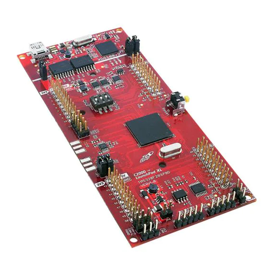
- Page 4 TMS320F2837xD Microcontroller Workshop Required Workshop Materials Required Workshop Materials http://processors.wiki.ti.com/index.php/ C2000_Multi-Day_Workshop F28379D LaunchPad (LAUNCHXL-F28379D) Install Code Composer Studio v7.3.0 Run the workshop installer F2837xD Microcontroller Workshop-2.0-Setup.exe Lab Files / Solution Files Workshop Manual Development Tools F28379D LaunchPad JP3: 5V JP2: GND...
- Page 5 TMS320F2837xD Microcontroller Workshop F28379D controlCARD A:J1 - USB A:SW1 - isolated emulation LED LD2: LED LD3: J8: Host/ emulation/ and UART communication Device GPIO31 (red) GPIO34 (red) UART enable switch U5: µSD card LD1: Power (green) TMS320F28379D SW3: ADC SW2: ADC J2 - J7: USB SW1: Boot VREFHI...
- Page 6 TMS320F2837xD Microcontroller Workshop TMS320F28x7x Device Comparison TMS320F28x7x Device Comparison F2807x F2837xS F2837xD C28x CPUs Clock 120 MHz 200 MHz 200 MHz Flash / RAM / OTP 256Kw / 50Kw / 2Kw 512Kw / 82Kw / 2Kw 512Kw / 102Kw / 2Kw On-chip Oscillators P (each CPU) Watchdog Timer...
- Page 7 TMS320F2837xD Microcontroller Workshop F2837xS – Single-Core Block Diagram F2807x – Block Diagram TMS320F2837xD Microcontroller Workshop - Introduction...
- Page 8 TMS320F2837xD Microcontroller Workshop viii TMS320F2837xD Microcontroller Workshop - Introduction...
-
Page 9: Architecture Overview
Introduction This architectural overview introduces the basic architecture of the C2000™ family of microcontrollers from Texas Instruments. The F28x7x series adds a new level of high performance processing ability. The C2000™ is ideal for applications combining digital signal processing, microcontroller processing, efficient C code execution, and operating system tasks. -
Page 10: Table Of Contents
Introduction to the TMS320F28x7x Chapter Topics Architecture Overview ........................ 1-1 Introduction to the TMS320F28x7x ................... 1-3 C28x Internal Bussing ......................1-4 C28x CPU + FPU + VCU + TMU and CLA ................1-5 Special Instructions ....................... 1-6 CPU Pipeline ......................... 1-7 C28x CPU + FPU + VCU + TMU Pipeline ................ -
Page 11: Introduction To The Tms320F28X7X
Introduction to the TMS320F28x7x Introduction to the TMS320F28x7x The TMS320F37xD, TMS320F37xS, and TMS320F07x, collectively referred to as the TMS320F28x7x or F28x7x, are device members of the C2000™ microcontroller (MCU) product family. These devices are most commonly used within embedded control applications. Even though the topics presented in this workshop are based on the TMS320F2837xD dual-core device series, most all of the topics are fully applicable to the TMS320F2837xS and TMS320F2807x single-core device series. -
Page 12: C28X Internal Bussing
Introduction to the TMS320F28x7x communication peripherals and consists of the multichannel buffered serial port, I2C, SCI, SPI, CAN, and USB. The PIE block, or Peripheral Interrupt Expansion block, manages the interrupts from the peripherals. In the bottom right corner is the general-purpose I/O. The CPU has a watchdog module and three 32-bit general-purpose timers are available. -
Page 13: C28X Cpu + Fpu + Vcu + Tmu And Cla
C28x CPU + FPU + VCU + TMU and CLA C28x CPU + FPU + VCU + TMU and CLA The C28x is a highly integrated, high performance solution for demanding control applications. The C28x is a cross between a general purpose microcontroller and a digital signal processor DSP), balancing the code density of a RISC processor and the execution speed of a DSP with the architecture, firmware, and development tools of a microcontroller. -
Page 14: Special Instructions
C28x CPU + FPU + VCU + TMU and CLA Special Instructions C28x Atomic Read/Modify/Write Atomic Instructions Benefits LOAD Simpler programming READ Smaller, faster code Registers ALU / MPY Uninterruptible (Atomic) WRITE More efficient compiler STORE Standard Load/Store Atomic Read/Modify/Write DINT... -
Page 15: Cpu Pipeline
C28x CPU + FPU + VCU + TMU and CLA CPU Pipeline C28x CPU Pipeline 8-stage pipeline E & G Access same address F1: Instruction Address Protected Pipeline F2: Instruction Content D1: Decode Instruction Order of results are as written in ... -
Page 16: C28X Cpu + Fpu + Vcu + Tmu Pipeline
C28x CPU + FPU + VCU + TMU and CLA C28x CPU + FPU + VCU + TMU Pipeline C28x CPU + FPU + VCU + TMU Pipeline Fetch Decode Read Exe Write F28x Pipeline FPU Instruction VCU / TMU Instruction Load Store 0 delay slot instruction... -
Page 17: Peripheral Write-Read Protection
C28x CPU + FPU + VCU + TMU and CLA Peripheral Write-Read Protection Peripheral Write-Read Protection Suppose you need to write to a peripheral register and then read a different register for the same peripheral (e.g., write to control, read from status register)? CPU pipeline protects W-R order for the same address ... -
Page 18: Memory
Memory Memory The F28x7x MCU utilizes a memory map where the unified memory blocks can be accessed in either program space, data space, or both spaces. This type of memory map lends itself well for supporting high-level programming languages. The memory structure consisting of dedicated RAM blocks, shared local RAM blocks, shared global RAM blocks, message RAM blocks, Flash, and one-time programmable (OTP) memory. -
Page 19: Dual Code Security Module (Dcsm)
Memory factory-default pins cannot be used. This information is programmed into the dual code security module (DCSM). The flash memory is primarily used to store program code, but can also be used to store static data. Notice that the external memory interface is assigned a region within the memory map. -
Page 20: Fast Interrupt Response Manager
Fast Interrupt Response Manager Fast Interrupt Response Manager The fast interrupt response manage is capable of automatically performing context save of critical registers. This results in the ability of servicing many asynchronous events with minimal latency. The F28x7x implements a zero cycle penalty to do 14 registers context saved and restored during an interrupt. -
Page 21: Math Accelerators
Math Accelerators Math Accelerators Viterbi / Complex Math Unit (VCU-II) Viterbi / Complex Math Unit (VCU-II) Extends C28x instruction set to support: VCU-II VCU execution registers Viterbi operations VSTATUS Decode for communications Data path logic for VCU-II Complex math ... -
Page 22: Trigonometric Math Unit (Tmu)
Math Accelerators Trigonometric Math Unit (TMU) Trigonometric Math Unit (TMU) Adds instructions to FPU for calculating common Trigonometric operations x = r * cos(rad) Operation Instruction Exe Cycles Result Latency FPU Cycles w/o TMU Z = Y/X DIVF32 Rz,Ry,Rx Y = sqrt(X) SQRTF32 Ry,Rx Y = sin(X/2pi) -
Page 23: On-Chip Safety Features
On-Chip Safety Features On-Chip Safety Features On-Chip Safety Features Memory Protection ECC and parity enabled RAMs, shared RAMs protection ECC enabled flash memory Clock Checks Missing clock detection logic PLLSLIP detection NMIWDs Windowed watchdog ... -
Page 24: Summary
Summary Summary Summary High performance 32-bit CPU 32x32 bit or dual 16x16 bit MAC IEEE single-precision floating point unit (FPU) Hardware Control Law Accelerator (CLA) Viterbi, complex math, CRC unit (VCU) Trigonometric math unit (TMU) ... - Page 25 Programming Development Environment Introduction This module will explain how to use Code Composer Studio (CCS) integrated development environment (IDE) tools to develop a program. Creating projects and setting building options will be covered. Use and the purpose of the linker command file will be described. Module Objectives Module Objectives Use Code Composer Studio to:...
- Page 26 Code Composer Studio Chapter Topics Programming Development Environment ................2-1 Code Composer Studio ......................2-3 Software Development and COFF Concepts ................ 2-3 Code Composer Studio ......................2-4 Edit and Debug Perspective (CCSv7) ................... 2-5 Target Configuration ......................2-6 CCSv7 Project ........................2-7 Creating a New CCSv7 Project .....................
-
Page 27: Programming Development Environment
Code Composer Studio Code Composer Studio Software Development and COFF Concepts In an effort to standardize the software development process, TI uses the Common Object File Format (COFF). COFF has several features which make it a powerful software development system. It is most useful when the development task is split between several programmers. Each file of code, called a module, may be written independently, including the specification of all resources necessary for the proper operation of the module. - Page 28 Code Composer Studio Writing code in modular form permits code to be developed by several people working in parallel so the development cycle is shortened. Debugging and upgrading code is faster, since components of the system, rather than the entire system, is being operated upon. Also, new systems may be developed more rapidly if previously developed modules can be used in them.
-
Page 29: Edit And Debug Perspective (Ccsv7)
Code Composer Studio Edit and Debug Perspective (CCSv7) A perspective defines the initial layout views of the workbench windows, toolbars, and menus that are appropriate for a specific type of task, such as code development or debugging. This minimizes clutter to the user interface. Edit and Debug Perspective (CCSv7) Each perspective provides a set of functionality aimed ... -
Page 30: Target Configuration
Code Composer Studio Target Configuration A Target Configuration defines how CCS connects to the device. It describes the device using GEL files and device configuration files. The configuration files are XML files and have a *.ccxml file extension. Creating a Target Configuration ... -
Page 31: Ccsv7 Project
Code Composer Studio CCSv7 Project project Code Composer works with a paradigm. Essentially, within CCS you create a project for each executable program you wish to create. Projects store all the information required to build the executable. For example, it lists things like: the source files, the header files, the target system’s memory-map, and program build options. -
Page 32: Creating A New Ccsv7 Project
Code Composer Studio Creating a New CCSv7 Project A graphical user interface (GUI) is used to assist in creating a new project. The GUI is shown in the slide below. Creating a New CCSv7 Project 1. Project Name, Location, and Device ... -
Page 33: Ccsv7 Build Options - Compiler / Linker
Code Composer Studio CCSv7 Build Options – Compiler / Linker Project options direct the code generation tools (i.e. compiler, assembler, linker) to create code according to your system’s needs. When you create a new project, CCS creates two sets of build options –... -
Page 34: Ccs Debug Environment
Code Composer Studio CCS Debug Environment The basic buttons that control the debug environment are located in the top of CCS: The common debugging and program execution descriptions are shown below: Start debugging Image Name Description Availability New Target Creates a new target configartion file. File New Menu Configuration Target Menu... - Page 35 Code Composer Studio Program execution Image Name Description Availability Halt Halts the selected target. The rest of the debug Target Menu views will update automatically with most recent Debug View Toolbar target data. Resumes the execution of the currently loaded Target Menu program from the current PC location.
-
Page 36: Creating A Linker Command File
Creating a Linker Command File Creating a Linker Command File Sections Looking at a C program, you'll notice it contains both code and different kinds of data (global, local, etc.). All code consists of different parts called sections. All default section names begin with a dot and are typically lower case. - Page 37 Creating a Linker Command File The following is a list of the sections that are created by the compiler. Along with their description, we provide the Section Name defined by the compiler. This is a small list of compiler default section names. The top group is initialized sections, and they are linked to flash. In our previous code example, we saw .txt was used for code, and .cinit for initialized values.
- Page 38 Creating a Linker Command File must be declared with a directive to reserve memory to contain its value. By their nature, no value is assigned, instead they are loaded at runtime by the program. Next, we need to place the sections that were created by the compiler into the appropriate memory spaces.
-
Page 39: Linker Command Files (.Cmd)
Creating a Linker Command File Linker Command Files (.cmd) The linker concatenates each section from all input files, allocating memory to each section based on its length and location as specified by the MEMORY and SECTIONS commands in the linker command file. The linker command file describes the physical hardware memory and specifies where the sections are placed in the memory. -
Page 40: Section Placement
Creating a Linker Command File Remember that the MCU has two memory maps: Program, and Data. Therefore, the MEMORY description must describe each of these separately. The loader uses the following syntax to delineate each of these: Linker Page TI Definition Page 0 Program Page 1... -
Page 41: Summary: Linker Command File
Creating a Linker Command File The linker will gather all the code sections from all the files being linked together. Similarly, it will combine all ‘like’ sections. Beginning with the first section listed, the linker will place it into the specified memory segment. Summary: Linker Command File The linker command file (.cmd) contains the inputs —... -
Page 42: Lab File Directory Structure
Lab File Directory Structure Lab File Directory Structure Lab File Directory Structure Supporting Files Easier to make projects portable ${PROJECT_ROOT} provides an anchor point for paths to files that travel with the project Easier to maintain and update ... -
Page 43: Lab 2: Linker Command File
Lab 2: Linker Command File Lab 2: Linker Command File Objective Use a linker command file to link the C program file (Lab2.c) into the system described below. Lab 2: Linker Command File Memory on-chip memory F2837x System Description: •... - Page 44 4. In the next window that appears, select the emulator using the “Connection” pull-down list and choose “Texas Instruments XDS100v2 USB Debug Probe”. In the “Board or Device” box type TMS320F28379D to filter the options. In the box below, check the box to select “TMS320F28379D”.
- Page 45 Lab 2: Linker Command File A CCS Project window will open. At the top of this window, filter the “Target” options by using the pull-down list on the left and choose “2837xD Delfino”. In the pull-down list immediately to the right, choose the “TMS320F28379D”. Leave the “Connection”...
- Page 46 Lab 2: Linker Command File cla1, the “Specify floating point support” is set to fpu32, the “Specify TMU support” is set to TMU0, and the “Specify VCU support” is set to vcu2. Select OK to close the Properties window. Linker Command File – Lab2.cmd 16.
- Page 47 Lab 2: Linker Command File Debug Environment Windows It is standard debug practice to watch local and global variables while debugging code. There are various methods for doing this in Code Composer Studio. We will examine two of them here: memory browser, and expressions.
- Page 48 Lab 2: Linker Command File 2 - 24 TMS320F2837xD Microcontroller Workshop - Programming Development Environment...
- Page 49 Peripherial Registers Header Files Introduction The purpose of the F2837xD C-code header files is to simplify the programming of the many peripherals on the F28x device. Typically, to program a peripheral the programmer needs to write the appropriate values to the different fields within a control register. In its simplest form, the process consists of writing a hex value (or masking a bit field) to the correct address in memory.
- Page 50 Register Programming Model Chapter Topics Peripherial Registers Header Files .................... 3-1 Register Programming Model ....................3-3 Traditional and Structure Approach to C Coding ..............3-5 Naming Conventions ......................... 3-9 F2837xD C-Code Header Files ....................3-11 Peripheral Structure .h File ....................3-11 Global Variable Definitions File ...................
-
Page 51: Register Programming Model
Register Programming Model Register Programming Model Register Programming Model DriverLib Software C functions automatically set register bit fields Common tasks and DriverLib peripheral modes supported Reduces learning curve and simplifies programming Bit Fields Bit Field Header Files ... - Page 52 Register Programming Model Programming Model Comparison Register addresses # defined individually Direct Register Access User must compute bit-field masks Not easy-to-read *CMPR1 = 0x1234; Header files define all registers as structures Bit Field Header Files Bit-fields directly accessible ...
-
Page 53: Traditional And Structure Approach To C Coding
Traditional and Structure Approach to C Coding Traditional and Structure Approach to C Coding Traditional Approach to C Coding #define TBCTL (volatile unsigned int *)0x00004000 void main(void) *TBCTL = 0x1234; //write entire register *TBCTL |= 0x0003; //stop time-base counter Advantages - Simple, fast and easy to type - Variable names can match register names (easy to remember) - Page 54 Traditional and Structure Approach to C Coding Structure Approach to C Coding void main(void) EPwm1Regs.TBCTL.all = 0x1234; //write entire register EPwm1Regs.TBCTL.bit.CTRMODE = 3; //stop time-base counter Advantages - Easy to manipulate individual bits - Watch window is amazing! (next slide) - Generates most efficient code (on C28x) Disadvantages - Can be difficult to remember the structure names...
- Page 55 Traditional and Structure Approach to C Coding Built-in Register Window Register values can be viewed using the built-in Register Window. Also, the peripheral can be added to the expression window. In addition to viewing register values, individual bit fields can be modified.
- Page 56 Traditional and Structure Approach to C Coding Is the Structure Approach Efficient? The structure approach enables efficient compiler use of DP addressing mode and C28x atomic operations C Source Code Generated Assembly Code* // Stop CPU Timer0 MOVW DP, #0030 CpuTimer0Regs.TCR.bit.TSS = 1;...
-
Page 57: Naming Conventions
Naming Conventions Naming Conventions The header files use a familiar set of naming conventions. They are consistent with the Code Composer Studio configuration tool, and generated file naming conventions. Structure Naming Conventions The F2837xD header files define: All of the peripheral structures ... - Page 58 Naming Conventions Editor Auto Complete to the Rescue! The editor auto complete feature works as follows. First, you type EPwm1Regs. Then, when you type a “.” a window opens up, allowing you to select a control register. In this example TBCTL is selected.
-
Page 59: F2837Xd C-Code Header Files
F2837xD C-Code Header Files F2837xD C-Code Header Files The F2837xD header file package contains everything needed to use the structure approach. It defines all the peripheral register bits and register addresses. The header file package includes the header files, linker command files, code examples, and documentation. The header file package is available from C2000Ware. - Page 60 F2837xD C-Code Header Files Peripheral Structure .h files (1 of 2) Contain bits field structure definitions for each peripheral register F2837xD_epwm.h // EPWM Individual Register Bit Definitions: struct TBCTL_BITS { // bits description Uint16 CTRMODE:2; // 1:0 Counter Mode Uint16 PHSEN:1;...
-
Page 61: Global Variable Definitions File
F2837xD C-Code Header Files three steps needed to use the header files. The first step is to include this file directly or indirectly in each source files. Global Variable Definitions File With F2837xD_GlobalVariableDefs.c included in the project all the needed variable definitions are globally defined. -
Page 62: Mapping Structures To Memory
F2837xD C-Code Header Files Mapping Structures to Memory The data structures describe the register set in detail. And, each instance of the data type (i.e., register set) is unique. Each structure is associated with an address in memory. This is done by (1) creating a new section name via a DATA_SECTION pragma, and (2) linking the new section name to a specific memory in the linker command file. -
Page 63: Peripheral Specific Routines
F2837xD C-Code Header Files Peripheral Specific Routines Peripheral Specific C functions are used to initialize the peripherals. They are used by adding the appropriate .c file to the project. Peripheral Specific Examples Example projects for each peripheral Helpful to get you started ... -
Page 64: Summary
Summary Summary Peripheral Register Header Files Summary Easier code development Easy to use Generates most efficient code Increases effectiveness of CCS watch window TI has already done all the work! Use the correct header file package for your device: ... - Page 65 Reset and Interrupts Introduction This module covers the interrupt process and explains how the Peripheral Interrupt Expansion (PIE) is used to service the peripheral interrupts. Module Objectives Module Objectives Describe the F28x reset process List the event sequence during an ...
- Page 66 Reset and Boot Process Chapter Topics Reset and Interrupts ........................4-1 Reset and Boot Process ......................4-3 Reset - Bootloader ........................ 4-5 Emulation Boot Mode ......................4-6 Stand-Alone Boot Mode ......................4-7 Reset Code Flow – Summary ....................4-8 Emulation Boot Mode using Code Composer Studio GEL ........... 4-8 Getting to main() ........................
-
Page 67: Reset And Boot Process
Reset and Boot Process Reset and Boot Process Reset Sources Missing Clock Detect F28x7x Watchdog Timer * Power-on Reset Hibernate Reset XRS pin active To XRS pin * = CPU1.WD resets both cores and Logic shown is functional representation, not actual implementation CPU2.WD resets CPU2 only POR –... - Page 68 Reset and Boot Process Dual-Core Boot Process CPU1 starts execution from CPU1 boot ROM while CPU2 is held in reset CPU1 controls the boot process CPU2 goes through its own boot process under the control of CPU1 – except when CPU2 is set to boot-to-flash IPC registers are used to communicate ...
-
Page 69: Reset - Bootloader
Reset and Boot Process Reset - Bootloader Reset – Bootloader Reset vector Reset fetched from boot ROM CPU2 held in ENPIE = 0 reset until INTM = 1 0x3F FFC0 released by CPU1. CPU2 Emulator Connected ? TRST = 1 TRST = 0 Emulation Boot Stand-alone Boot... -
Page 70: Emulation Boot Mode
Reset and Boot Process Emulation Boot Mode Emulation Boot Mode (TRST = 1) slide 1 of 2 Emulator Connected Emulation Boot If either EMU_KEY or EMU_BMODE are invalid, the “wait” boot mode is Boot determined by used. These values can then be EMU_BOOTCTRL : modified using the debugger and a reset issued to restart the boot process. -
Page 71: Stand-Alone Boot Mode
Reset and Boot Process process. This is the typical sequence followed during device power-up with the emulator con- nected, allowing the user to control the boot process using the debugger. Once the EMU_KEY bit fields are set to 0x5A, then the EMU_BMODE bit field values determines the boot mode. -
Page 72: Reset Code Flow - Summary
Reset and Boot Process Reset Code Flow – Summary In summary, the reset code flow is as follows. After reset, the program counter is set to 0x3FFFC0, where the flow is vectored to the Init_Boot code in the Boot ROM. The Init_Boot code defines the execution entry based on emulation boot mode or stand-alone boot mode. -
Page 73: Getting To Main()
Reset and Boot Process Getting to main() After reset how do we get to main() ? At the code entry point, branch to _c_int00() Part of compiler runtime support library Sets up compiler environment Calls main() .sect “codestart”... -
Page 74: Peripheral Software Reset Registers
Reset and Boot Process Peripheral Software Reset Registers Peripheral Software Reset Registers DevCfgRegs.SOFTPRESx.bit.PeripheralName = 1 Peripheral Software Reset Signal Peripheral 0 = controlled by normal CPU reset 1 = reset peripheral (default) Register PeripheralName SOFTPRES0 CPU1_CLA1, CPU2_CLA1 SOFTPRES1 EMIF1, EMIF2 SOFTPRES2 EPWM1, EPWM2, EPWM3, EPWM4, EPWM5, EPWM6, EPWM7, EPWM8, EPWM9, EPWM10, EPWM11, EPWM12 SOFTPRES3... -
Page 75: Interrupts
Interrupts Interrupts Interrupt Sources Internal Sources TINT2 F28x CORE TINT1 TINT0 ePWM, eCAP, eQEP, INT1 ADC, SCI, SPI, I2C, (Peripheral CAN, McBSP, INT2 Interrupt DMA, CLA, WD INT3 Expansion) • • • External Sources INT12 INT13 XINT1 – XINT5 INT14 The internal interrupt sources include the general purpose timers 0, 1, and 2, and all of the peripherals on the device. -
Page 76: Interrupt Processing
Interrupts Interrupt Processing Maskable Interrupt Processing Conceptual Core Overview Core (IFR) (IER) (INTM) Interrupt “Latch” “Switch” “Global Switch” INT1 INT2 F28x Core INT14 A valid signal on a specific interrupt line causes the latch to display a “1” in the appropriate bit If the individual and global switches are turned “on”... -
Page 77: Interrupt Flag Register (Ifr)
Interrupts Interrupt Flag Register (IFR) Interrupt Flag Register (IFR) RTOSINT DLOGINT INT14 INT13 INT12 INT11 INT10 INT9 INT8 INT7 INT6 INT5 INT4 INT3 INT2 INT1 Pending : Absent : /*** Manual setting/clearing IFR ***/ extern cregister volatile unsigned int IFR; IFR |= 0x0008;... -
Page 78: Interrupt Global Mask Bit (Intm)
Interrupts Interrupt Global Mask Bit (INTM) Interrupt Global Mask Bit Bit 0 INTM INTM used to globally enable/disable interrupts: Enable: INTM = 0 Disable: INTM = 1 (reset value) INTM modified from assembly code only: /*** Global Interrupts ***/ asm(“... - Page 79 Interrupts interrupt lines (INT1 through INT12) are used to service the peripheral interrupts. A Peripheral Interrupt Expansion (PIE) module multiplexes up to sixteen peripheral interrupts into each of the twelve CPU interrupt lines, further expanding support for up to 192 peripheral interrupt signals. The PIE module also expands the interrupt vector table, allowing each unique interrupt signal to have its own interrupt service routine (ISR), permitting the CPU to support a large number of peripherals.
- Page 80 Interrupts F2837xD PIE Assignment Table - Upper INTx.16 INTx.15 INTx.14 INTx.13 INTx.12 INTx.11 INTx.10 INTx.9 INT1 IPC3 IPC2 IPC1 IPC0 PWM12_ PWM11_ PWM10_ PWM9_ INT2 INT3 EPWM12 EPWM11 EPWM10 EPWM9 INT4 INT5 INT6 SPIC_TX SPIC_RX INT7 INT8 UPPA INT9 USBA ADCD_ ADCC_ INT10...
-
Page 81: Pie Block Initialization
Interrupts PIE Block Initialization PIE Block Initialization Memory Map Main.c // CPU Initialization • • • InitPieCtrl(); • • • PIE RAM Vectors 512w PieVect.c PieCtrl.c (ENPIE = 1) PIE_VECT_TABLE // Initialize PIE_RAM • • // Base Vectors • • memcpy( •... - Page 82 Interrupts PIE Initialization Code Flow - Summary RESET Reset Vector Boot option determines code execution entry point <0x3F FFC0> <reset vector> = Boot Code CodeStartBranch.asm .sect “codestart” M0 RAM Entry Point Flash Entry Point <0x00 0000> = LB _c_int00 <0x08 0000> = LB _c_int00 rts2800_fpu32.lib _c_int00: Interrupt...
-
Page 83: Interrupt Signal Flow - Summary
Interrupts Interrupt Signal Flow – Summary Interrupt Signal Flow – Summary Peripheral Interrupt Expansion (PIE) – Interrupt Group PIEIFRx PIEIERx INTx.y Peripheral Interrupt PieCtrlRegs.PIEIERx.bit.INTxy = 1; Core Interrupt Logic Core INTM INTx asm(“ CLRC INTM”); IER |= 0x0001; 0x0FFF; PIE Vector Table DefaultIsr.c interrupt void name(void) -
Page 84: F2837Xd Dual-Core Interrupt Structure
Interrupts F2837xD Dual-Core Interrupt Structure F2837xD Dual-Core Interrupt Structure Internal Sources TINT2.1 CPU1 CORE TINT1.1 DMA1.1 CLA1.1 TINT0.1 INT1 ePWM, eCAP, eQEP, INT2 ADC, SCI, SPI, I2C, INT3 • CAN, McBSP, WD • ePIE.1 • INT12 External Sources INT13 XINT1 – XINT5 INT14 CPU2 CORE INT1... -
Page 85: Interrupt Response And Latency
Interrupts Interrupt Response and Latency Interrupt Response - Hardware Sequence CPU Action Description Registers → stack 14 Register words auto saved 0 → IFR (bit) Clear corresponding IFR bit 0 → IER (bit) Clear corresponding IER bit 1 → INTM/DBGM Disable global ints/debug events Vector →... - Page 86 Interrupts 4 - 22 TMS320F2837xD Microcontroller Workshop - Reset and Interrupts...
- Page 87 System Initialization Introduction This module covers the operation of the OSC/PLL-based clock module and watchdog timer. Also, the general-purpose digital I/O, external interrups, low power modes and the register protection will be covered. Module Objectives Module Objectives OSC/PLL Clock Module ...
- Page 88 Oscillator/PLL Clock Module Chapter Topics System Initialization ........................5-1 Oscillator/PLL Clock Module ..................... 5-3 F2837xD Dual-Core System Clock ..................5-5 Watchdog Timer ........................5-7 General Purpose Digital I/O ....................5-12 GPIO Input X-Bar ........................ 5-15 GPIO Output X-Bar ......................5-16 External Interrupts ........................
-
Page 89: Oscillator/Pll Clock Module
Oscillator/PLL Clock Module Oscillator/PLL Clock Module F28x7x Oscillator / PLL Clock Module Internal OSC1CLK OSC 1 WDCLK (10 MHz) OSCCLKSRCSEL SYSCLKDIV Internal OSC2CLK OSCCLK OSC 2 (PLL bypass) (10 MHz) PLLSYSCLK XCLKIN PLLCLK (X2 n.c.) EXTCLK SYSPLLCTL1 SYSPLLMULT XCLKOUTSEL XCLKOUTDIV AUXPLLCLK CPU2.SYSCLK XCLKOUT... - Page 90 Oscillator/PLL Clock Module F28x7x PLL and LOSPCP ClkCfgRegs.SYSCLKDIVSEL.bit.PLLSYSCLKDIV OSCCLK (PLL bypass) PLLSYSCLK CPUx.SYSCLK CPUx PLLCLK CPUx.LSPCLK LOSPCP ClkCfgRegs.SYSPLLCTL1.bit.PLLCLKEN ClkCfgRegs.SYSPLLMULT.bit.IMULT ClkCfgRegs.LOSPCP.bit.LSPCLK ClkCfgRegs.SYSPLLMULT.bit.FMULT SYSPLL IMULT CLKIN LSPCLK Peripheral Clk Freq 0 0 0 CPUx.SYSCLK / 1 DIVSEL 0 0 0 0 0 0 0 OSCCLK / n * (PLL bypass) 0 0 1 CPUx.SYSCLK / 2 0 0 0 0 0 0 1 OSCCLK x 1 / n...
-
Page 91: F2837Xd Dual-Core System Clock
Oscillator/PLL Clock Module F2837xD Dual-Core System Clock F2837xD Dual-Core System Clock LSPCLKDIV CPU2 CPU2.SYSCLK CPU2.LSPCLK LOSPCP PLLSYSCLK CPU1.SYSCLK CPU1.LSPCLK LOSPCP CPU1 PERx.SYSCLK PERx.LSPCLK SCIx CPUSELy PERx /1, /2 PERx PERx SPIx Peripherals McBSPx EPWMCLK PERCLKDIVSEL EPWM CPU2.TMR2CLKCTL EPWMCLKDIV CPU2.SYSCLK INTOSC1 WD.2 INTOSC2 EXTCLK... - Page 92 Oscillator/PLL Clock Module Dual-Core CPU Select Registers DevCfgRegs.CPUSELx.bit.PeripheralName = 0 CPU1.SYSCLK Peripheral CPU2.SYSCLK 0 = connected to CPU1 1 = connected to CPU2 (default) Note: CPUSELx must be configured before PCLKCRx Register PeripheralName CPUSEL0 EPWM1, EPWM2, EPWM3, EPWM4, EPWM5, EPWM6, EPWM7, EPWM8, EPWM9, EPWM10, EPWM11, EPWM12 CPUSEL1 ECAP1, ECAP2, ECAP3, ECAP4, ECAP5, ECAP6 CPUSEL2...
-
Page 93: Watchdog Timer
Watchdog Timer Watchdog Timer The watchdog timer is a safety feature, which resets the device if the program runs away or gets trapped in an unintended infinite loop. The watchdog counter runs independent of the CPU. If the counter overflows, a user-selectable reset or interrupt is triggered. During runtime the correct key values in the proper sequence must be written to the watchdog key register in order to reset the counter before it overflows. - Page 94 Watchdog Timer Watchdog Timer Module WDOVERRIDE WDPS Watchdog WDCLK /512 Prescaler WDDIS WDCNTR 8-bit Watchdog Counter WDRST System Output Reset Pulse WDCNTR WDWCR WDINT less than WDWCR window 55 + AA minimum Detector Good Key WDCHK Watchdog Reset Key Register Bad WDCHK Key WDKEY 1 0 1...
- Page 95 Watchdog Timer Watchdog Period Selection WDPS WD timeout period Bits rollover @ 10 MHz WDCLK 00x: 13.11 ms * 010: 26.22 ms 011: 52.44 ms 100: 104.88 ms 101: 209.76 ms 110: 419.52 ms 111: 839.04 ms * reset default Remember: Watchdog starts counting immediately after ...
- Page 96 Watchdog Timer Resetting the Watchdog SysCtrlRegs.WDKEY (lab file: Watchdog.c) 15 - 8 7 - 0 reserved WDKEY WDKEY write values: 55h - counter enabled for reset on next AAh write AAh - counter set to zero if reset enabled Writing any other value has no effect ...
- Page 97 Watchdog Timer System Control and Status Register SysCtrlRegs.SCSR (lab file: Watchdog.c) WD Override (protect bit) Protects WD from being disabled 0 = WDDIS bit in WDCR has no effect (WD cannot be disabled) 1 = WDDIS bit in WDCR can disable the watchdog •...
-
Page 98: General Purpose Digital I/O
General Purpose Digital I/O General Purpose Digital I/O F28x7x GPIO Grouping Overview GPIO Port A Group GPIO Port A Mux1 Mux1 Register Register Input (GPAGMUX1) (GPAMUX1) GPIO Port A Qual [GPIO 0 to 15] [GPIO 0 to 15] Direction Register (GPADIR) GPIO Port A Group GPIO Port A Mux2... - Page 99 General Purpose Digital I/O F2837xD GPIO Pin Block Diagram unused 00:00 Input CPU2.CLA CPU2 CPU1.CLA CPU1 00:01 Peripheral 1 X-BAR GPxDAT(R GPxDAT(R GPxDAT(R GPxDAT(R 00:10 Peripheral 2 00:11 Peripheral 3 unused Input 01:00 01:01 Peripheral 5 Qualification CPU1 01:10 Peripheral 6 GPxCSEL1-4 01:11 Peripheral 7...
- Page 100 General Purpose Digital I/O F28x7x GPIO Input Qual Registers GpioCtrlRegs.register (lab file: Gpio.c) GPxQSEL1 / GPxQSEL2 where x = A, B, C, D, E or F 16 pins configured per register 00 = sync to SYSCLKOUT only * 01 = qual to 3 samples 10 = qual to 6 samples 11 = no sync or qual (for peripheral only;...
-
Page 101: Gpio Input X-Bar
General Purpose Digital I/O F28x7x GPIO Control & Data Registers GpioCtrlRegs.register / GpioDataRegs.register (lab file: Gpio.c) Register Description GPxCTRL GPIO x Control Register GPxQSEL1 GPIO x Qualifier Select 1 Register GPxQSEL2 GPIO x Qualifier Select 2 Register GPxMUX1 GPIO x Mux1 Register GPxMUX2 GPIO x Mux2 Register GPxDIR... -
Page 102: Gpio Output X-Bar
General Purpose Digital I/O above the multiplexing scheme used by the GPIO structure. Since the GPIO does not affect the Input X-BAR, it is possible to route the output of one peripheral to another, such as measuring the output of an ePWM with an eCAP for frequency testing. F28x7x GPIO Input X-Bar Architecture This block diagram is replicated 14 times GPIO 0... - Page 103 General Purpose Digital I/O The Output X-BAR is used to route various internal signals out of the device. It contains eight outputs that are routed to the GPIO structure, where each output has one or multiple assigned pin positions, which are labeled as OUTPUTXBARx. Additionally, the Output X-BAR can select a single signal or logically OR up to 32 signals.
-
Page 104: External Interrupts
External Interrupts External Interrupts External Interrupts 5 external interrupt signals: XINT1, XINT2, XINT3, XINT4 and XINT5 Each can be mapped to any of GPIO pins via the X-Bar Input architecture XINT1, XINT2 and XINT3 also each have a ... -
Page 105: Low Power Modes
Low Power Modes Low Power Modes Low Power Modes Low Power CPU Logic Watchdog PLL / Peripheral Mode Clock Clock Logic Clock Normal Run IDLE STANDBY HALT HIB * * Hibernate - low power data retention via M0 and M1 memories See device datasheet for power consumption in each mode Low Power Mode Control Register SysCtrlRegs.LPMCR (lab file: SysCtrl.c) - Page 106 Low Power Modes Low Power Mode Exit Exit GPIO Interrupt Watchdog Port A Enabled RESET Interrupt Low Power Signal Interrupt Mode IDLE STANDBY HALT * Hibernate - GPIO41 becomes HIBWAKE reset signal; boot ROM avoids clearing M0 and M1 memories and calls a user-specified IO restore function GPIO Low Power Wakeup Select SysCtrlRegs.GPIOLPMSELx GPIO63...
-
Page 107: Register Protection
Register Protection Register Protection LOCK Protection Registers “LOCK” registers protects several system configuration registers from spurious CPU writes Once LOCK register bits are set the respective locked registers can no longer be modified by software CLA1TASKSRCSELLOCK Z2_OTPSECLOCK GPELOCK DMACHSRCSELLOCK DxLOCK GPFLOCK... - Page 108 Register Protection EALLOW Protection (2 of 2) The following registers are protected: Device Configuration & Emulation Flash Code Security Module PIE Vector Table DMA, CLA, SD, EMIF, X-Bar (some registers) CANA/B (control registers only; mailbox RAM not protected) ePWM, CMPSS, ADC, DAC (some registers) GPIO (control registers only) System Control See device datasheet and Technical Reference Manual for detailed listings...
-
Page 109: Lab 5: System Initialization
Lab 5: System Initialization Lab 5: System Initialization Objective The objective of this lab exercise is to perform the processor system initialization. Additionally, the peripheral interrupt expansion (PIE) vectors will be initialized and tested using the information discussed in the previous module. This initialization process will be used again in all of the lab exercises throughout this workshop. - Page 110 Lab 5: System Initialization Project Build Options 3. Setup the build options by right-clicking on Lab5 in the Project Explorer window and select “Properties”. We need to setup the include search path to include the peripheral register header files and common lab header files. Under “C2000 Compiler” select “Include Options”.
- Page 111 Lab 5: System Initialization Build and Load 10. Click the “Build” button and watch the tools run in the Console window. Check for errors in the Problems window. 11. Click the “Debug” button (green bug). A Launching Debug Session window will open. Select only CPU1 to load the program on (i.e.
- Page 112 Lab 5: System Initialization EMU_BMODE values from the PIE RAM. These values were previously set for boot to RAMM0 boot mode by CCS. Since these values did not change and are not affected by reset, the bootloader transferred execution to the beginning of our code at address 0x000000 in the RAMM0, and execution continued until the breakpoint was hit in main( ).
- Page 113 Lab 5: System Initialization Setup PIE Vector for Watchdog Interrupt The first part of this lab exercise used the watchdog to generate a CPU reset. This was tested using a breakpoint set at the beginning of main(). Next, we are going to use the watchdog to generate an interrupt.
- Page 114 Lab 5: System Initialization Run the Code – Watchdog Interrupt 31. Place the cursor in the “main loop” section, right click the mouse key and select Run To Line. 32. Run your code. Where did your code stop? Are the results as expected? If things went as expected, your code should stop at the “ESTOP0”...
- Page 115 Analog Subsystem Introduction The Analog Subsystem consists of the Analog-to-Digital Converter (ADC), Comparator Subsystem (CMPSS), Digital-to-Analog Converter (DAC), and the Sigma Delta Filter Module (SDFM). This module will explain the operation of each subsystem. Even though the SDFM is a digital peripheral, it will be covered in this module.
- Page 116 Analog-to-Digital Converter (ADC) 6 - 2 TMS320F2837xD Microcontroller Workshop - Analog Subsystem...
- Page 117 Analog-to-Digital Converter (ADC) Chapter Topics Analog Subsystem ........................6-1 Analog-to-Digital Converter (ADC) .................... 6-4 ADC Block and Functional Diagrams ..................6-5 ADC Triggering ........................6-7 ADC Conversion Priority ....................... 6-8 Post Processing Block ......................6-11 ADC Clocking Flow ......................6-14 ADC Registers ........................
- Page 118 Analog-to-Digital Converter (ADC) Analog-to-Digital Converter (ADC) ADC Subsystem VREFA VREFC DACOUTA/ADCINA0 Reserved DACOUTB/ADCINA1 Reserved CMPIN1P/ADCINA2 CMPIN6P/ADCINC2 CMPIN1N/ADCINA3 CMPIN6N/ADCINC3 CMPIN2P/ADCINA4 CMPIN5P/ADCINC4 CMPIN2N/ADCINA5 CMPIN5N/ADCINC5 Reserved Reserved ADC-A ADC-C Reserved Reserved 16/12-bit 16/12-bit VREFLOA VREFLOC 16 channel 16 channel VREFLOA VREFLOC Reserved Reserved Reserved Reserved DACOUTA...
-
Page 119: Analog-To-Digital Converter (Adc)
Analog-to-Digital Converter (ADC) ADC Block and Functional Diagrams ADC Module Block Diagram ADCIN0 ADCRESULT0 ADCIN1 ADCRESULT1 ADCIN2 12/16-bit Result ADCIN3 ADCRESULT2 Converter SOCx ADCIN14 ADCRESULT15 ADCIN15 ADC full-scale EOCx ADCINT1-4 CHSEL input range is Interrupt Generation to V Logic Logic REFLO REFHI SOCx Signal... - Page 120 Analog-to-Digital Converter (ADC) ADC SOCx Functional Diagram TINT0 (CPU1 Timer 0) ADCSOCxCTL TINT1 (CPU1 Timer 1) TINT2 (CPU1 Timer 2) ADCEXTSOC (GPIO) ADCRESULTx SOCA/C (ePWM1) ADCINT1 SOCB/D (ePWM1) Channel Sample Result ADCINT2 ADCINT3 Select Window Register SOCA/C (ePWM12) ADCINT4 SOCB/D (ePWM12) TINT0 (CPU2 Timer 0) TINT1 (CPU2 Timer 1) TINT2 (CPU2 Timer 2)
-
Page 121: Adc Triggering
Analog-to-Digital Converter (ADC) ADC Triggering Example – ADC Triggering Sample A1 A5 when ePWM1 SOCB/D is generated and then generate ADCINT1: Channel Sample SOC0 Result0 no interrupt SOCB/D (ETPWM1) 20 cycles SOC1 Channel Sample Result1 no interrupt 26 cycles SOC2 Channel Sample... -
Page 122: Adc Conversion Priority
Analog-to-Digital Converter (ADC) The ADC ping-pong triggering example in the figure above shows channels B0 through B5 being converted, triggered initially by software. After channel B2 is converted, ADCINT1 is generated, which also triggers channel B3. After channel B5 is converted, ADCINT2 is generated and is also fed back to start the process again from the beginning. - Page 123 Analog-to-Digital Converter (ADC) Conversion Priority Functional Diagram SOC0 SOC Priority SOC1 Determines cutoff point SOC2 for high priority and SOC3 round robin mode SOC4 SOCPRIORITY SOC5 SOC6 AdcRegs.SOCPRICTL SOC7 RRPOINTER SOC8 SOC9 Round Robin Pointer SOC10 Points to the last converted SOC11 round robin SOCx and SOC12...
- Page 124 Analog-to-Digital Converter (ADC) High Priority Example SOCPRIORITY configured as 4; RRPOINTER configured as 15; SOC4 is highest RR priority High Priority SOC7 trigger received SOC7 is converted; RRPOINTER points to SOC7; SOC8 is now highest RR priority RRPOINTER SOC2 & SOC12 triggers received simultaneously SOC2 is converted;...
- Page 125 Analog-to-Digital Converter (ADC) Round Robin Burst Mode with High Priority Example SOCPRIORITY configured as 4; RRPOINTER configured as 15; SOC4 is highest RR priority High Priority BURSTTRIG trigger received SOC4 & SOC5 is converted; RRPOINTER points to SOC5; SOC6 is now highest RR priority RRPOINTER BURSTTRIG &...
- Page 126 Analog-to-Digital Converter (ADC) Post Processing Block - Diagram Delay Capture ADCEVTSEL.PPBxTRIPLO SOC Control Signals ADCEVTSEL.PPBxTRIPHI Trigger Start Detect Detect ADCEVTSEL.PPBxZERO latch latch ADCEVTSTAT.PPBxTRIPLO Σ REQSTAMPx DLYSTAMPx EVENTx FREECOUNT ADCEVTSTAT.PPBxTRIPHI ADCEVTSTAT.PPBxZERO Offset Correction w/ Saturation ADCPPBxOFFCAL Threshold Compare Zero ADC Output saturate Crossing Σ...
-
Page 127: Post Processing Block 1
Analog-to-Digital Converter (ADC) Post Processing Block Interrupt Event Each ADC module contains four (4) Post Processing Blocks Each Post Processing Block can be associated with any of the 16 ADCRESULTx registers Post Processing Block 1 EVENTx ADCEVT1 INTx Post Processing Block 2 EVENTx ADCEVT2... -
Page 128: Adc Clocking Flow
Analog-to-Digital Converter (ADC) ADC Clocking Flow ADC Clocking Flow Internal SYSPLLMULT SYSCLKDIVSEL SYSCLK PLL out (200 MHz) (400 MHz) (10 MHz) FMULT/IMULT PLLSYSCLKDIV bits To CPU bits 10b (/2) 00|0|101000b (x40) PCLKCR13.ADC_A = 1 ADCCTL2 PRESCALE ADCCLK (50 MHz) To ADC core bits ADCSOCxCTL 0110b (/4) - Page 129 Analog-to-Digital Converter (ADC) ADC Control Register 1 AdczRegs.ADCCTL1 (z = a, b, c, or d) INT Pulse Generation Control ADC Busy ADC Busy Channel 0 = beginning of 0 = ADC available When ADCBSY = conversion 1 = ADC busy 0: last channel converted 1 = one cycle prior 1: channel currently processing...
- Page 130 Analog-to-Digital Converter (ADC) ADC SOC0 – SOC15 Control Registers AdczRegs.ADCSOCxCTL (z = a, b, c, or d) SOCx Trigger SOCx Channel SOCx Acquisition Source Select Select Prescale (S/H window) 31 - 25 24 - 20 18 - 15 14 - 9 8 - 0 reserved TRIGSEL...
- Page 131 Analog-to-Digital Converter (ADC) SOC Priority Control Register AdczRegs.SOCPRICTL (z = a, b, c, or d) 15 - 10 9 - 5 4 - 0 reserved RRPOINTER SOCPRIORITY Round Robin Pointer SOC Priority Points to the last converted Determines cutoff point round robin SOCx and for high priority and determines order...
- Page 132 Analog-to-Digital Converter (ADC) Interrupt Select x and y Register AdczRegs.INTSELxNy (z = a, b, c, or d) Where x/y = 1/2, 3/4 11 - 8 reserved INTyCONT INTyE reserved INTySEL 3 - 0 reserved INTxCONT INTxE reserved INTxSEL ADCINTx/y EOC Source Select 00h = EOC0 is trigger for ADCINTx/y ADCINTx/y ADCINTx/y...
-
Page 133: Signed Input Voltages
Analog-to-Digital Converter (ADC) ADC Conversion Result Registers 16-Bit Mode AdcnResultRegs.ADCRESULTx n = a - d x = 0 - 15 ADCINxP ADCINxN Digital AdcnResultRegs. Voltage Voltage Results ADCRESULTx 3.0V FFFFh 1111|1111|1111|1111 1.5V 1.5V 7FFFh 0111|1111|1111|1111 45µV 3.0V - 45µV 0000|0000|0000|0001 3.0V 0000|0000|0000|0000 Differential –... -
Page 134: Adc Calibration And Reference
Analog-to-Digital Converter (ADC) ADC Calibration and Reference Built-In ADC Calibration TI reserved OTP contains device specific calibration data for the ADC, internal oscillators and buffered DAC The Boot ROM contains a Device_cal() routine that copies the calibration data to their respective registers Device_cal() must be run to meet the specifications in ... - Page 135 Analog-to-Digital Converter (ADC) Analog Subsystem External Reference Reference Generation Non-Inverting Buffers Voltage VREFHIA Reference VREFLOA REF3230 VREFHIB REF3225 VREFLOB REF3030 REF3025 VREFHIC (or similar) VREFLOC VREFHID VREFLOD TMS320F2837xD Microcontroller Workshop - Analog Subsystem 6 - 21...
-
Page 136: Comparator Subsystem (Cmpss)
Comparator Subsystem (CMPSS) Comparator Subsystem (CMPSS) Comparator Subsystem Eight Comparator Subsystems (CMPSS) Each CMPSS has: CMPIN1P/ADCINA2 CMPIN1N/ADCINA3 CMPIN2P/ADCINA4 Two analog comparators ADC-A CMPIN2N/ADCINA5 CMPIN4P/ADCIN14 Two programmable 12-bit CMPIN4N/ADCIN15 DACs CMPIN3P/ADCINB2 ADC-B CMPIN3N/ADCINB3 Two digital filters ... -
Page 137: Comparator Subsystem Block Diagram
Comparator Subsystem (CMPSS) Comparator Subsystem Block Diagram Comparator Subsystem Block Diagram CTRIPH CMPINxP COMPDACE to EPwm X-Bar COMPH Digital Filter DACH VALS 12-bit DACH ePWM CTRIPOUTH VALA COMPHINV to Output Event X-Bar COMPHSOURCE Trigger & DACSOURCE CTRIPL GPIO to EPwm X-Bar CMPINxN COMPL... -
Page 138: Digital-To-Analog Converter (Dac)
Digital-to-Analog Converter (DAC) Digital-to-Analog Converter (DAC) Digital-to-Analog Converter DACOUTA/ADCINA0 DACOUTB/ADCINA1 Three buffered 12-bit DACs ADC-A DACOUTA Provides a programmable reference output voltage DACOUTC/ADCINB1 ADC-B DACOUTA Capable of driving an external load ADC-C Ability to be synchronized DACOUTA with PWMSYNC events Selectable reference voltage... -
Page 139: Buffered Dac Block Diagram
Digital-to-Analog Converter (DAC) Buffered DAC Block Diagram Buffered DAC Block Diagram DACREFSEL REFHI DACOUTEN 12-bit DACV DACV DACOUT Ideal Output VREFHIA can supply reference DACVALA * DACREF for DAC A and DAC B; VREFHIB DACOUT 4096 can supply reference for DAC C Note: registers lock protected Two sets of DACVAL registers are present in the buffered DAC module: DACVALA and DACVALS. -
Page 140: Sigma Delta Filter Module (Sdfm)
Sigma Delta Filter Module (SDFM) Sigma Delta Filter Module (SDFM) Sigma Delta Filter Module (SDFM) SDFM is a four-channel digital filter designed specifically for current measurement and resolver position decoding in motor control applications Each channel can receive an independent modulator ... -
Page 141: Sdfm Block Diagram
Sigma Delta Filter Module (SDFM) SDFM Block Diagram SDFM Block Diagram CMPC/D SDFM- Sigma Delta Filter Module SDFILRESn Sync ΣΔ Clk_out Filter Module 1 Streams Direct SDINT Comparator Interrupt Filter Unit Input CLK1 Ctrl FILRES Sinc Filter Sync Filter Module 2 CLK2 Register Sync... -
Page 142: Lab 6: Analog-To-Digital Converter
Lab 6: Analog-to-Digital Converter Lab 6: Analog-to-Digital Converter Objective The objective of this lab exercise is to become familiar with the programming and operation of the on-chip analog-to-digital converter (ADC). The microcontroller (MCU) will be setup to sample a single ADC input channel at a prescribed sampling rate and store the conversion result in a circular memory buffer. - Page 143 Lab 6: Analog-to-Digital Converter prompt the CPU to copy the results of the ADC conversion into a results buffer in memory. This buffer pointer will be managed in a circular fashion, such that new conversion results will continuously overwrite older conversion results in the buffer. In order to generate an interesting input signal, the code also alternately toggles a GPIO pin (GPIO18) high and low in the ADC interrupt service routine.
- Page 144 Lab 6: Analog-to-Digital Converter Procedure Open the Project 1. A project named Lab6 has been created for this lab exercise. Open the project by clicking on Project Import CCS Projects. The “Import CCS Eclipse Projects” window will open then click Browse… next to the “Select search-directory” box. Navigate to: C:\C28x\Labs\Lab6\cpu01 and click OK.
- Page 145 Lab 6: Analog-to-Digital Converter Build and Load 7. Click the “Build” button and watch the tools run in the Console window. Check for errors in the Problems window. 8. Click the “Debug” button (green bug). A Launching Debug Session window will open. Select only CPU1 to load the program on (i.e.
- Page 146 Lab 6: Analog-to-Digital Converter Acquisition Buffer Size DSP Data Type 16-bit unsigned integer Sampling Rate (Hz) 50000 Start Address AdcBuf Display Data Size µs Time Display Unit Select OK to save the graph options. 14. Recall that the code toggled the GPIO18 pin alternately high and low. (Also, the ADC ISR is toggling the LED D9 on the LaunchPad as a visual indication that the ISR is running).
- Page 147 Lab 6: Analog-to-Digital Converter Window Preferences… and in the section on the left select the “Code Composer Studio” category. Click the plus sign (+) to the left of “Code Composer Studio” and select “Debug”. In the section on the right notice the default setting: •...
- Page 148 Lab 6: Analog-to-Digital Converter • Highlight DEBUG_TOGGLE with the mouse, right click and select “Add Watch Expression…” and then select OK. The global variable DEBUG_TOGGLE should now be in the Expressions window with a value of “1”. • Enable the Expressions window for continuous refresh •...
- Page 149 Lab 6: Analog-to-Digital Converter 28. Run the code (real-time mode) using the Script function: Scripts Realtime Emulation Control Run_Realtime_with_Reset 29. At this point, the graph should be displaying a DC signal near zero. Click on the dacOffset variable in the Expressions window and change the value to 800. This changes the DC output of the DAC which is applied to the ADC input.
- Page 150 Lab 6: Analog-to-Digital Converter if the offset error of your device was negative. (If you do not have time to work on this optional exercise, you may want to try this later). End of Exercise 6 - 36 TMS320F2837xD Microcontroller Workshop - Analog Subsystem...
- Page 151 Control Peripherals Introduction The C2000 high-performance control peripherals are an integral component for all digital control systems, and within the F2837xD these peripherals are common between the two CPU subsystems. After reset they are connected to the CPU1 subsystem, and a series of CPU Select registers are used to configure each peripheral individually to be either controlled CPU1 subsystem or CPU2 subsystem.
- Page 152 PWM Review Chapter Topics Control Peripherals ........................7-1 PWM Review ..........................7-3 ePWM............................7-5 ePWM Time-Base Sub-Module .................... 7-7 ePWM Compare Sub-Module ..................... 7-11 ePWM Action Qualifier Sub-Module ................... 7-14 Asymmetric and Symmetric Waveform Generation using the ePWM ........ 7-22 PWM Computation Example ....................
-
Page 153: Control Peripherals
PWM Review PWM Review What is Pulse Width Modulation? PWM is a scheme to represent a signal as a sequence of pulses fixed carrier frequency fixed pulse amplitude pulse width proportional to instantaneous signal amplitude PWM energy ≈ original signal energy ... - Page 154 PWM Review Why use PWM with Power Switching Devices? Desired output currents or voltages are known Power switching devices are transistors Difficult to control in proportional region Easy to control in saturated region PWM is a digital signal ⇒ easy for MCU to output ...
-
Page 155: Epwm
ePWM ePWM ePWM Module Signals and Connections ePWMx EPWMxTZINT EPWMxSYNCI INPUT EPWMxINT X-Bar EQEPERR – TZ4 EPWMxA eQEP GPIO ePWMx CLOCKFAIL – TZ5 EPWMxB SYSCTRL EMUSTOP – TZ6 EPWMxSOCA ePWM EPWMxSOCB X-Bar EPWMxSYNCO ePWMx Note: the order in which the ePWM modules are connected is determined by the device synchronization scheme The ePWM modules are highly programmable, extremely flexible, and easy to use, while being capable of generating complex pulse width waveforms with minimal CPU overhead or intervention. - Page 156 ePWM ePWM Synchronization Scheme SyncSocRegs.SYNCSELECT EXTSYNCIN1 EXTSYNCIN2 ePWM1 EPWM1 SYNCOUT ePWM2 EPWM4 SYNCOUT ePWM3 ePWM4 EPWM7 SYNCOUT SYNCOUT ePWM5 ePWM7 EPWM10 SYNCOUT ePWM10 ePWM6 ePWM8 ECAP1 SYNCOUT ePWM11 eCAP1 ePWM9 EPWM4SYNCIN ePWM12 eCAP2 eCAP4 SYNCOUT EPWM7SYNCIN eCAP3 eCAP5 EPWM10SYNCIN ECAP1SYNCIN eCAP6 ECAP4SYNCIN Various ePWM modules (and eCAP units) can be grouped together for synchronization.
-
Page 157: Epwm Time-Base Sub-Module
ePWM ePWM Time-Base Sub-Module ePWM Time-Base Sub-Module Event Trigger EPWMCLK Clock Compare Compare Prescaler Registers Registers 16-Bit Compare Action Dead Time-Base Logic Qualifier Band TBCLK Counter EPWMxSYNCI EPWMxSYNCO Period EPWMxA Register Trip Chopper Zone EPWMxB TZ1-TZ3 Digital INPUT X-Bar Compare ePWM X-Bar The time-base submodule consists of a dedicated 16-bit counter, along with built-in synchronization logic to allow multiple ePWM modules to work together as a single system. - Page 158 ePWM ePWM Time-Base Count Modes TBCTR TBPRD Asymmetrical Waveform Count Up Mode TBCTR TBPRD Asymmetrical Waveform Count Down Mode TBCTR TBPRD Symmetrical Waveform Count Up and Down Mode The time-base counter operates in three modes: up-count, down-count, and up-down-count. In up-count mode the time-base counter starts counting from zero and increments until it reaches the period register value, then the time-base counter resets to zero and the count sequence starts again.
- Page 159 ePWM ePWM Phase Synchronization Ext. SyncIn SyncIn Phase φ=0° EPWM1A CTR=zero EPWM1B CTR=CMPB * SyncOut To eCAP1 SyncIn SyncIn Phase φ=120° φ=120° EPWM2A CTR=zero EPWM2B CTR=CMPB * SyncOut SyncIn Phase φ=120° φ=240° EPWM3A CTR=zero EPWM3B CTR=CMPB * φ=240° SyncOut * Extended selection for CMPC and CMPD available Synchronization allows multiple ePWM modules to work together as a single system.
- Page 160 ePWM ePWM Time-Base Control Register EPwmxRegs.TBCTL Upper Register: Phase Direction 0 = count down after sync TBCLK = EPWMCLK / (HSPCLKDIV * CLKDIV) 1 = count up after sync 15 - 14 12 - 10 9 - 7 FREE_SOFT PHSDIR CLKDIV HSPCLKDIV Emulation Halt Behavior...
-
Page 161: Epwm Compare Sub-Module
ePWM ePWM Compare Sub-Module ePWM Compare Sub-Module Event Trigger EPWMCLK Clock Compare Compare Prescaler Registers Registers 16-Bit Compare Action Dead Time-Base Logic Qualifier Band TBCLK Counter EPWMxSYNCI EPWMxSYNCO Period EPWMxA Register Trip Chopper Zone EPWMxB TZ1-TZ3 Digital INPUT X-Bar Compare ePWM X-Bar The counter-compare submodule continuously compares the time-base count value to four counter compare registers (CMPA, CMPB, CMPC, and CMPD) and generates four independent... - Page 162 ePWM ePWM Compare Event Waveforms TBCTR = compare events are fed to the Action Qualifier Sub-Module TBPRD CMPA Asymmetrical Waveform CMPB Count Up Mode TBCTR . . . TBPRD CMPA Asymmetrical Waveform CMPB Count Down Mode TBCTR ..TBPRD CMPA Symmetrical...
- Page 163 ePWM ePWM Compare Control Register EPwmxRegs.CMPCTL CMPA and CMPB Shadow Full Flag (bit automatically clears on load) 0 = shadow not full 1 = shadow full 15 - 10 reserved SHDWBFULL SHDWAFULL reserved 3 - 2 1 - 0 SHDWBMODE reserved SHDWAMODE LOADBMODE...
-
Page 164: Epwm Action Qualifier Sub-Module
ePWM ePWM Action Qualifier Sub-Module ePWM Action Qualifier Sub-Module Event Trigger EPWMCLK Clock Compare Compare Prescaler Registers Registers 16-Bit Compare Action Dead Time-Base Logic Qualifier Band TBCLK Counter EPWMxSYNCI EPWMxSYNCO Period EPWMxA Register Trip Chopper Zone EPWMxB TZ1-TZ3 Digital INPUT X-Bar Compare ePWM X-Bar The action-qualifier submodule is the key element in the ePWM module which is responsible for... - Page 165 ePWM ePWM Action Qualifier Actions for EPWMA and EPWMB EPWM Time-Base Counter equals: Trigger Events: Output Force Actions Zero CMPA CMPB TBPRD Do Nothing Clear Low ↓ ↓ ↓ ↓ ↓ ↓ ↓ Set High ↑ ↑ ↑ ↑ ↑ ↑...
- Page 166 ePWM ePWM Count Up Asymmetric Waveform with Independent Modulation on EPWMA / B TBCTR TBPRD CMPA CMPB ↑ ↓ ↑ ↓ ↑ EPWMA ↑ ↓ ↑ ↓ ↑ EPWMB The next few figures show how the setting of the action qualifier with the compare matches are used to modulate the output pins.
- Page 167 ePWM In the example above, the EPWMA output is being set high on the compare A match and being cleared low on the compare B match, while the EPWMB output is being toggled on the zero match. ePWM Count Up-Down Symmetric Waveform with Independent Modulation on EPWMA / B TBCTR...
- Page 168 ePWM And finally in the example above, again using different output actions on the up-count and down- count, the EPWMA output is being set high on the compare A up-count match and being cleared low on the compare B down-count match. The EPWMB output is being cleared low on the zero match and being set high on the period match.
- Page 169 ePWM ePWM Action Qualifier Control Register EPwmxRegs.AQCTLy (y = A or B) Action when Action when CTR = CMPB CTR = CMPA Action when on UP Count on UP Count CTR = 0 15 - 12 11 - 10 9 - 8 7 - 6 5 - 4 3 - 2...
- Page 170 ePWM ePWM Action Qualifier Trigger Event Source Select Register EPwmxRegs.AQTSRCSEL 15 - 8 7 - 4 3 - 0 T2SEL T1SEL reserved T2 Event T1 Event Source Select Source Select 0000 = DCAEVT1 0001 = DCAEVT2 0010 = DCBEVT1 0011 = DCBEVT2 0100 = TZ1 0101 = TZ2 0110 = TZ3...
- Page 171 ePWM ePWM Action Qualifier Continuous S/W Force Register EPwmxRegs.AQCSFRC 15 - 4 3 - 2 1 - 0 CSFB CSFA reserved Continuous S/W Force on Output B / A 00 = forcing disabled 01 = force continuous low on output 10 = force continuous high on output 11 = forcing disabled TMS320F2837xD Microcontroller Workshop - Control Peripherals...
-
Page 172: Asymmetric And Symmetric Waveform Generation Using The Epwm
ePWM Asymmetric and Symmetric Waveform Generation using the ePWM PWM switching frequency: The PWM carrier frequency is determined by the value contained in the time-base period register, and the frequency of the clocking signal. The value needed in the period register is: ... -
Page 173: Pwm Computation Example
ePWM PWM Computation Example Symmetric PWM Computation Example Determine TBPRD and CMPA for 100 kHz, 25% duty symmetric PWM from a 100 MHz time base clock = 100 kHz = 10 ms) Period Compare ↑ ↓ Counter = 100 MHz TBCLK = 10 ns) TBCLK... -
Page 174: Epwm Dead-Band Sub-Module
ePWM ePWM Dead-Band Sub-Module ePWM Dead-Band Sub-Module Event Trigger EPWMCLK Clock Compare Compare Prescaler Registers Registers 16-Bit Compare Action Dead Time-Base Logic Qualifier Band TBCLK Counter EPWMxSYNCI EPWMxSYNCO Period EPWMxA Register Trip Chopper Zone EPWMxB TZ1-TZ3 Digital INPUT X-Bar Compare ePWM X-Bar The dead-band sub-module provides a means to delay the switching of a gate signal, thereby allowing time for gates to turn off and preventing a short circuit. - Page 175 ePWM To explain further, power-switching devices turn on faster than they shut off. This issue would momentarily provide a path from supply rail to ground, giving us a short circuit. The dead-band sub-module alleviates this issue. Dead-band control provides a convenient means of combating current shoot-through problems in a power converter.
- Page 176 ePWM approach offers an inexpensive solution that is independent of the control microprocessor, it is imprecise, the component parameters must be individually tailored to the power converter, and it cannot adapt to changing system conditions. The second approach to shoot-through control separates transitions on complimentary PWM signals with a fixed period of time.
-
Page 177: Epwm Chopper Sub-Module
ePWM ePWM Dead Band Control Registers EPwmxRegs.DBCTL 13 - 12 9 - 8 7 - 6 5 - 4 3 - 2 1 - 0 SHDW SHDW LOAD LOAD HALF DEDB DBFED DBRED CYCLE MODE SWAP MODE MODE MODE MODE MODE MODE S7 S6... - Page 178 ePWM Programmable options are available to support the magnetic properties and characteristics of the transformer and associated circuitry. Purpose of the PWM Chopper Allows a high frequency carrier signal to modulate the PWM waveform generated by the Action Qualifier and Dead-Band modules Used with pulse transformer-based ...
- Page 179 ePWM ePWM Chopper Sub-Module Registers (lab file: EPwm.c) Name Description Structure PCCTL PWM-Chopper Control EPwmxRegs.PCCTL.all = ePWM Chopper Control Register EPwmxRegs.PCCTL Chopper Clk Duty Cycle Chopper Clk Freq. 000 = SYSCLKOUT/8 ÷ 1 000 = 1/8 (12.5%) 001 = SYSCLKOUT/8 ÷ 2 001 = 2/8 (25.0%) 010 = SYSCLKOUT/8 ÷...
-
Page 180: Epwm Trip-Zone And Digital Compare Sub-Modules
ePWM ePWM Trip-Zone and Digital Compare Sub-Modules ePWM Trip-Zone and Digital Compare Sub-Modules Event Trigger EPWMCLK Clock Compare Compare Prescaler Registers Registers 16-Bit Compare Action Dead Time-Base Logic Qualifier Band TBCLK Counter EPWMxSYNCI EPWMxSYNCO Period EPWMxA Register Trip Chopper Zone EPWMxB TZ1-TZ3 Digital... - Page 181 ePWM The trip-zone submodule utilizes a fast clock independent logic mechanism to quickly handle fault conditions by forcing the EPWMxA and EPWMxB outputs to a safe state, such as high, low, or high-impedance, thus avoiding any interrupt latency that may not protect the hardware when responding to over current conditions or short circuits through ISR software.
- Page 182 ePWM The ePWM X-BAR is used to route various internal and external signals to the ePWM modules. Eight trip signals from the ePWM X-BAR are routed to all of the ePWM modules. ePWM X-Bar CTRIPH TRIPIN4 TRIPIN5 CMPSS1 CTRIPL TRIPIN7 TRIPIN8 ePWM TRIPIN9...
- Page 183 ePWM Purpose of the Digital Compare Sub-Module Generates ‘compare’ events that can: Trip the ePWM Generate a Trip interrupt Sync the ePWM Generate an ADC start of conversion Digital compare module inputs are: Input X-Bar ...
- Page 184 ePWM conversion. A compare event is generated when one or more of its selected inputs are either high or low. The signals can originate from any external GPIO pin which is mapped through the Input X-Bar and from various internal peripherals which are mapped through the ePWM X-Bar. Additionally, an optional ‘blanking’...
- Page 185 ePWM ePWM Digital Compare Trip Select Register EPwmxRegs.DCTRIPSEL Digital Compare B Digital Compare B Low Input Source Select High Input Source Select 15 - 12 11 - 8 DCBLCOMPSEL DCBHCOMPSEL 7 - 4 3 - 0 DCALCOMPSEL DCAHCOMPSEL Digital Compare A Digital Compare A Low Input Source Select High Input Source Select...
- Page 186 ePWM ePWM Digital Compare Control Register EPwmxRegs.DCyCTL (y = A or B) DCyEVT2 Source Force DCyEVT1 SOC DCyEVT1 Source Force Sync Signal Select Generation Sync Signal Select 0 = synchronous 0 = disable 0 = synchronous 1 = asynchronous 1 = enable 1 = asynchronous 15 - 10 7 - 4...
- Page 187 ePWM ePWM Trip-Zone Select Register EPwmxRegs.TZSEL One-Shot Trip Zone (event only cleared under S/W control; remains latched) 0 = disable as trip source 1 = enable as trip source DCBEVT1 DCAEVT1 OSHT6 OSHT5 OSHT4 OSHT3 OSHT2 OSHT1 DCBEVT2 DCAEVT2 CBC6 CBC5 CBC4 CBC3...
-
Page 188: Epwm Event-Trigger Sub-Module
ePWM ePWM Event-Trigger Sub-Module ePWM Event-Trigger Sub-Module Event Trigger EPWMCLK Clock Compare Compare Prescaler Registers Registers 16-Bit Compare Action Dead Time-Base Logic Qualifier Band TBCLK Counter EPWMxSYNCI EPWMxSYNCO Period EPWMxA Register Trip Chopper Zone EPWMxB TZ1-TZ3 Digital INPUT X-Bar Compare ePWM X-Bar The event-trigger submodule manages the events generated by the time-base, counter-compare, and digital-compare submodules for generating an interrupt to the CPU and/or a start of... - Page 189 ePWM These event triggers can occur when the time-base counter equals zero, period, zero or period, the up or down count match of a compare register. Recall that the digital-compare subsystem can also generate an ADC start of conversion based on one or more compare events. Notice counter up and down are independent and separate.
-
Page 190: High Resolution Pwm (Hrpwm)
ePWM High Resolution PWM (HRPWM) High-Resolution PWM (HRPWM) PWM Period Regular PWM Step Device Clock (i.e. 10 ns) (i.e. 100 MHz) (fixed Time-Base/2) HRPWM divides a clock Calibration Logic tracks the cycle into smaller steps number of Micro Steps per called Micro Steps clock to account for (Step Size ~= 150 ps) -
Page 191: Ecap
eCAP eCAP Capture Module (eCAP) Timer Trigger Timestamp Values The eCAP module timestamps transitions on a capture input pin Can be used to measure the time width of a pulse Auxiliary PWM generation The capture units allow time-based logging of external signal transitions. It is used to accurately time external events by timestamping transitions on the capture input pin. - Page 192 eCAP eCAP Module Block Diagram – Capture Mode CAP1POL Polarity Capture 1 Select 1 Register CAP2POL Polarity Capture 2 Select 2 Register PRESCALE 32-Bit Event Time-Stamp Prescale CAP3POL ECAPx Counter Polarity Capture 3 Select 3 Register CPUx.SYSCLK CAP4POL Polarity Capture 4 Select 4 Register The eCAP module captures signal transitions on a dedicated input pin and sequentially loads a...
- Page 193 eCAP eCAP Module Block Diagram – APWM Mode Shadowed Period shadow Period Register mode immediate Register (CAP3) mode (CAP1) 32-Bit Time-Stamp Compare ECAP Counter Logic CPUx.SYSCLK Compare immediate Register Compare mode shadow (CAP2) Register mode (CAP4) Shadowed If the module is not used in capture mode, the eCAP module can be configured to operate as a single channel asymmetrical PWM module (i.e.
- Page 194 eCAP eCAP Control Register 1 ECapxRegs.ECCTL1 Upper Register: CAP1 – 4 Load on Capture Event 0 = disable 1 = enable 15 - 14 13 - 9 FREE_SOFT PRESCALE CAPLDEN Emulation Control Event Filter Prescale Counter 00000 = divide by 1 (bypass) 00 = TSCTR stops immediately 00001 = divide by 2 01 = TSCTR runs until equals 0...
- Page 195 eCAP eCAP Control Register 2 ECapxRegs.ECCTL2 Upper Register: Capture / APWM mode 0 = capture mode 1 = APWM mode 15 - 11 reserved APWMPOL CAP_APWM SWSYNC APWM Output Polarity Software Force Counter Synchronization (valid only in APWM mode) 0 = active high output 0 = no effect 1 = active low output 1 = TSCTR load of current...
- Page 196 eCAP eCAP Interrupt Enable Register ECapxRegs.ECEINT CTR = CMP CTR = Overflow Capture Event 3 Capture Event 1 Interrupt Enable Interrupt Enable Interrupt Enable Interrupt Enable 15 - 8 CTR=CMP CTR=PRD CTROVF CEVT4 CEVT3 CEVT2 CEVT1 reserved reserved CTR = PRD Capture Event 4 Capture Event 2 Interrupt Enable...
-
Page 197: Eqep
eQEP eQEP What is an Incremental Quadrature Encoder? A digital (angular) position sensor θ photo sensors spaced /4 deg. apart θ θ slots spaced deg. apart light source (LED) θ Ch. A Ch. B shaft rotation Incremental Optical Encoder Quadrature Output from Photo Sensors The eQEP module interfaces with a linear or rotary incremental encoder for determining position, direction, and speed information from a rotating machine that is typically found in high- performance motion and position-control systems. - Page 198 eQEP A quadrature decoder state machine is used to determine position from two quadrature signals. eQEP Module Block Diagram Measure the elapsed time between the unit position events; used for low speed measurement Quadrature Capture Generate periodic Quadrature - Direction - interrupts for velocity count mode clock mode...
- Page 199 eQEP eQEP Module Connections Ch. A Quadrature Ch. B Capture EQEPxA/XCLK 32-Bit Unit EQEPxB/XDIR Time-Base Quadrature Decoder Index EQEPxI Watchdog Strobe EQEPxS CPUx.SYSCLK from homing sensor Position/Counter Compare The above figure shows a summary of the connections to the eQEP module. TMS320F2837xD Microcontroller Workshop - Control Peripherals 7 - 49...
-
Page 200: Lab 7: Control Peripherals
Lab 7: Control Peripherals Lab 7: Control Peripherals Objective The objective of this lab exercise is to become familiar with the programming and operation of the control peripherals and their interrupts. ePWM1A will be setup to generate a 2 kHz, 25% duty cycle symmetrical PWM waveform. - Page 201 Lab 7: Control Peripherals Adc.c Gpio.c CodeStartBranch.asm Lab_5_6_7.cmd Dac.c Main_7.c DefaultIsr_7.c PieCtrl.c DelayUs.asm PieVect.c ECap.c SineTable.c EPwm.c SysCtrl.c F2837xD_Adc.c Watchdog.c F2837xD_GlobalVariableDefs.c Xbar.c F2837xD_Headers_nonBIOS_cpu1.cmd Note: The ECap.c file will be added and used with eCAP1 to detect the rising and falling edges of the waveform in the second part of this lab exercise.
- Page 202 Lab 7: Control Peripherals 7. Open a memory browser to view some of the contents of the ADC results buffer. The address label for the ADC results buffer is AdcBuf (type &AdcBuf) in the “Data” memory page. We will be running our code in real-time mode, and we will need to have the memory window continuously refresh.
- Page 203 Lab 7: Control Peripherals a frequency domain plot of the contents in the ADC results buffer (i.e. the PWM waveform). Click: Tools Graph FFT Magnitude and set the following values: Acquisition Buffer Size DSP Data Type 16-bit unsigned integer Sampling Rate (Hz) 50000 Start Address...
- Page 204 Lab 7: Control Peripherals This information will be used in the next step. 20. Modify the end of ECap.c to do the following: - Enable the “ECAP1” interrupt in the PIE (Hint: use the PieCtrlRegs structure) - Enable the appropriate core interrupt in the IER register Build and Load 21.
- Page 205 Lab 7: Control Peripherals Optional Exercise – Modulate the PWM Waveform If you finish early, you might want to experiment with the code by observing the effects of changing the ePWM1 CMPA register using real-time emulation. Be sure that the jumper wire is connecting PWM1A (header J4, pin #40) to ADCINA0 (header J3, pin #30), and the Single Time graph is displayed.
- Page 206 Lab 7: Control Peripherals 7 - 56 TMS320F2837xD Microcontroller Workshop - Control Peripherals...
- Page 207 Direct Memory Access Introduction This module explains the operation of the direct memory access (DMA) controller. The DMA has six channels with independent PIE interrupts. Module Objectives Module Objectives Understand the operation of the Direct Memory Access (DMA) controller Show how to use the DMA to transfer ...
- Page 208 Direct Memory Access (DMA) Chapter Topics Direct Memory Access........................ 8-1 Direct Memory Access (DMA) ....................8-3 Basic Operation ........................8-4 DMA Examples ........................8-6 Channel Priority Modes ......................8-9 DMA Throughput ......................... 8-10 DMA Registers ........................8-11 Lab 8: Servicing the ADC with DMA ..................8-15 8 - 2 TMS320F2837xD Microcontroller Workshop - Direct Memory Access...
-
Page 209: Direct Memory Access
Direct Memory Access (DMA) Direct Memory Access (DMA) DMA Triggers, Sources, and Destinations DINTCH1-6 McBSP Result 0-15 SDFM 6-channels GS0 RAM Triggers PWM1 GS15 RAM PWM2 ADCA/B/C/D (1-4, EVT) IPC MSG RAM MXEVTA/B MREVTA/B PWM11 XINT1-5 TINT0-2 ePWM1-12 (SOCA-B) PWM12 SD1FLT1-4 SD2FLT1-4 EMIF SPITX/RX (A-C) -
Page 210: Basic Operation
Direct Memory Access (DMA) Basic Operation DMA Definitions Word 16 or 32 bits Word size is configurable per DMA channel Burst Consists of multiple words Smallest amount of data transferred at one time Burst Size ... - Page 211 Direct Memory Access (DMA) Basic Address Control Registers SRC_ADDR Active pointers DST_ADDR Pointer shadow registers SRC_ADDR_SHADOW copied to active pointers at start of transfer DST_ADDR_SHADOW SRC_BURST_STEP Signed value added to active pointer after each word DST_BURST_STEP SRC_TRANSFER_STEP Signed value added to active pointer after each burst DST_TRANSFER_STEP Simplified State Machine Example...
-
Page 212: Dma Examples
Direct Memory Access (DMA) DMA Interrupts Mode #1: Start Transfer Interrupt at start of Wait for event transfer to start/continue transfer Each DMA channel has its own PIE interrupt Read/Write Data The mode for each interrupt can be configured individually Moved Add Burst Step... - Page 213 Direct Memory Access (DMA) Data Binning Example Objective: Bin 3 samples of 5 ADC channels, then interrupt the CPU GS3 RAM 0xF000 0xF001 ADCA Results 0xF002 Conversion Sequence Conversion Sequence Conversion Sequence 0xF003 0xF004 0x0B00 0xF005 0x0B01 0xF006 0x0B02 0xF007 0x0B03 0xF008 0x0B04...
- Page 214 Direct Memory Access (DMA) Ping-Pong Buffer Example Objective: Buffer ADC ch. 0 ping-pong style, 50 samples per buffer ADCA Result Register GS0 RAM 0xC140 ADCRESULT0 0x0B00 SOC0 configured to ADCINA0 with 1 conversion per trigger 50 word ‘Ping’ buffer Interrupt 50 word ‘Pong’...
-
Page 215: Channel Priority Modes
Direct Memory Access (DMA) Channel Priority Modes Channel Priority Modes Round Robin Mode: All channels have equal priority After each enabled channel has event? transferred a burst of words, the next enabled channel is serviced in round robin fashion Channel 1 High Priority Mode: ... -
Page 216: Dma Throughput
Direct Memory Access (DMA) DMA Throughput DMA Throughput 4 cycles/word (5 for McBSP reads) 1 cycle delay to start each burst 1 cycle delay returning from CH1 high priority interrupt 32-bit transfer doubles throughput (except McBSP, which supports 16-bit transfers only) Example: 128 16-bit words from ADC to RAM 8 bursts * [(4 cycles/word * 16 words/burst) + 1] = 520 cycles Example: 64 32-bit words from ADC to RAM... -
Page 217: Dma Registers
Direct Memory Access (DMA) DMA Registers DMA Registers DmaRegs.name (lab file: Dma.c) Register Description DMACTRL DMA Control Register PRIORITYCTRL1 Priority Control Register 1 MODE Mode Register CONTROL Control Register BURST_SIZE Burst Size Register BURST_COUNT Burst Count Register SRC_BURST_STEP Source Burst Step Size Register DST_BURST_STEP Destination Burst Step Size Register TRANSFER_SIZE... - Page 218 Direct Memory Access (DMA) Priority Control Register 1 DmaRegs.PRIORITYCTRL1 15 - 1 CH1PRIORITY reserved DMA CH1 Priority 0 = same priority as other channels 1 = highest priority channel Mode Register DmaRegs.CHx.MODE Channel Interrupt Data Size Mode One Shot Mode 0 = disable 0 = 16-bit transfer 0 = one burst transfer per trigger...
- Page 219 Direct Memory Access (DMA) DMA Trigger Source Selection Registers Selects the Trigger Source for each DMA channel Each channel can be triggered by up to 256 interrupt sources Select ‘no peripheral’ if trigger is generated by software Default value = 0x00 ...
- Page 220 Direct Memory Access (DMA) Control Register DmaRegs.CHx.CONTROL Overflow Flag * Burst Status * * = read-only 0 = no overflow 0 = no activity 1 = overflow 1 = servicing burst 10 - 9 reserved OVRFLG RUNSTS BURSTSTS TRANSFERRST reserved PERINTFLG Run Status * Transfer Status *...
-
Page 221: Lab 8: Servicing The Adc With Dma
Lab 8: Servicing the ADC with DMA Lab 8: Servicing the ADC with DMA Objective The objective of this lab exercise is to become familiar with operation of the DMA. In the previous lab exercise, the CPU was used to store the ADC conversion result in the memory buffer during the ADC ISR. - Page 222 Lab 8: Servicing the ADC with DMA Adc.c CodeStartBranch.asm Gpio.c Dac.c Lab_8.cmd DefaultIsr_8.c Main_8.c DelayUs.asm PieCtrl.c Dma.c PieVect.c ECap.c SineTable.c EPwm.c SysCtrl.c F2837xD_Adc.c Watchdog.c F2837xD_GlobalVariableDefs.c Xbar.c F2837xD_Headers_nonBIOS_cpu1.cmd Inspect Lab_8.cmd 2. Open and inspect Lab_8.cmd. Notice that a section called “dmaMemBufs” is being linked to RAMGS4.
- Page 223 Lab 8: Servicing the ADC with DMA 7. Modify the end of Dma.c to do the following: - Enable the “DMA_CH1” interrupt in the PIE (Hint: use the PieCtrlRegs structure) - Enable the appropriate core interrupt in the IER register 8.
- Page 224 Lab 8: Servicing the ADC with DMA Terminate Debug Session and Close Project 15. Terminate the active debug session using the Terminate button. This will close the debugger and return Code Composer Studio to the CCS Edit perspective view. 16. Next, close the project by right-clicking on Lab8 in the Project Explorer window and select Close Project.
- Page 225 Control Law Accelerator Introduction This module explains the operation of the control law accelerator (CLA). The CLA is an independent, fully programmable, 32-bit floating-point math processor. It executes algorithms independently and in parallel with the CPU. This extends the capabilities of the C28x CPU by adding parallel processing.
- Page 226 Control Law Accelerator (CLA) Chapter Topics Control Law Accelerator......................9-1 Control Law Accelerator (CLA) ....................9-3 CLA Block Diagram ....................... 9-4 CLA Memory and Register Access ..................9-4 CLA Tasks ..........................9-5 CLA Control and Execution Registers .................. 9-6 CLA Registers ........................9-7 CLA Initialization .........................
-
Page 227: Control Law Accelerator
Control Law Accelerator (CLA) Control Law Accelerator (CLA) Control Law Accelerator (CLA) C28x CPU & The CLA is a 32-bit floating-point processor that responds to peripheral triggers and executes code independent of the main CPU Designed for fast trigger response and oriented toward math computations Direct access to ePWM, HRPWM, eCAP, eQEP, ADC result, ... -
Page 228: Cla Block Diagram
Control Law Accelerator (CLA) CLA Block Diagram CLA Block Diagram Task Triggers (Peripheral Interrupts) Task1 Trigger Task2 Trigger Task3 Trigger Task4 Trigger C28x INT11 CLA_INT1-8 MPERINT1-8 Control & Execution LVF, LUF Task5 Trigger INT12 Registers Task6 Trigger Task7 Trigger Task8 Trigger CLA Program Bus CLA Data Bus MSG RAMs... -
Page 229: Cla Tasks
Control Law Accelerator (CLA) is mapped to the CPU, where it can be initialized by the CPU before being shared with the CLA. Once it is shared between the CPU and CLA it then can be configured to be either program memory or data memory. -
Page 230: Cla Control And Execution Registers
Control Law Accelerator (CLA) Software Triggering a Task Tasks can also be started by a software trigger using the CPU Method #1: Write to Interrupt Force Register (MIFRC) register 15 - 8 reserved INT8 INT7 INT6 INT5 INT4 INT3 INT2 INT1... -
Page 231: Cla Registers
Control Law Accelerator (CLA) CLA Registers CLA Registers Register Description MCTL Control Register LSxMSEL Memory Selection CPU/CLA Register LSxCLAPGM CLA Program/Data Memory Register CLA1TASKSRCSELx Task Source Select Register (x = 1-2) MIFR Interrupt Flag Register MIER Interrupt Enable Register MIFRC Interrupt Force Register MICLR Interrupt Flag Clear Register... - Page 232 Control Law Accelerator (CLA) CLA Memory Configuration Registers MemCfgRegs.LSxMSEL 31 - 12 11 - 10 9 - 8 7 - 6 5 - 4 3 - 2 1 - 0 MSEL_LS5 MSEL_LS4 MSEL_LS3 MSEL_LS2 MSEL_LS1 MSEL_LS0 reserved Master Select for LS RAM 00 = memory is dedicated to CPU 01 = memory is shared between CPU and CLA 1x = reserved...
- Page 233 Control Law Accelerator (CLA) CLA Task Interrupt Trigger Sources Software ADCCINT3 EPWM1INT TINT1 EQEP2INT ADCAINT1 ADCCINT4 EPWM2INT TINT2 EQEP3INT ADCAINT2 ADCCEVT EPWM3INT MXEVTA HRCAP1INT ADCAINT3 ADCDINT1 EPWM4INT MREVTA HRCAP2INT ADCAINT4 ADCDINT2 EPWM5INT MXEVTB SD1INT ADCAEVT ADCDINT3 EPWM6INT MREVTB SD2INT ADCBINT1 ADCDINT4 EPWM7INT ECAP1INT...
-
Page 234: Cla Initialization
Control Law Accelerator (CLA) CLA Initialization CLA Initialization Performed by the CPU during software initialization Copy CLA task code from flash to CLA program RAM Initialize CLA data RAMs, as needed Populate with data coefficients, constants, etc. Configure the CLA registers Enable the CLA clock (PCLKCR3 register) ... -
Page 235: Cla Task Programming
Control Law Accelerator (CLA) CLA Task Programming CLA Task Programming Can be written in C or assembly code Assembly code will give best performance for time-critical tasks Writing in assembly may not be so bad! CLA programs in floating point ... - Page 236 Control Law Accelerator (CLA) CLA C Language Restrictions (1 of 2) No initialization support for global and static local variables int16_t x; // valid int16_t x=5; // not valid Initialized global variables should be declared in a .c file instead of the .cla file .c file: .cla file: int16_t x=5;...
- Page 237 Control Law Accelerator (CLA) C2000Ware™ - CLA Software Support TI provides some examples of floating-point math CLA functions Resource Explorer CLAmath Examples CLA Compiler Scratchpad Memory Area For local and compiler generated temporary variables Static allocation, used instead of a stack ...
-
Page 238: Cla Assembly Language Implementation
Control Law Accelerator (CLA) CLA Task C Code Example ClaTasks_C.cla #include "Lab.h" ;------------------------------------- .cla extension interrupt void Cla1Task1 (void) causes the c2000 compiler to invoke the CLA compiler __mdebugstop(); All code within this file is placed in the xDelay[0] = (float32)AdcaResultRegs.ADCRESULT0;... - Page 239 Control Law Accelerator (CLA) CLA Assembly Instruction Overview Type Example Cycles Load (Conditional) MMOV32 MRa,mem32{,CONDF} Store MMOV32 mem32,MRa Load with Data Move MMOVD32 MRa,mem32 Store/Load MSTF MMOV32 MSTF,mem32 Compare, Min, Max MCMPF32 MRa,MRb Absolute, Negative Value MABSF32 MRa,MRb Unsigned Integer to Float MUI16TOF32 MRa,mem16 Integer to Float...
- Page 240 Control Law Accelerator (CLA) CLA Assembly Addressing Modes Two addressing modes: Direct and Indirect Both modes can access the lower 64Kx16 of memory only: All of the CLA data space Both message RAMs Shared peripheral registers Direct –...
-
Page 241: Cla Code Debugging
Control Law Accelerator (CLA) CLA Initialization Code Example Lab.h #include "F2837xD_Cla_typedefs.h" #include “F2837xD_Device.h" Defines data types and special registers extern interrupt void Cla1Task1(); specific to the CLA extern interrupt void Cla1Task2(); Defines register bit extern interrupt void Cla1Task8(); field structures CLA task prototypes ... -
Page 242: Lab 9: Cla Floating-Point Fir Filter
Lab 9: CLA Floating-Point FIR Filter Lab 9: CLA Floating-Point FIR Filter Objective The objective of this lab exercise is to become familiar with operation and programming of the CLA. In this lab exercise, the ePWM1A generated 2 kHz, 25% duty cycle symmetric PWM waveform will be filtered using the CLA. - Page 243 Lab 9: CLA Floating-Point FIR Filter Procedure Open the Project 1. A project named Lab9 has been created for this lab exercise. Open the project by clicking on Project Import CCS Projects. The “Import CCS Eclipse Projects” window will open then click Browse… next to the “Select search-directory” box. Navigate to: C:\C28x\Labs\Lab9\cpu01 and click OK.
- Page 244 Lab 9: CLA Floating-Point FIR Filter Setup CLA Initialization During the CLA initialization, the CPU memory block RAMLS4 needs to be configured as CLA program memory. This memory space contains the CLA Task routines. A one-time force of the CLA Task 8 will be executed to clear the delay buffer. The CLA Task 1 has been configured to run an FIR filter.
- Page 245 Lab 9: CLA Floating-Point FIR Filter 11. Modify the end of Cla_9.c to do the following: - Enable the “CLA1_1” interrupt in the PIE (Hint: use the PieCtrlRegs structure) - Enable the appropriate core interrupt in the IER register 12. Open and inspect DefaultIsr_9_10.c. Notice that this file contains the CLA interrupt service routine.
- Page 246 Lab 9: CLA Floating-Point FIR Filter Change Task 1 to FIR Filter in Assembly Previously, the initialization and filter tasks were implemented in C. In this part, we will not be using the C implementation of the FIR filter located at Task 1 in ClaTasks_C.cla. Instead, we will add ClaTasks.asm to the project and use the assembly implementation of the FIR filter located at Task 1 in this file.
- Page 247 Lab 9: CLA Floating-Point FIR Filter Build and Load 27. Build the project by clicking Project Build Project, or by clicking on the “Build” button (if it has been added to the tool bar). Select Yes to “Reload the program automatically”.
- Page 248 Lab 9: CLA Floating-Point FIR Filter Lab 9 Reference: Low-Pass FIR Filter Bode Plot of Digital Low Pass Filter Coefficients: [1/16, 4/16, 6/16, 4/16, 1/16] Sample Rate: 50 kHz 9 - 24 TMS320F2837xD Microcontroller Workshop - Control Law Accelerator...
- Page 249 System Design Introduction This module discusses various aspects of system design. Details of the emulation and analysis block along with JTAG will be explored. Flash memory programming and the Code Security Module will be described. Module Objectives Module Objectives Emulation and Analysis Block ...
- Page 250 Emulation and Analysis Block Chapter Topics System Design .......................... 10-1 Emulation and Analysis Block ....................10-3 External Memory Interface (EMIF) ..................10-5 Flash Configuration and Memory Performance ..............10-7 Flash Programming ....................... 10-10 Dual Code Security Module (DCSM) ..................10-12 Lab 10: Programming the Flash ....................
- Page 251 Emulation and Analysis Block Emulation and Analysis Block JTAG Emulation System (based on IEEE 1149.1 Boundary Scan Standard) System Under Test SCAN IN TMS320C2000 Debug Probe SCAN OUT Some Available Debug Probes XDS100 CLASS - These debug probes are ultra-low cost, and BlackHawk: USB100 have an unlimited free license for use with...
- Page 252 Emulation and Analysis Block On-Chip Emulation Analysis Block: Capabilities Two hardware analysis units can be configured to provide any one of the following advanced debug features: Analysis Configuration Debug Activity ⇒ Halt on a specified instruction 2 Hardware Breakpoints (for debugging in Flash) ⇒...
-
Page 253: External Memory Interface (Emif)
External Memory Interface (EMIF) External Memory Interface (EMIF) External Memory Interface (EMIF) Provides a means for the CPU, DMA, and CLA to connect to various memory devices Support for synchronous (SDRAM) and asynchronous (SRAM, NOR Flash) memories F2837xD includes two EMIFs ... - Page 254 External Memory Interface (EMIF) Configurations for EMIF1 and EMIF2 EMIF1 EMIF2 Maximum Data Width 32-Bit 16-Bit Maximum Address Width 22-Bit 12-Bit (some pins muxed) SDRAM CSx Support 1 (CS0) 1 (CS0) ASRAM CSx Support 3 (CS2, CS3, CS4) 1 (CS2) Synchronous (SDRAM) Memory Support: ...
-
Page 255: Flash Configuration And Memory Performance
Flash Configuration and Memory Performance Flash Configuration and Memory Performance Basic Flash Operation RWAIT bit-field in the FRDCNTL register specifies the number of random accesses wait states OTP reads are hardwired for 10 wait states (RWAIT has no effect) ... - Page 256 Flash Configuration and Memory Performance Code Execution Performance Assume 200 MHz SYSCLKOUT and single-cycle execution for each instruction Internal RAM: 200 MIPS Fetch up to 32 bits every cycle 1 instruction/cycle Flash: 200 MIPS Assume RWAIT=3, prefetch buffer enabled Fetch 128 bits every 4 cycles: (128 bits) / (32-bits per instruction worst-case) ...
- Page 257 Flash Configuration and Memory Performance Flash / OTP Power Modes Power configuration settings save power by putting Flash/OTP to ‘Sleep’ or ‘Standby’ mode; Flash will automatically enter ‘Active’ mode if a Flash/OTP access is made At reset Flash/OTP is in sleep mode ...
-
Page 258: Flash Programming
Flash Programming Flash Programming Flash Programming Basics The device CPU performs the flash programming The CPU executes Flash utility code from RAM that reads the Flash data and writes it into the Flash We need to get the Flash utility code and the Flash data... - Page 259 Flash Programming Flash Programming Utilities JTAG Emulator Based CCS on-chip Flash programmer (Tools On-Chip Flash) CCS UniFlash (TI universal Flash utility) BlackHawk Flash utilities (requires Blackhawk emulator) Elprotronic FlashPro2000 Spectrum Digital SDFlash JTAG (requires SD emulator) ...
-
Page 260: Dual Code Security Module (Dcsm)
Dual Code Security Module (DCSM) Dual Code Security Module (DCSM) Dual Code Security Module (DCSM) DCSM offers protection for two zones – zone 1 & zone 2 (Note: For dual-core devices each CPU has a DCSM) Each zone has its own dedicated secure OTP ... - Page 261 Dual Code Security Module (DCSM) CSM Passwords Zx_CSMPSWD0 Zx_CSMPSWD1 Zx_CSMPSWD2 Zx_CSMPSWD3 Each zone is secured by its own 128-bit (four 32-bit words) user defined CSM password Passwords for each zone is stored in its dedicated OTP location Location based on a zone-specific link pointer ...
- Page 262 Dual Code Security Module (DCSM) Zone Select Block - Linker Pointer Zone 1 OTP FLASH Zone 2 OTP FLASH Three link pointers 0x78000 Z1-LINKPOINTER1 0x78200 Z2-LINKPOINTER1 need to be 0x78002 Reserved 0x78202 Reserved programmed with 0x78004 Z1-LINKPOINTER2 0x78204 Z2-LINKPOINTER2 the same value 0x78006 Reserved (not ECC...
- Page 263 Dual Code Security Module (DCSM) CSM Caveats Never program all the PWL’s as 0x0000 Doing so will permanently lock the zone Programming the PSWDLOCK field with any other value than “1111” (0xF) will lock and secure the password locations Remember that code running in unsecured ...
-
Page 264: Lab 10: Programming The Flash
Lab 10: Programming the Flash Lab 10: Programming the Flash Objective The objective of this lab exercise is to program and execute code from the on-chip flash memory. The TMS320F28379D device has been designed for standalone operation in an embedded system. - Page 265 Lab 10: Programming the Flash Adc.c F2837xD_GlobalVariableDefs.c Cla_10.c F2837xD_Headers_nonBIOS_cpu1.cmd ClaTasks.asm Flash.c ClaTasks_C.cla Gpio.c CodeStartBranch.asm Lab_10.cmd Dac.c Main_10.c DefaultIsr_9_10.c PieCtrl.c DelayUs.asm PieVect.c Dma.c SineTable.c ECap.c SysCtrl.c EPwm.c Watchdog.c F2837xD_Adc.c Xbar.c Note: The Flash.c file will be added during the lab exercise. Link Initialized Sections to Flash Initialized sections, such as code and constants, must contain valid values at device power-up.
- Page 266 Lab 10: Programming the Flash Initializing the Flash Control Registers The initialization code for the flash control registers cannot execute from the flash memory (since it is changing the flash configuration!). Therefore, the initialization function for the flash control registers must be copied from flash (load address) to RAM (run address) at runtime. The memory copy function memcpy() will again be used to perform the copy.
- Page 267 Lab 10: Programming the Flash Therefore, assembly code must be used for the branch. We are using the assembly code file named CodeStartBranch.asm. 10. Open and inspect CodeStartBranch.asm. This file creates an initialized section named “codestart” that contains a long branch to the C-environment setup routine. This section needs to be linked to a block of memory named BEGIN_FLASH.
- Page 268 Lab 10: Programming the Flash 15. Program the flash memory by clicking the “Debug” button (green bug). A Launching Debug Session window will open. Select only CPU1 to load the program on (i.e. uncheck CPU2), and then click OK. The CCS Debug perspective view will open and the flash memory will be programmed.
- Page 269 Lab 10: Programming the Flash 24. Disconnect the USB cable from the LaunchPad (i.e. remove power from the LaunchPad). 25. Re-connect the USB cable to the LaunchPad (i.e. power the LaunchPad). The LED should be blinking, showing that the code is now running from flash memory. End of Exercise TMS320F2837xD Microcontroller Workshop - System Design 10 - 21...
- Page 270 Lab 10: Programming the Flash Lab 12 Reference: Programming the Flash Flash Memory Section Blocks origin = 0x080000 BEGIN_FLASH length = 0x2 page = 0 0x080002 FLASH_A length = 0x001FFE page = 0 0x082000 FLASH_BCDEFGHIJKLMN length = 0x03E000 page = 0 Lab_10.cmd SECTIONS codestart...
- Page 271 Dual-Core Inter-Processor Communications Introduction This module explains the use and operation of the Inter-Processor Communications (IPC). The IPC allows communication between the two CPU subsystems (i.e. CPU1 and CPU2). Module Objectives Module Objectives Understand the fundamental operation of Inter-Processor Communications (IPC) Use the IPC to transfer data between ...
- Page 272 Inter-Processor Communications Chapter Topics Dual-Core Inter-Processor Communications ................. 11-1 Inter-Processor Communications .................... 11-3 IPC Global Shared RAM and Message RAM ..............11-3 Interrupts and Flags ......................11-5 IPC Data Transfer ....................... 11-7 Lab 11: Inter-Processor Communications................11-9 11 - 2 TMS320F2837xD Microcontroller Workshop - Dual-Core Inter-Processor Communications...
-
Page 273: Inter-Processor Communications
Inter-Processor Communications Inter-Processor Communications IPC Features Allows Communications Between the Two CPU Subsystems Message RAMs IPC flags and interrupts IPC command registers Flash pump semaphore Clock configuration semaphore Free-running counter All IPC features are independent of each other IPC Global Shared RAM and Message RAM Global Shared RAM Device contains up to 16 blocks of global shared RAM... - Page 274 Inter-Processor Communications There are up to 16 blocks of shared RAM on F2837xD devices. These shared RAM blocks are typically used by the application, but can also be used for transferring messages and data. Each block can individually be owned by either CPU1 or CPU2. CPU1 core ownership: At reset, CPU1 owns all of the shared RAM blocks.
-
Page 275: Interrupts And Flags
Inter-Processor Communications CPU1 can read it. After the sending CPU writes a message it can inform the receiver CPU that it is available through an interrupt or flag. IPC Message Registers Provides very simple and flexible messaging Dedicated registers mapped to both CPU’s ... - Page 276 Inter-Processor Communications When the sending CPU wants to inform the receiver that a message is ready, it can make use of an interrupt or flag. There are identical IPC interrupt and flag resources on both CPU1 core and CPU2 core. 4 Interrupts: There are 4 interrupts that CPU1 can send to CPU2 (and vice-versa) through the Peripheral Interrupt Expansion (PIE) module.
-
Page 277: Ipc Data Transfer
Inter-Processor Communications IPC Data Transfer Basic IPC Data Transfer Basic option – no software drivers needed and easy to use! Use the Message RAMs or global shared RAMs to transfer data between processors at a known address Use the IPC flag registers to tell the other ... - Page 278 Inter-Processor Communications IPC Software Solutions Summary Basic Option No software drivers needed Uses IPC registers only (simple message passing) IPC-Lite Software API Driver Uses IPC registers only (no memory used) Limited to 1 IPC interrupt at a time ...
-
Page 279: Lab 11: Inter-Processor Communications
Lab 11: Inter-Processor Communications Lab 11: Inter-Processor Communications Objective The objective of this lab exercise is to demonstrate and become familiar with the operation of the IPC module. We will be using the basic IPC features to send data in both directions between CPU1 and CPU2. - Page 280 Lab 11: Inter-Processor Communications Adc.c F2837xD_Headers_nonBIOS_cpu1.cmd CodeStartBranch.asm Gpio.c Dac.c Lab_11_cpu1.cmd DefaultIsr_11_cpu1.c Main_11_cpu1.c DelayUs.asm PieCtrl.c EPwm_11.c PieVect.c F2837xD_Adc.c SysCtrl.c F2837xD_GlobalVariableDefs.c Watchdog.c The files used in the CPU2 project are: CodeStartBranch.asm Main_11_cpu2.c DefaultIsr_11_cpu2.c PieCtrl.c F2837xD_GlobalVariableDefs.c PieVect.c F2837xD_Headers_nonBIOS_cpu1.cmd SineTable.c Lab_11_cpu2.cmd Watchdog.c Inspect the Project – CPU1 2.
- Page 281 12. Next, we need to connect to and load the program on CPU2. Right-click at the line “Texas Instruments XDS100v2 USB Emulator_0/C28xx_CPU2” and select Connect Target. 13. With the line “Texas Instruments XDS100v2 USB Emulator_0/C28xx_CPU2” still highlighted, load the program:...
- Page 282 EMU_BOOT_SARAM using the Scripts menu for both CPU1 and CPU2. Run the Code 15. In the Debug window, click on the line “Texas Instruments XDS100v2 USB Emulator_0/C28xx_CPU1”. Run the code on CPU1 by clicking the green Resume button. At this point CPU1 is waiting for CPU2 to be ready.
- Page 283 Emulator_0/C28xx_CPU1”. Run the code on CPU1 in real-time mode by clicking: Scripts Realtime Emulation Control Run_Realtime_with_Reset 23. Next, in the Debug window highlight the line “Texas Instruments XDS100v2 USB Emulator_0/C28xx_CPU2”. Run the code on CPU2 in real-time mode by using the same procedure above.
- Page 284 Lab 11: Inter-Processor Communications End of Exercise 11 - 14 TMS320F2837xD Microcontroller Workshop - Dual-Core Inter-Processor Communications...
- Page 285 Communications Introduction The TMS320C28x contains features that allow several methods of communication and data exchange between the C28x and other devices. Many of the most commonly used communications techniques are presented in this module. The intent of this module is not to give exhaustive design details of the communication peripherals, but rather to provide an overview of the features and capabilities.
- Page 286 Communications Techniques Chapter Topics Communications ........................12-1 Communications Techniques ....................12-3 Serial Peripheral Interface (SPI) ..................... 12-4 SPI Summary ........................12-7 Serial Communications Interface (SCI) ................... 12-8 Multiprocessor Wake-Up Modes ..................12-10 SCI Summary ........................12-12 Multichannel Buffered Serial Port (McBSP) ................12-13 Definition: Bit, Word, and Frame ..................
-
Page 287: Communications
Communications Techniques Communications Techniques Several methods of implementing a TMS320C28x communications system are possible. The method selected for a particular design should reflect the method that meets the required data rate at the lowest cost. Various categories of interface are available and are summarized in the learning objective slide. -
Page 288: Serial Peripheral Interface (Spi)
Serial Peripheral Interface (SPI) Serial Peripheral Interface (SPI) The SPI is a high-speed synchronous serial port that shifts a programmable length serial bit stream into and out of the device at a programmable bit-transfer rate. It is typically used for communications between processors and external peripherals, and it has a 16-level deep receive and transmit FIFO for reducing servicing overhead. - Page 289 Serial Peripheral Interface (SPI) SPI Block Diagram C28x - SPI Master Mode Shown SPISIMO RX FIFO_0 RX FIFO_3 SPIRXBUF.15-0 SPIDAT.15-0 SPISOMI SPITXBUF.15-0 TX FIFO_0 TX FIFO_3 clock clock baud LSPCLK SPICLK polarity phase rate SPI Transmit / Receive Sequence 1. Slave writes data to be sent to its shift register (SPIDAT) 2.
- Page 290 Serial Peripheral Interface (SPI) Since data is shifted out of the SPIDAT register MSB first, transmission characters of less than 16 bits must be left-justified by the CPU software prior to be written to SPIDAT. Received data is shifted into SPIDAT from the left, MSB first. However, the entire sixteen bits of SPIDAT is copied into SPIBUF after the character transmission is complete such that received characters of less than 16 bits will be right-justified in SPIBUF.
-
Page 291: Spi Summary
Serial Peripheral Interface (SPI) SPI Summary SPI Summary Synchronous serial communications Two wire transmit or receive (half duplex) Three wire transmit and receive (full duplex) Software configurable as master or slave C28x provides clock signal in master mode ... - Page 292 Serial Communications Interface (SCI) Serial Communications Interface (SCI) The SCI is a two-wire asynchronous serial port (also known as a UART) that supports communications between the processor and other asynchronous peripherals that use the standard non-return-to-zero (NRZ) format. A receiver and transmitter 16-level deep FIFO is used to reduce servicing overhead.
- Page 293 Serial Communications Interface (SCI) SCI Data Format NRZ (non-return to zero) format Addr/ Start Parity Stop 1 Stop 2 Data This bit present only in Address-bit mode Communications Control Register (ScixRegs.SCICCR) Stop Even/Odd Parity Loopback Addr/Idle Bits Parity Enable Char2 Char1 Char0 Enable...
-
Page 294: Multiprocessor Wake-Up Modes
Serial Communications Interface (SCI) SCI Data Timing Start bit valid if 4 consecutive SCICLK periods of zero bits after falling edge Majority vote taken on 4 , and 6 SCICLK cycles Majority Vote SCICLK (Internal) SCIRXD LSB of Data Start Bit Falling Edge Detected Note: 8 SCICLK periods per data bit... - Page 295 Serial Communications Interface (SCI) Idle-Line Wake-Up Mode Idle time separates blocks of frames Receiver wakes up when SCIRXD high for 10 or more bit periods Two transmit address methods Deliberate software delay of 10 or more bits ...
- Page 296 Serial Communications Interface (SCI) set when a character is transferred to TXSHF and SCITXBUF is ready to receive the next character. In addition, when both the SCIBUF and TXSHF registers are empty, the TX EMPTY flag (SCICTL2.6) is set. When a new character has been received and shifted into SCIRXBUF, the RXRDY flag is set.
- Page 297 Multichannel Buffered Serial Port (McBSP) Multichannel Buffered Serial Port (McBSP) McBSP Block Diagram MFSXx Peripheral / DMA Bus MCLKXx DXR2 TX Buffer DXR1 TX Buffer MDXx XSR2 XSR1 MDRx RSR2 RSR1 RBR2 Register RBR1 Register MCLKRx DRR2 RX Buffer DRR1 RX Buffer MFSRx Peripheral / DMA Bus The McBSP provides a high-speed direct interface to codecs, analog interface chips (AICs), and...
-
Page 298: Definition: Bit, Word, And Frame
Multichannel Buffered Serial Port (McBSP) Definition: Bit, Word, and Frame Definition: Bit and Word a1 a0 b7 b6 b5 b4 b3 b2 b1 b0 Word “Bit” - one data bit per serial clock period “Word” or “channel” contains number of bits (8, 12, 16, 20, 24, 32) Definition: Word and Frame w0 w1 w2 w3 w4 w5 w6 w7... -
Page 299: Multi-Channel Selection
Multichannel Buffered Serial Port (McBSP) Multi-Channel Selection Multi-Channel Selection Ch0-0 Multi-channel Frame TDM Bit Stream Ch0-1 Transmit Ch31 & Ch5-0 Receive Ch31 Ch5-1 only selected Channels Ch27-0 Ch27-1 Allows multiple channels (words) to be independently selected for transmit and receive (e.g. only enable Ch0, 5, 27 for receive, then process via CPU) The McBSP keeps time sync with all channels, but only “listens”... -
Page 300: Inter-Integrated Circuit (I2C)
Inter-Integrated Circuit (I2C) Inter-Integrated Circuit (I2C) Inter-Integrated Circuit (I2C) Philips I2C-bus specification compliant, version 2.1 Data transfer rate from 10 kbps up to 400 kbps Each device can be considered as a Master or Slave Master initiates data transfer and generates clock signal ... -
Page 301: I2C Operating Modes And Data Formats
Inter-Integrated Circuit (I2C) I2C Operating Modes and Data Formats I2C Operating Modes Operating Mode Description Slave-receiver mode Module is a slave and receives data from a master (all slaves begin in this mode) Slave-transmitter mode Module is a slave and transmits data to a master (can only be entered from slave-receiver mode) Master-receiver mode Module is a master and receives data from a slave... -
Page 302: I2C Summary
Inter-Integrated Circuit (I2C) I2C Arbitration Arbitration procedure invoked if two or more master- transmitters simultaneously start transmission Procedure uses data presented on serial data bus (SDA) by competing transmitters First master-transmitter which drives SDA high is overruled by another master-transmitter that drives SDA low Procedure gives priority to the data stream with the lowest ... -
Page 303: Universal Serial Bus (Usb)
Universal Serial Bus (USB) Universal Serial Bus (USB) Universal Serial Bus (USB) Controller Complies with USB 2.0 Implementers Forum certification standards Full-speed (12 Mbps) operation in Device mode; Full- /low-speed (12 Mbps / 1.5 Mbps) operation in Host mode Integrated PHY ... -
Page 304: Usb Communication
Universal Serial Bus (USB) USB Communication USB Communication A component on the bus is either a… Host (the master) Device (the slave) – also known as peripheral or function Hub (neither master nor slave; allows for expansion) ... -
Page 305: F28X Usb Hardware
Universal Serial Bus (USB) F28x USB Hardware USB Hardware The USB controller requires a total of three signals (D+, D-, and VBus) to operate in device mode and two signals (D+, D-) to operate in embedded host mode VBus implemented in software using external interrupt or polling ... -
Page 306: Controller Area Network (Can)
Controller Area Network (CAN) Controller Area Network (CAN) Controller Area Network (CAN) A Multi-Master Serial Bus System CAN 2.0B Standard High speed (up to 1 Mbps) Add a node without disturbing the bus (number of nodes not limited by protocol) ... -
Page 307: Can Bus And Node
Controller Area Network (CAN) CAN Bus and Node CAN Bus Two wire differential bus (usually twisted pair) Max. bus length depend on transmission rate 40 meters @ 1 Mbps NODE A NODE C NODE B CAN_H 120Ω 120Ω... -
Page 308: Principles Of Operation
Controller Area Network (CAN) Principles of Operation Principles of Operation Data messages transmitted are identifier based, not address based Content of message is labeled by an identifier that is unique throughout the network (e.g. rpm, temperature, position, pressure, etc.) All nodes on network receive the message and each ... -
Page 309: Message Format And Block Diagram
Controller Area Network (CAN) Message Format and Block Diagram CAN Message Format Data is transmitted and received using Message Frames 8 byte data payload per message Standard and Extended identifier formats Standard Frame: 11-bit Identifier (CAN v2.0A) Control Arbitration Data Field... -
Page 310: Can Summary
Controller Area Network (CAN) The CAN controller module contains 32 mailboxes for objects of 0 to 8-byte data lengths: • configurable transmit/receive mailboxes • configurable with standard or extended indentifier The CAN module mailboxes are divided into several parts: • MID –... - Page 311 Support Resources Introduction This module contains various references to support the development process. Module Objectives Module Objectives TI Workshops Download Site Documentation Resources C2000Ware™ TI Development Tools Additional Resources Product Information Center On-line support ...
- Page 312 TI Support Resources Chapter Topics Support Resources ........................13-1 TI Support Resources ......................13-3 C2000 Workshop Download Wiki ..................13-3 Documentation Resources ....................13-4 C2000Ware™ ........................13-4 C2000 Experimenter’s Kit ....................13-5 F28335 Peripheral Explorer Kit ................... 13-6 C2000 LaunchPad Evaluation Kit ..................13-7 C2000 controlCARD Application Kits ..................
-
Page 313: Support Resources
TI Support Resources TI Support Resources C2000 Workshop Download Wiki C2000 Workshop Download Wiki http://www.ti.com/hands-on-training At the C2000 Workshop Download Wiki you will find all of the materials for the C2000 One-day and Multi-day Workshops, as well as the C2000 archived workshops, which include support for the following device families: •... -
Page 314: Documentation Resources
TI Support Resources Documentation Resources Documentation Resources Data Sheet Contains device electrical characteristics and timing specifications Key document for hardware engineers Silicon Errata Contains deviations from original specifications Includes silicon revision history Technical Reference Manual (TRM) ... -
Page 315: C2000 Experimenter's Kit
TI Support Resources drivers and support software, as well as system application examples. C2000Ware provides the needed resources for development and evaluation. It can be downloaded from the TI website. C2000 Experimenter’s Kit C2000 Experimenter Kit Experimenter Kits include controlCARD ... -
Page 316: F28335 Peripheral Explorer Kit
TI Support Resources F28335 Peripheral Explorer Kit F28335 Peripheral Explorer Kit Experimenter Kit includes F28335 controlCARD Peripheral Explorer baseboard C2000 applications software with example code and full hardware details available in C2000Ware Code Composer Studio (download) Peripheral Explorer features ... -
Page 317: C2000 Launchpad Evaluation Kit
TI Support Resources C2000 LaunchPad Evaluation Kit C2000 LaunchPad Evaluation Kit Low-cost evaluation kit F28027 and F28379D standard versions F28027F version with InstaSPIN-FOC F28069M version with InstaSPIN- MOTION Various BoosterPacks available On-board JTAG debug probe ... -
Page 318: C2000 Controlcard Application Kits
TI Support Resources C2000 controlCARD Application Kits C2000 controlCARD Application Kits Developer’s Kit for – Motor Control, Digital Power, etc. applications Kits includes controlCARD and application specific baseboard Code Composer Studio (download) Software download includes Complete schematics, BOM, gerber ... -
Page 319: Xds100 / Xds200 Class Jtag Debug Probes
TI Support Resources XDS100 / XDS200 Class JTAG Debug Probes XDS100 / XDS200 Class JTAG Debug Probes Blackhawk Spectrum Digital USB100v2 XDS100v2 Blackhawk Spectrum Digital USB200 XDS200 www.blackhawk-dsp.com www.spectrumdigital.com The JTAG debug probes are used during development to program and communicate with the C20000 microcontroller. -
Page 320: Product Information Resources
TI Support Resources Product Information Resources For More Information . . . USA – Product Information Center (PIC) Phone: 800-477-8924 or 512-434-1560 E-mail: support@ti.com TI E2E Community (videos, forums, blogs) http://e2e.ti.com Embedded Processor Wiki http://processors.wiki.ti.com ... - Page 321 Appendix A – F28379D Experimenter Kit Overview This appendix provides a quick reference and mapping of the header pins used on the F28379D LaunchPad and F28379D Experimenter Kit. This allows either development board to be used with the workshop. TMS320F2837xD Microcontroller Workshop - Appendix Appendix A A - 1...
- Page 322 F28379D Experimenter Kit Chapter Topics Appendix A – F28379D Experimenter Kit ................A-1 F28379D Experimenter Kit ......................A-3 Initial Hardware Setup ......................A-3 Docking Station and LaunchPad Pin Mapping..............A-3 controlCARD and LaunchPad LED Mapping ................A-4 Stand-Alone Operation (No Emulator) ..................A-4 A - 2 TMS320F2837xD Microcontroller Workshop –...
- Page 323 F28379D Experimenter Kit F28379D Experimenter Kit Initial Hardware Setup • F28379D Experimenter Kit: Insert the F28379D controlCARD into the Docking Station connector slot. Using the two (2) supplied USB cables – plug the USB Standard Type A connectors into the computer USB ports and plug the USB Mini-B connectors as follows: •...
- Page 324 F28379D Experimenter Kit controlCARD and LaunchPad LED Mapping Function controlCARD LaunchPad LED – Power LED LD1 (green) LED D1 (green) LED – GPIO31 LED LD2 (red) LED D10 (blue) LED – GPIO34 LED LD3 (red) LED D9 (red) Stand-Alone Operation (No Emulator) When the device is in stand-alone boot mode, the state of GPIO72 and GPIO84 pins are used to determine the boot mode.
Need help?
Do you have a question about the TMS320F2837 D Series and is the answer not in the manual?
Questions and answers