SimCom SIM900 Hardware Design
Hide thumbs
Also See for SIM900:
- Reference design manual (16 pages) ,
- User manual (11 pages) ,
- Operation user's manual (10 pages)
Table of Contents
Advertisement
Advertisement
Table of Contents

Related Manuals for SimCom SIM900


Summary of Contents for SimCom SIM900
- Page 1 Hardware Design SIM900_HD_V1.05...
- Page 2 Document Control ID: General Notes SIMCom offers this information as a service to its customers, to support application and engineering efforts that use the products designed by SIMCom. The information provided is based upon requirements specifically provided to SIMCom by the customers. SIMCom has not undertaken any independent search for additional relevant information, including any information that may be in the customer’s possession.
-
Page 3: Table Of Contents
3.4 Power Up and Power Down Scenarios......................23 3.4.1 Turn on SIM900 ..........................23 3.4.2 Turn Off SIM900..........................26 3.4.3 Restart SIM900 Using the PWRKEY Pin ..................29 3.5 Power Saving ..............................29 3.5.1 Minimum Functionality Mode ......................29 3.5.2 Sleep Mode (Slow Clock Mode) .......................30 3.5.3 Wake Up SIM900 from SLEEP Mode ....................30... - Page 4 5.4 Current Consumption(VBAT = 3.8V)......................51 5.5 Electro-Static Discharge..........................52 6 Mechanics ................................52 6.1 Mechanical Dimensions of SIM900......................52 6.2 Top and Bottom View of the SIM900 ......................55 6.3 PIN Assignment of SIM900 ........................56 6.4 The Ramp-Soak-Spike Reflow Profile of SIM900 ..................58 SIM900_HD_V1.05...
- Page 5 TABLE 22: PIN DEFINE OF THE I2C BUS ........................48 TABLE 23: SIM900 CONDUCTED RF OUTPUT POWER................... 48 TABLE 24: SIM900 CONDUCTED RF RECEIVE SENSITIVITY ................48 TABLE 25: SIM900 OPERATING FREQUENCIES ...................... 49 TABLE 26: ABSOLUTE MAXIMUM RATINGS......................49 TABLE 27: SIM900 OPERATING TEMPERATURE .....................
- Page 6 FIGURE 4: REFERENCE CIRCUIT OF THE SOURCE POWER SUPPLY INPUT............. 22 FIGURE 5: VBAT VOLTAGE DROP DURING TRANSMIT BURST................23 FIGURE 6: TURN ON SIM900 USING DRIVING CIRCUIT ..................24 FIGURE 7: TURN ON SIM900 USING BUTTON......................24 FIGURE 8: TIMING OF TURN ON SYSTEM USING PWRKEY ................25 FIGURE 9: TURN ON SIM900 USING DRIVING CIRCUIT ..................
-
Page 7: Version History
SIM900 Hardware Design Version history Date Version Description of change Author 2009-12-26 1.01 Origin LiGang 2010-02-04 1.02 Modify the voltage range of ADC input. Modify the figure of bottom mechanical dimensions of module. LiGang Modify the figure of recommended PCB decal and the note. -
Page 8: Introduction
SIM900 are described in great detail. This document can help you quickly understand SIM900 interface specifications, electrical and mechanical details. With the help of this document and other SIM900 application notes, user guide, you can use SIM900 module to design and set-up mobile applications quickly. - Page 9 SIM900 Hardware Design Abbreviation Description Analog-to-Digital Converter Adaptive Multi-Rate Antenna Reference Point ASIC Application Specific Integrated Circuit Bit Error Rate Base Transceiver Station CHAP Challenge Handshake Authentication Protocol Coding Scheme Circuit Switched Data Clear to Send Digital-to-Analog Converter Discontinuous Reception...
- Page 10 SIM900 Hardware Design Abbreviation Description Password Authentication Protocol PBCCH Packet Switched Broadcast Control Channel Printed Circuit Board Personal Communication System, also referred to as GSM 1900 Protocol Data Unit Point-to-point protocol Radio Frequency Root Mean Square (value) Real Time Clock...
-
Page 11: Safety Caution
If not so, SIMCom does not take on any liability for customer failure to comply with these precautions. - Page 12 SIM900 Hardware Design GSM cellular terminals or mobiles operate over radio frequency signals and cellular networks and cannot be guaranteed to connect in all conditions, for example no mobile fee or a invalid SIM card. While you are in this condition and need emergent help, Please Remember using emergency calls.
-
Page 13: Sim900 Overview
(optional) and supports the GPRS coding schemes CS-1, CS-2, CS-3 and CS-4. With a tiny configuration of 24mm x 24mm x 3mm, SIM900 can meet almost all the space requirements in your applications, such as M2M, smart phone, PDA and other mobile devices. - Page 14 SIM900 Hardware Design Temperature range Normal operation: -30°C to +80°C Restricted operation: -40°C to -30°C and +80 °C to +85°C Storage temperature -45°C to +90°C DATA GPRS: GPRS data downlink transfer: max. 85.6 kbps GPRS data uplink transfer: max. 42.8 kbps...
-
Page 15: Sim900 Functional Diagram
CS-4: 21.4kbps 42.8kbps 85.6kbps 2.2 SIM900 Functional Diagram The following figure shows a functional diagram of the SIM900 and illustrates the mainly functional part: The GSM baseband engine Flash and SRAM The GSM radio frequency part The antenna interface The Other interfaces Figure 1: SIM900 functional diagram SIM900_HD_V1.05... -
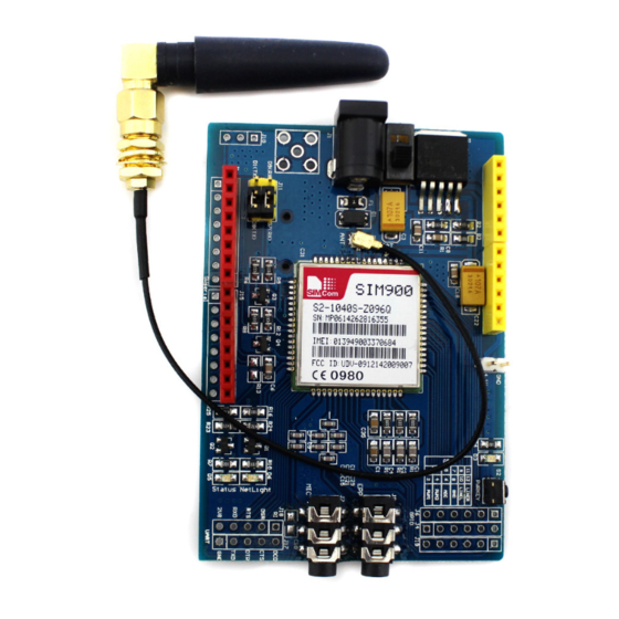
Page 16: Sim900 Evaluation Board
SIM900 Hardware Design 2.3 SIM900 Evaluation Board In order to help you on the application of SIM900, SIMCom can supply an Evaluation Board (EVB) that interfaces the SIM900 directly with appropriate power supply, SIM card holder, RS232 serial port, handset port, earphone port, line in port, antenna and all GPIO of the SIM900. -
Page 17: Application Interface
SIM900 Hardware Design 3 Application Interface SIM900 is equipped with a 68-pin SMT pad that connects to the cellular application platform. Sub-interfaces included in these SMT pads are described in detail in following chapters: Power supply (please refer to Chapter 3.3) Serial interfaces (please refer to Chapter 3.8) - Page 18 SIM900 Hardware Design VDD_EXT 2.8V output power supply Vmax=2.95V If unused, keep Vmin=2.70V open. Vnorm=2.80V Iout(max)= 10mA Ground Power on or power off PIN NAME DESCRIPTION DC CHARACTERISTICS PWRKEY Voltage input for PWRKEY. VILmax=0.15*VDD_EXT already PWRKEY should be pulled VIHmin=0.85* VDD_EXT pulled up.
- Page 19 SIM900 Hardware Design C bus clock If unused keep open C bus data KBR0~KBR4 If unused keep these pins open Keypad interface KBC0~KBC4 Pull VDD_EXT, unused keep pins open Serial port PIN NAME DESCRIPTION DC CHARACTERISTICS COMMENT Receive data VILmax=0.15 *VDD_EXT VIHmin=0.85*VDD_EXT...
-
Page 20: Operating Modes
SIM900 Hardware Design VOHmin= SIM_VDD-0.1V with VOLmax=0.1V diode array. VOHmax= SIM_VDD Maximum cable VOLmin= 0V length 200mm from the module pad to SIM card holder. SIM_PRESE SIM detect VILmax=0.15 *VDD_EXT If unused keep VIHmin=0.85*VDD_EXT open VILmin= 0V VIHmax= VDD_EXT PIN NAME... -
Page 21: Power Supply
3.3 Power Supply The power supply of SIM900 is from a single voltage source of VBAT= 3.1V...4.8V. In some case, the ripple in a transmitting burst may cause voltage drops when current consumption rises to typical peaks of 2A. So the power supply must be able to provide sufficient current up to 2A. -
Page 22: Figure 3: Reference Circuit Of The Vbat Input
2A peak current in burst mode of the module. The single 3.6V Li-Ion cell battery type can be connected to the power supply of the SIM900 VBAT directly. But the Ni_Cd or Ni_MH battery types must be used carefully, since their maximum voltage can rise over the absolute maximum voltage for the module and damage it. -
Page 23: Power Supply Pins
3.4 Power Up and Power Down Scenarios In general, be sure not to turn on SIM900 while it is beyond the safety limits of voltage and temperature stated in Chapter 3.4.2. SIM900 would immediately switch off after having started and detected these inappropriate conditions. -
Page 24: Figure 6: Turn On Sim900 Using Driving Circuit
However if the SIM900 is set autobauding, the serial port will receive nothing. The AT commands can be set after the SIM900 is power on. You can use AT+IPR=x to set a fixed baud rate and save the configuration to non-volatile flash memory. -
Page 25: Figure 8: Timing Of Turn On System Using Pwrkey
Undefined Figure 8: Timing of turn on system using PWRKEY When power on procedure completes, the SIM900 will send out following result code to indicate the module is ready to operate when set as fixed baud rate. This result code does not appear when autobauding is active. -
Page 26: Turn Off Sim900
3.4.2 Turn Off SIM900 Following ways can be used to turn off the SIM900: Normal power down procedure: Turn off SIM900 using the PWRKEY pin Normal power down procedure: Turn off SIM900 using AT command Over-voltage or under-voltage automatic shutdown: Take effect if over-voltage or under-voltage is detected... -
Page 27: Figure 12: Timing Of Turn Off System Using Pwrkey
3.4.2.1 Turn Off SIM900 Using the PWRKEY Pin (Power down) You can turn off the SIM900 by driving the PWRKEY to a low level voltage for a short time and then release. You also can urn off the SIM900 by connecting PWRKEY and PWRKEY_OUT for a short time and then release. - Page 28 SIM900 Hardware Design 3.4.2.2 Turn Off SIM900 Using AT Command You can use the AT command “AT+CPOWD=1” to turn off the module. This command lets the module log off from the network and allows the module to enter into a secure state and save data before completely disconnecting the power supply.
-
Page 29: Restart Sim900 Using The Pwrkey Pin
3.4.3 Restart SIM900 Using the PWRKEY Pin You can restart SIM900 by driving the PWRKEY to a low level voltage for a short time and then release, the same as turning on SIM900 using the PWRKEY pin. Before restarting the SIM900, you need delay at least 500ms from detecting the STATUS low level on. -
Page 30: Sleep Mode (Slow Clock Mode)
SIM900 Hardware Design card function will not be accessible. If SIM900 has been set by “AT+CFUN=4”, the RF function will be closed, the serial port is still active. In this case all AT commands correlative with RF function will not be accessible. -
Page 31: Rtc Backup
SIM900 Hardware Design 3.7 RTC Backup The RTC (Real Time Clock) power supply of module can be provided by an external capacitor or a battery (rechargeable or non-chargeable) through the VRTC. Note: If the RTC function is enabled, a battery or capacitor should be connected with the VRTC pin. If RTC Backup is not needed, please don’t keep it floating, a 4.7uF capacitor is recommended to connect to this pin. -
Page 32: Serial Interfaces
DBG_TXD Transmit data SIM900 provides two unbalanced asynchronous serial ports. One is the serial port and the other is the debug port. The GSM module is designed as a DCE (Data Communication Equipment), following the traditional DCE-DTE (Data Terminal Equipment) connection. The module and the client (DTE) are connected through the following signal (as following figure shows). -
Page 33: Function Of Serial Port & Debug Port Supporting
Serial port can be used for CSD FAX, GPRS service and send AT command of controlling module. Also serial port can be used for multiplexing function. SIM900 supports only basic mode of multiplexing so far. Serial port supports the communication rates as following: 1200, 2400, 4800, 9600, 19200, 38400, 57600 and 115200bps. -
Page 34: Software Upgrade And Software Debug
The TXD and RXD also should be connected to the IO connector, if user wants to send AT command or data stream to SIM900. The PWRKEY pin is recommended to connect to the IO connector. The user also can add a switch between the PWRKEY and the GND. -
Page 35: Audio Interfaces
SIM900 Hardware Design Figure 21: Connection of software upgrade and software debug The serial port and the debug port don’t support the RS_232 level and it only supports the CMOS level. Please refer to the table 10 for details about the voltage level. You should add the level converter IC between the DCE and DTE, if you connect it to the computer. -
Page 36: Speaker Interface Configuration
SIM900 Hardware Design It is suggested that you adopt one of the following two matching circuits in order to improve audio performance. The difference audio signals have to be layout according to difference signal layout rules. As show in following figures (Note: all components package are 0603.) If you want to adopt an amplifier circuit for audio, we... -
Page 37: Microphone Interfaces Configuration
SIM900 Hardware Design 3.9.2 Microphone Interfaces Configuration Close to Microphone Differential layout 10pF 33pF ANTI MIC_P Electret MODULE 10pF 33pF Microphone MIC_N 33pF 10pF ANTI Figure 25: Microphone interface configuration 3.9.3 Earphone Interface Configuration Close to Socket Close to MODULE... -
Page 38: Sim Card Interface
SIM900 Hardware Design Parameter Unit Working Voltage Working Current External Microphone Load Resistance k Ohms Internal biasing DC Characteristics Differential input <1% 15.9 mVrms voltage F=1KHz; pre-amp gain = 20 dB; PGA gain = 14 dB <5% mVrms F=1KHz;pre-amp gain = 0 dB; PGA... -
Page 39: Table 12: Pin Define Of The Sim Interface
SIM900 Hardware Design Both 1.8V and 3.0V SIM Cards are supported. The SIM interface is powered from an internal regulator in the module having normal voltage 3V. All pins reset as outputs driving low. Logic levels are as described in table... -
Page 40: Design Considerations For Sim Card Holder
SIM900 Hardware Design If you don’t use the SIM card detection function, you can leave the SIM_PRESENCE pin open. The reference circuit about 6 pins SIM card illustrates as following figure. 100nF CARD SIM_VDD SIM_RST SIM_CLK MODULE C707 10M006 512 2... -
Page 41: Table 14: Pin Description (Molex Sim Card Holder)
SIM900 Hardware Design Pin Name Signal Description SIM_VDD SIM Card Power supply, it can identify automatically the SIM Card power mode,one is 3.0V±10%, another is 1.8V±10%. Current is about 10mA. SIM_RST SIM Card Reset. SIM_CLK SIM Card Clock. Connect to GND. -
Page 42: Lcd Display Interface
SIM_PRESENCE Detect SIM Card Presence 3.11 LCD Display Interface SIM900 provides a serial LCD display interface that supports serial communication with LCD device. When used as LCD interface, the following table is the pin definition. LCD interface timing should be united with the LCD device. -
Page 43: Table 16: Pin Define Of The Keypad Interface
MODULE KBR0 KBR1 KBR2 KBR3 KBR4 Figure 31: Reference circuit of the keypad interface Note: This function is not supported in the default firmware. There must be customized firmware if you want. Please contact SIMCom for more details. SIM900_HD_V1.05 06.23.2010... -
Page 44: Adc
SIM900 Hardware Design 3.13 ADC SIM900 provides one auxiliary ADC (General purpose analog to digital converter.) as voltage input pin, which can be used to detect the values of some external items such as voltage, temperature etc. We can use AT command “AT+CADC”... -
Page 45: Network Status Indication
Hang on MO or Power on Ring Ring MO or MT Ring (talking) Hang up Hang up Figure 33: SIM900 Services as Receiver HIGH calling Echo Hang up Power on calling Echo talking Hang up Figure 34: SIM900 Services as caller 3.15 Network Status Indication... -
Page 46: General Purpose Input Output (Gpio)
3.16 General Purpose Input Output (GPIO) SIM900 provides a limited number of General Purpose Input/Output signal pin. The output and input voltage level of the GPIO can be set by AT command. For more details, please refer to document [1]... -
Page 47: External Reset
Note: This function is not supported in the default firmware. There must be customized firmware if you want. Please contact SIMCom for more details. 3.19 I2C Bus The SIM900 initiates a data transfer on the bus and generates the clock signal to execute the transfer. The features include the following: Maximum output rate equal to 400 kbit/s... -
Page 48: Antenna Interface
Please contact SIMCom for more details. 4 Antenna Interface SIM900 provides RF antenna interface. And customer’s antenna should be located in the customer’s main board and connect to module’s antenna pad through microstrip line or other type RF trace which impendence must be controlled in 50Ω. -
Page 49: Module Operating Frequencies
The operating temperature is listed in following table: Table 27 : SIM900 operating temperature Parameter Unit Ambient temperature ℃ Restricted operation* -40 to -30 +80 to +85 ℃ Storage temperature ℃ * The SIM900 does work, but deviations from the GSM specification may occur. SIM900_HD_V1.05 06.23.2010... -
Page 50: Power Supply Ratings
SIM900 Hardware Design 5.3 Power Supply Ratings Table 28 : SIM900 power supply ratings Parameter Description Conditions Unit VBAT Supply voltage Voltage must stay within the min/max values, including voltage drop, ripple, and spikes. Voltage drop Normal condition, power control level for... -
Page 51: Current Consumption(Vbat = 3.8V)
5.4 Current Consumption (VBAT = 3.8V) Please refer to the following table for the values of current consumption. Table 29 : SIM900 current consumption(VBAT = 3.8V) Voice Call GSM 850/EGSM 900 @power level #5 <300mA,Typical 250mA @power level #12,Typical 110mA... -
Page 52: Electro-Static Discharge
The GSM engine is not protected against Electrostatic Discharge (ESD) in general. Therefore, it is subject to ESD handing precautions that typically apply to ESD sensitive components. Proper ESD handing and packaging procedures must be applied throughout the processing, handing and operation of any application using a SIM900 module. -
Page 53: Figure 37: Top An Side Mechanical Dimensions Of Module (Unit: Mm
SIM900 Hardware Design Figure 37: Top an Side Mechanical dimensions of module (Unit: mm) SIM900_HD_V1.05 06.23.2010... -
Page 54: Figure 38:Bottom Mechanical Dimensions Of Module (Unit: Mm
SIM900 Hardware Design Figure 38:Bottom Mechanical dimensions of module (Unit: mm) Figure 39: Recommended PCB decal(Unit: mm) Note: Area A is keep route out area. Area B should be covered by silkscreen to prevent from the short between the via on customer board and the test points on the bottom side of the module. -
Page 55: Top And Bottom View Of The Sim900
SIM900 Hardware Design 6.2 Top and Bottom View of the SIM900 Figure 40: Top view of the SIM900 SIM900_HD_V1.05 06.23.2010... -
Page 56: Pin Assignment Of Sim900
TOP VIEW GPIO3/KBR2 DISP_CLK GPIO2/KBR3 DISP_DATA GPIO1/KBR4 DISP_D/C DISP_CS VDD_EXT NRESET PWM2 PWM1 Figure 41: SIM900 pin out diagram (Top View) Table 31 : PIN assignment Pin Number Pin Name Pin Number Pin Name PWRKEY PMW1 PWRKEY_OUT PWM2 GPIO1/KBR4 GPIO2/KBR3... - Page 57 SIM900 Hardware Design GPIO5/KBR0 DISP_CLK DISP_DATA DISP_D/C GPIO6/KBC4 DISP_CS GPIO7/KBC3 VDD_EXT GPIO8/KBC2 NRESET GPIO9/KBC1 GPIO10/KBC0 NETLIGHT MIC_P MIC_N SPK_P VBAT SPK_N VBAT LINEIN_R VBAT LINEIN_L VRTC RF_ANT DBG_TXD DBG_RXD SIM_VDD SIM_DATA SIM_CLK STATUS SIM_RST GPIO11 SIM_PRESENCE GPIO12 SIM900_HD_V1.05 06.23.2010...
-
Page 58: The Ramp-Soak-Spike Reflow Profile Of Sim900
SIM900 Hardware Design 6.4 The Ramp-Soak-Spike Reflow Profile of SIM900 Figure 42: The ramp-soak-spike reflow profile of SIM900 SIM900_HD_V1.05 06.23.2010... - Page 59 SIM900 Hardware Design Contact us: Shanghai SIMCom Wireless Solutions Ltd. Add: SIM Technology Building, No.633, Jinzhong Road, Changning District, Shanghai P.R. China 200335 Tel: +86 21 3235 3300 Fax: +86 21 3235 3301 URL: www.sim.com/wm SIM900_HD_V1.05 06.23.2010...
Need help?
Do you have a question about the SIM900 and is the answer not in the manual?
Questions and answers