Advertisement
Total solder points: 159
Difficulty level:
beginner 1
2
3
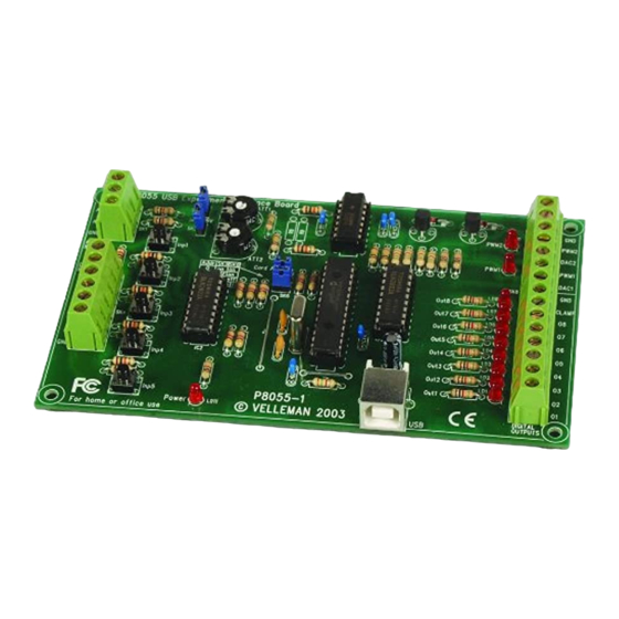
USB Experiment interface board
Specifications:
• 5 Digital inputs (0= ground, 1= open). On board test buttons pro-
vided.
• 2 Analog inputs with attenuation and amplification option. Internal
test +5V provided.
• 8 Digital open collector output switches (max 50V/100mA). On
board LED indication.
• 2 Analog outputs
0 to 5V, output resistance 1K5.
PWM 0 to 100% open collector outputs
max 100mA / 40V. On board LED indication.
• General conversion time: 20mS per command
• Power supply through USB approx. 70mA.
• Diagnostic software and communication DLL included
Minimum system:
• Pentium class CPU
• USB1.0 or higher connection
• Windows 98SE or higher (Win NT excluded)
• CD ROM player and Mouse
ILLUSTRATED ASSEMBLY MANUAL
4
5
advanced
K8055
H8055IP-1
Advertisement
Table of Contents

Related Manuals for Velleman K8055


Summary of Contents for Velleman K8055
- Page 1 Total solder points: 159 Difficulty level: beginner 1 advanced USB Experiment interface board K8055 Specifications: • 5 Digital inputs (0= ground, 1= open). On board test buttons pro- vided. • 2 Analog inputs with attenuation and amplification option. Internal test +5V provided.
- Page 2 (1) this device must not cause harm- ful interference and (2) the operation of this device should not be influenced by unwanted interference. More information about FCC can be look at http:// www.fcc.gov VELLEMAN Components NV Legen Heirweg 33 9890 Gavere Belgium Europe www.velleman.be...
- Page 3 Assembly hints 1. Assembly (Skipping this can lead to troubles ! ) Ok, so we have your attention. These hints will help you to make this project success- ful. Read them carefully. 1.1 Make sure you have the right tools: •...
- Page 4 Assembly hints 1.3 Soldering Hints : Mount the component against the PCB surface and carefully solder the leads Make sure the solder joints are cone-shaped and shiny Trim excess leads as close as possible to the solder joint AXIAL COMPONENTS ARE TAPED IN THE CORRECT MOUNTING SEQUENCE ! REMOVE THEM FROM THE TAPE ONE AT A TIME !
- Page 6 Construction R24 : 10K (1 - 0 - 3 - B) 1. Jumper R25 : 10K (1 - 0 - 3 - B) R26 : 10K (1 - 0 - 3 - B) R27 : 1K (1 - 0 - 2 - B) R28 : 47K (4 - 7 - 3 - B) R29 : 47K (4 - 7 - 3 - B) R30 : 47K (4 - 7 - 3 - B)
- Page 7 Construction 4. Capacitors 7. Potentiometer C... C1 : 100nF (104, 0.1, u1) RV1 : 100K C2 : 100nF (104, 0.1, u1) RV2 : 100K C3 : 100nF (104, 0.1, u1) C4 : 33pF (33) 8. Capacitors C5 : 33pF (33) C...
- Page 8 Construction 10. Transistors 14. Pin header T1 : BC337 T2 : BC337 SK2 : 2P 11. USB connector SK3 : 2P SK5 : 2P SK6 : 2P 15. Screw connectors SK7 : USBB90 12. Electrolytic capaci- tors. Check the polarity ! C...
-
Page 9: Gain Factor
Construction 16. IC’s. Watch the position of the notch! PIN 1 IC1 : TLV274IN IC2 : ULN2803 IC3 : VK8055 Programmed PIC16C745-IP ! SK8 : 5 x 3P IC4 : ULN2803 17. GAIN FACTOR When the input voltage is too low you can amplify it x4 / x15. A gain of x4 requires a resistance of 3K3 for R8 (input signal 1) and for R9 (input signal 2). - Page 10 Connections / settings 19. Connections / settings...
-
Page 11: Digital Outputs
Connections / settings 5 digital inputs (e.g. push button, switch, relay contact, ...). Input is generally "high" (1), connection to GND makes the input "low" (0) Analogue inputs (e.g. temperature sensor, potentiometer, ...) If the jumper is mounted, then you can use the internal voltage and adjust it using RV2/RV1. - Page 12 • Start “Setup.exe”, this software is located at the folder c:\..From the Velleman Software CD. If the necessary software is not included or if you want to check for updates, you can always download it for free from our Velleman Website www.velleman.be...
-
Page 13: Test Procedure
After startup LD4 (output 4) will flash momentarily to indicate that the circuit works as it should. Start the program 'K8055_Demo.exe'. Next press the 'connect' button to connect the K8055 with the computer. The message "Card x connected" is displayed if the connection is successful, see fig 3.0. - Page 14 Test procedure You can now simulate the inputs via push buttons Inp1 through Inp5. The matching check box remains ticked off as long as you keep one of the push buttons pressed down. Always tick off the check box for the matching output if you wish to test a digital output.
- Page 15 Schematic diagram 22. Schematic diagram.
-
Page 16: Pcb Layout
23. PCB layout. Modifications and typographical errors reserved © Velleman Components nv. H8055IP - 2003 - ED1...
Need help?
Do you have a question about the K8055 and is the answer not in the manual?
Questions and answers