Table of Contents
Advertisement
Quick Links
Advertisement
Table of Contents
Troubleshooting

Related Manuals for Hytera PD505


Summary of Contents for Hytera PD505
- Page 1 PORTABLE...
- Page 2 Preface This manual describes the information related to the product repair. It is intended for use by qualified technicians only. To repair the product properly, please read this manual carefully before repairing. This manual is applicable to the following product: PD50X Digital Portable Radio (X may represent 2, 5, 6 or 8)
- Page 3 Copyright Information Hytera is the trademark or registered trademark of Hytera Communications Co., Ltd. (the Company) in PRC and/or other countries or areas. The Company retains the ownership of its trademarks and product names. All other trademarks and/or product names that may be used in this manual are properties of their respective owners.
- Page 4 Documentation Information Conventions Instructional Conventions Icon Description Indicates information that can help you make better use of your product. Note Indicates references that can further describe the related topics. Caution Indicates situations that could cause data loss or equipment damage. Warning Indicates situations that could cause minor personal injury.
- Page 5 VHF (136-174 MHz)
-
Page 6: Table Of Contents
VHF (136-174 MHz) Contents Contents 1. Product Controls ..........................1 2. Disassembly and Assembly ........................ 2 3. Exploded View and Packaging Guide ....................5 3.1 Exploded View ..........................5 3.2 Packaging Guide ..........................7 4. Specifications ............................8 4.1 Specifications ............................ 8 5. -
Page 7: Product Controls
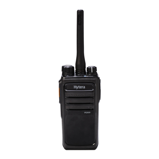
VHF (136-174 MHz) Product Controls 1. Product Controls Part Name Part Name PTT (Push-to-Talk) Key Accessory connector SK1 (Side Key 1) Microphone Channel Selector Knob Battery Latch Speaker Antenna LED Indicator Belt Clip Power On-Off/Volume Control Knob Battery... -
Page 8: Disassembly And Assembly
VHF (136-174 MHz) Disassembly and Assembly 2. Disassembly and Assembly This section is designed to introduce the way to disassemble the radio. To assemble the radio, do vice versa. Caution Please position the waterproof ring properly during reassembly. After reassembly, please check the waterproof performance of the radio using the waterproof test ... - Page 9 VHF (136-174 MHz) Disassembly and Assembly Step 4 Loosen the two screws on the bottom of the aluminum chassis. Step 5 Remove the aluminum chassis along with the main board. Step 6 Loosen the seven screws on the main board.
- Page 10 VHF (136-174 MHz) Disassembly and Assembly Step 7 Desolder the soldering joint of the antenna and remove the main board.
-
Page 11: Exploded View And Packaging Guide
VHF (136-174 MHz) Exploded View and Packaging Guide 3. Exploded View and Packaging Guide Exploded View Parts list: Part No. Description Qty. No. Part No. Description Qty. 6001978000000 Accessory connector cover 4400100036000 SMA RF connector 6001881100000 Front case 6001882000000 Rear cover PTT and programmable key 6100892100000 7103006004000... - Page 12 VHF (136-174 MHz) Exploded View and Packaging Guide Note Parts that are not marked with Part Number may vary with the frequency band.
-
Page 13: Packaging Guide
VHF (136-174 MHz) Exploded View and Packaging Guide Packaging Guide... -
Page 14: Specifications
VHF (136-174 MHz) Specifications 4. Specifications Specifications General Frequency Range 136 MHz-174 MHz Channel Capacity Channel Spacing 25 KHz/20 KHz/12.5 KHz Rated voltage: 7.4 V Operating Voltage Extreme voltage: 6.2–8.4 V Battery 1500 mAh Li-Ion battery Battery Life (5-5-90 Duty Cycle, High TX Power) Analog: 11 hours High-capacity 2000 mAh Li-Ion... - Page 15 VHF (136-174 MHz) Specifications Blocking 84 dB Rated Audio Power Output 0.5 W (16 Ω load) Rated Audio Distortion ≤3% Transmitter Power Output 5 W/1 W -36 dBm<1 GHz Conducted/Radiated Emission -30 dBm>1 GHz ±2.5 kHz@12.5 kHz Modulation Limiting ...
-
Page 16: Circuit Description
VHF (136-174 MHz) Circuit Description 5. Circuit Description Baseband Section 5.1.1 Power Supply Module Diagram of Power Control RF PA 7.4V RD07MUS2B AF PA 7.4V TDA2822D U 304 XC6204F502PR 3V3A_RX_RF 5VA_TX VCCcp _ main Charge pump supply 2.7V-5V VCCdigital : Digital supply , 2.7V-3V-3.3V U 306 VCCxtal : Crystal oscillator ECL / CML, 2.7V-3V-3.3V;... -
Page 17: Control Module
VHF (136-174 MHz) Circuit Description On-Off/Volume Control knob is on, SW- and SW+ are at high level, and the radio powers up. After power-on, Pwr_Hold goes to high level, and Pwr_Key_Det goes to low level. During power-off, SW- is at low level, while Pwr_Key_Det is at high level. The system detects power-off procedure via Pwr_Key_Det and implements the power-off procedure. - Page 18 VHF (136-174 MHz) Circuit Description...
- Page 19 VHF (136-174 MHz) Circuit Description RX-Unit TX DAC IF-RX TX、RX、 TLV5614 AD9864 SKY72310 CTRL GPIOs McBSP2 MCSI1 McBSP3 FLASH TMS320C55x GPIO Mobile SDRAM McBSP1 McBSP1 32MB JTAG TX OMAP5912 To AD9864 Audio Codec 19.2MHz BCLK To PLL MCLK TCXO TLV320AIC29 19.2MHz OMAP5912 BUZZ_IN...
- Page 20 VHF (136-174 MHz) Circuit Description SDRAM OMAP5912 FLASH SDRAM.A0: FLASH.A1: A0:A10 A1:A24 SDRAM.A13 FLASH.A24 SDRAM.D0: FLASH.D0: DQ0:DQ15 D0:D15 SDRAM.D15 FLASH.D15 RESET# SDRAM.CS# SDRAM.CS# RST_OUT# FLASH.OE# SDRAM.BA0 SDRAM.BA0 FLASH.WE# SDRAM.BA1 SDRAM.BA1 FLASH.WP# CAS# SDRAM.CAS# FLASH.RDY FLASH.RDY RAS# SDRAM.RAS# FLASH.CS3# LDQM SDRAM.DQML UDQM SDRAM.DQMU SDRAM.WE#...
- Page 21 VHF (136-174 MHz) Circuit Description Clock U1002 OMAP5912 ULPD_PLL_CLK CLK32K_IN OSC32K_OUT X1001 APLL 19.2MHz 96MHz OSC32K_IN 32.768KHz 20pF 20pF ULPD OMAP3.2 ARM_CK VSS(Y13) X8001 OSC1_OUT VCONT DPLL1 CK_REF DSP_CK OSC1_IN TCXO 19.2MHz TC_CK MCLK 19.2MHz MCLK U801 TLV320AIC29 Input Clock ...
- Page 22 VHF (136-174 MHz) Circuit Description SPIF.CS2(T19) AD9864 SPIF.SCK(U19) SPIF.DOUT(W21) SPIF.CS1 (U18) OMAP5912 MCBSP OMAP5912 provides 3 MCBSP interfaces: MCBSP1, MCBSP2 and MCBSP3. MCBSP1 is connected to the I S interface of the audio codec, to realize two-way transmission of digital voice and data. MCBSP2 uses independent clock and frame synchronization for transmission and reception.
- Page 23 VHF (136-174 MHz) Circuit Description data applying. U1002 OMAP5912 Cable USB_DN(R8) USB_DP(P9) OMAP5912 provides one I C interface, and supports a communication rate up to 400Kbps. OMAP5912 C is used for connecting to the acceleration sensor and works in the slave mode. The connection of I is shown below.
-
Page 24: Audio Module
VHF (136-174 MHz) Circuit Description MCSI1.SYNC(W8) SKY72310 MCSI1.CLK(M15) MCSI1.DOUT(W14) Data U1002 OMAP5912 5.1.3 Audio Module Audio Diagram The audio module is mainly for audio input and output. TLV320AIC29 is used as the audio codec to convert and process audio signal and digital signal. The audio amplifier TDA2822 is used to amplify the analog audio signal. -
Page 25: Rf Section
VHF (136-174 MHz) Circuit Description DSP for processing. Then the signal is sent to DAC (TLV5614), which converts the signal to modulation signal. After modulated and amplified in the RF module, the signal is sent out from the antenna. The RF signal received by the RF module is converted to digital signal by ADC (AD9864), and is then sent to DSP for demodulation and processing. -
Page 26: Receiver Circuit
VHF (136-174 MHz) Circuit Description Drive-stage Final-stage Pre-driver1 Gain:14dB Gain:10dB Po(max):29dBm Gain:18dB Po(max):38.5dBm Tx/Rx Switch Microstrip Po(-1dB):15.5dBm static I d:120mA static I PI MATCH d:200mA static Ic:25mA Matcher S21:-0.2dB ATT:-10dB S21: < - S21: < - 0.5dB 0.5dB Pi Attenuator S11:<... - Page 27 VHF (136-174 MHz) Circuit Description Tx/Rx Switch S21:-0.2dB TV/APC 4CH DAC TLV5614 S21:< -0.8dB BW(-3dB):570MHZ Stop band attenuation :-54dBc OSC level:> 4dBm Ref.Osc TV1 /APC 19.2MHz S21:12dB NF:< 3dB Stop band attenuation(-2&IF1st) :-80dBc IIP3:> 5dBm OMAP I/Q singal AD9864 Stop band filter Mixer Low-Noise Amp Band-pass Filter2...
- Page 28 VHF (136-174 MHz) Circuit Description Receiver Back-end The first IF signal (44.85 MHz) output by the IF amplifier goes into AD9864 (U6001) via Pin 47, where the signal is converted to the second IF signal (2.25 MHz). Then the signal is converted to digital signal via ADC sampling, and output via the SSI interface.
- Page 29 VHF (136-174 MHz) Circuit Description MOD1 VCO_L 341.95-400MHz RX/TX RX/TX VCO Buffer VCO Amplifier TV/APC VCO_H 400-411.95MHz TLV5614 400-470MHz 680MHz-1040MHz Frequency Synthesizer Ref.Osc MOD2+Freq error shift 19.2MHz From OMAP MCSI1/SPI(CS1) CV BUFFER Adapt CV OUT CV READ CTRL Adapt Control OMAP Operation Principle of PLL The 19.2MHz frequency generated by the reference crystal oscillator goes to PLL for division,...
-
Page 30: Troubleshooting Flow Chart
VHF (136-174 MHz) Troubleshooting Flow Chart 6. Troubleshooting Flow Chart Control Circuit Check the control circuit The product powers on The control circuit The RF circuit is normally?[1] is normal. normal?[2] Check U304, U306, U303 and control circuit. LED works normally? Replace LED 19.2MHz crystal Check U2013,... - Page 31 VHF (136-174 MHz) Troubleshooting Flow Chart [1] After the radio powers on, the LED indicator and alert tone works properly. [2] The RF power supply outputs normally, and the RX channel is on. [3] Output by the crystal oscillator: Vpp=700-800 mV, F=19.2 MHz.
- Page 32 VHF (136-174 MHz) Troubleshooting Flow Chart Receiver Circuit No Receive Check Q6004 3V3A_RX output is 3V3A_RX_RF output normal?[1] is normal?[2] The static working Check Q6005 point of Q6005 is normal?[3] The static working point Check Q6006, of Q6006/Q6007 is Q6007 normal?[4] Input IF signal via Check Q6003 and...
-
Page 33: Transmitter Circuit
VHF (136-174 MHz) Troubleshooting Flow Chart Description of Normal Situations: [1] Output voltage by Q6004 PIN3 is about 3.3 V. [2] Output voltage by U302 PIN5 or input voltage by Q6004 PIN4 is about 3.3 V. [3] Vgs: about 0.1 V; Vsd: about 3.3 V (in the case of no signal reception). [4] For Q6006, Vbe: about 0.76 V;... - Page 34 VHF (136-174 MHz) Troubleshooting Flow Chart No power output Check the power Power supply works supply circuit normally?[1] VGG is TV/APC Check DAC normal?[2] is normal?[3] output circuit Replace Q7009 and Q7010 TX_En 5VA_TX 3.3V is normal?[5] is normal?[5] TX_En 3.3V Check the power is normal?[4] supply circuit...
- Page 35 VHF (136-174 MHz) Troubleshooting Flow Chart [2] For low power, VGG: 1.8–2.1 V; for high power, VGG: 2.4–2.8 V. [3] For low power, TV/APC: 1-1.3 V; for high power, TV/APC: 1.8-2.1 V. [4] TX_En: about 3.3 V. [5] 5VA_TX: about 5 V. [6] High power: about 4.2 W;...
- Page 36 VHF (136-174 MHz) Troubleshooting Flow Chart FGU check Check the power The voltages of 5V_FGU, supply circuit 3V3A_RF and 3V3D_RF are normal? Q8002/Q8003 is Q8004/Q8008 is Replace VCO oscillates? normal?[1] normal?[2] Q8004/Q8008 Check Replace Q8004/Q8008 and Q8002/Q8003 peripheral components L8018/L8045 is Replace CV is normal?[3] normal?[4]...
- Page 37 VHF (136-174 MHz) Troubleshooting Flow Chart Q8003 PIN3: about 4 V. [2] During transmission, voltage at Q8008 E: about 1.8 V. During reception, voltage at Q8004 E: about 1.8 V. [3] The CV value varies with frequencies. Generally, it is within the range 0.5-4.5 V. [4] L8018/L8045 is on.
-
Page 38: Interface Definition
VHF (136-174 MHz) Interface Definition 7. Interface Definition J801 and J802: Double-Pin Interface for Earpiece, Programming and Downloading Pin No. Signal Function SPK- USB+ SPK+ J801 SPK+ SPK- J802 USB- OPTSEL1... -
Page 39: Tuning Description
VHF (136-174 MHz) Tuning Description 8. Tuning Description Required Test Instruments Radio test sets: Aeroflex 3920 and HP8921 3A/10V power supply Multimeter Tuner software Tuning Procedures 8.2.1 Tuning a Radio After the radio is reassembled, it must be tuned via the Tuner software. The specific operations are described in the table below. - Page 40 VHF (136-174 MHz) Tuning Description Click the “Save” button to save your settings. Connect the antenna connector of the radio with HP8921, and set HP8921 to TX test mode. Set the HP8921 parameters as follows: IF Filter: 230 kHz Filter1: <20 Hz HPF Filter2: <15 kHz LPF De-Emphasis: OFF Transmit-to-Deviation...
- Page 41 VHF (136-174 MHz) Tuning Description Click the “Transmit Off” button. Click the “Save” button to save your settings. Connect the antenna connector of the radio with HP8921, and set HP8921 to TX test mode. Transmit Oscillator Open the Tuner software, go to “TUNE_DATA -> TX” and double click Voltage “Transmit Oscillator Voltage”...
-
Page 42: Test A Radio
VHF (136-174 MHz) Tuning Description Connect the antenna connector of the radio with HP8921, and set HP8921 to RX test mode. Receive Oscillator Open the Tuner software, go to “TUNE_DATA -> RX” and double click Voltage “Receive Oscillator Voltage” from the navigation tree on the left. Click the “Save”... - Page 43 VHF (136-174 MHz) 9. PCB...
- Page 44 VHF (136-174 MHz)
-
Page 45: Block Diagram
VHF (136-174 MHz) Block Diagram 10. Block Diagram Radio General Diagram IF Processor Switch ADC9864 Baseband Power Supply CODE OMAP TLV320AIC29IRGZ SDRAM Flash... - Page 46 VHF (136-174 MHz) Block Diagram Block Diagram of FGU MOD1 VCO_L 341.95-400MHz RX/TX RX/TX VCO Buffer VCO Amplifier TV/APC VCO_H 400-411.95MHz TLV5614 400-470MHz 680MHz-1040MHz Frequency Synthesizer Ref.Osc MOD2+Freq error shift 19.2MHz From OMAP MCSI1/SPI(CS1) CV BUFFER Adapt CV OUT CV READ CTRL Adapt Control OMAP...
- Page 47 VHF (136-174 MHz) Block Diagram Drive-stage Final-stage Pre-driver1 Gain:14dB Gain:10dB Po(max):29dBm Tx/Rx Switch Gain:18dB Po(max):38.5dBm Microstrip Po(-1dB):15.5dBm static I d:120mA static I PI MATCH d:200mA static Ic:25mA Matcher S21:-0.2dB ATT:-10dB S21: < - S21: < - 0.5dB 0.5dB S11:< -15dB(140MHZ bandwidth) Pi Attenuator S21:<...
- Page 48 VHF (136-174 MHz) Block Diagram RF PA 7.4V RD07MUS2B AF PA 7.4V TDA2822D U304 XC6204F502PR 3V3A_RX_RF 5VA_TX VCCcp_main Charge pump supply 2.7V-5V VCCdigital:Digital supply,2.7V-3V-3.3V U306 VCCxtal : Crystal oscillator ECL/CML, 2.7V-3V-3.3V; 5VA_FGU XC6204F502PR VCCecl/cml: ECL/CML, 2.7V-3V-3.3V; PLL(SKY72310) DVDD 4.5V-5V-5.5V(5V Supply) 2.7V-3V-3.3V(3 Supply) No load,run clk:: Slow1.4mA/Fast 3.5mA(5V) Slow1mA/Fast 3mA(3V) AVDD 4.5V-5V-5.5V(5V Supply) 2.7V-3V-3.3V(3 Supply) DAC(TLV5604)
- Page 49 OMAP-CORE OMAP-CORE电路 SSP-T7-F SSP-T7-F X1001 X1001 C1002 NC C1002 NC OMAP_19.2M (11) C1001 C1001 C1003 C1003 20pF 20pF 20pF 20pF L1001 470nH L1001 470nH C1004 1000pF C1004 1000pF C1005 C1005 C1006 C1006 270pF 270pF 330pF 330pF 1V3D CVDD-1 CVDD-2 CVDD-3 CVDD-4 CVDD1 1V3D...
- Page 50 270pF C1086 C1086 270pF 270pF 270pF 270pF SPK- (10) Flash_D5 Flash_D4 SPK+ (10) 3V6D Flash_D3 3V3D Flash_D2 Flash_D1 Hytera Communications Co.Ltd. Hytera Communications Co.Ltd. Hytera Communications Co.Ltd. C1082 C1082 C1083 C1083 C1080 C1080 L103 L103 C1087 C1087 C1088 C1088 Flash_D0...
- Page 51 C1055 C1055 C1056 C1056 R1017 0 R1017 0 0.22uF 0.22uF 0.22uF 0.22uF Hytera Communications Co.Ltd. Hytera Communications Co.Ltd. Hytera Communications Co.Ltd. Model Name: Model Name: Model Name: DMR OMAP PD500 U1 DMR OMAP PD500 U1 DMR OMAP PD500 U1 Page:...
- Page 52 1.5k 1.5k USB.PUEN R1029 R1029 R1030 R1030 U1002B U1002B OMAP5912ZZG-1 OMAP5912ZZG-1 Hytera Communications Co.Ltd. Hytera Communications Co.Ltd. Hytera Communications Co.Ltd. Model Name: Model Name: Model Name: DMR OMAP PD500 U1 DMR OMAP PD500 U1 DMR OMAP PD500 U1 Page: Page:...
- Page 53 C139 NC/R3112Q271A NC/R3112Q271A C372 C372 U308 U308 0.22u 0.22u NC/R3112Q271A NC/R3112Q271A Hytera Communications Co.Ltd. Hytera Communications Co.Ltd. Hytera Communications Co.Ltd. Model Name: Model Name: Model Name: DMR OMAP PD500 U1 DMR OMAP PD500 U1 DMR OMAP PD500 U1 Page: Page:...
- Page 54 NTA7002N NTA7002N Acce_Sel1 R840 R840 R842 R842 C836 C836 0.1u 0.1u Hytera Communications Co.Ltd. Hytera Communications Co.Ltd. Hytera Communications Co.Ltd. Model Name: Model Name: Model Name: DMR OMAP PD500 U1 DMR OMAP PD500 U1 DMR OMAP PD500 U1 Page: Page:...
- Page 55 3300pF 3300pF 2.2pF 2.2pF HVC350B HVC350B C6051 C6051 0.68uF 0.68uF 18MHz采样时钟 Hytera Communications Co.Ltd. Hytera Communications Co.Ltd. Hytera Communications Co.Ltd. Model Name: Model Name: Model Name: DMR OMAP PD500 U1 DMR OMAP PD500 U1 DMR OMAP PD500 U1 Page: Page:...
- Page 56 82nH 82pF 82pF T6002 T6002 4BMH 4BMH D6009 D6009 HSMS-2827 HSMS-2827 Hytera Communications Co.Ltd. Hytera Communications Co.Ltd. Hytera Communications Co.Ltd. Model Name: Model Name: Model Name: DMR OMAP PD500 U1 DMR OMAP PD500 U1 DMR OMAP PD500 U1 Page: Page:...
- Page 57 R7048 R7048 R7014 R7014 R7049 R7049 (2,5) TX_En EM6M2 EM6M2 运放控制方案备用电源 Hytera Communications Co.Ltd. Hytera Communications Co.Ltd. Hytera Communications Co.Ltd. Model Name: Model Name: Model Name: DMR OMAP PD500 U1 DMR OMAP PD500 U1 DMR OMAP PD500 U1 Page: Page:...
- Page 58 R7052 470p 470p C7070 C7070 D7004 D7004 0.1uF 0.1uF NC/BA277 NC/BA277 Hytera Communications Co.Ltd. Hytera Communications Co.Ltd. Hytera Communications Co.Ltd. Model Name: Model Name: Model Name: DMR OMAP PD500 U1 DMR OMAP PD500 U1 DMR OMAP PD500 U1 Page: Page:...
- Page 59 100k 100k R8043 33 R8043 33 VCC_DAC_Ref10 DAC_MCBSP2_FSX C8061 C8061 47pF 47pF Hytera Communications Co.Ltd. Hytera Communications Co.Ltd. Hytera Communications Co.Ltd. Model Name: Model Name: Model Name: DMR OMAP PD500 U1 DMR OMAP PD500 U1 DMR OMAP PD500 U1 Page:...
- Page 60 18nH 18nH 频率范围:680-1040MHz L8053 L8053 C8139 C8139 C8141 C8141 390nH 390nH Hytera Communications Co.Ltd. Hytera Communications Co.Ltd. Hytera Communications Co.Ltd. Model Name: Model Name: Model Name: DMR OMAP PD500 U1 DMR OMAP PD500 U1 DMR OMAP PD500 U1 Page: Page:...
-
Page 61: Part List
VHF (136-174 MHz) Part List 12. Part List Print Print Part No. Description No. Ref No. Part No. Description Schottky barrier 6203391000000 Shielding mask D6009 T1E 3301250300000 diode Variable resistor 6203391000000 Shielding mask D7001 T4C 3305180300000 diode 6203392000010 Shielding mask D7002 T3C 3399030000010 PIN diode C1001... - Page 62 VHF (136-174 MHz) Part List Print Print Part No. Description No. Ref No. Part No. Description C1044 T2K 3101052710000 270pF L302 B1G 3221506181000 Ferrite bead C1045 T2K 3101052710000 270pF L303 B2H 3217099153000 15uH C1046 T2K 3101053310030 330pF L304 3217099153000 15uH C1047 T1K 3101052710000 270pF L305...
- Page 63 VHF (136-174 MHz) Part List Print Print Part No. Description No. Ref No. Part No. Description C315 3101051040060 0.1uF L7906 T4D 3233099470000 8TR C316 3101074750000 4.7uF L7907 T3E 3217112102020 1uH C317 3101051040060 0.1uF L7909 T4D 3231351630000 3TR C318 3101062250000 2.2uF L7910 T4C 3233099185900 4TR C319...
- Page 64 VHF (136-174 MHz) Part List Print Print Part No. Description No. Ref No. Part No. Description Compound C375 3101051040060 0.1uF Q103 B1A 3503040000000 MOSFET C376 3101052710000 270pF Q300 B2F 3599990000610 N-MOSFET C377 3101052710000 270pF Q301 B2E 3505990000040 P-MOSFET C378 3101051040060 0.1uF Q302 3599990000610 N-MOSFET Compound...
- Page 65 VHF (136-174 MHz) Part List Print Print Part No. Description No. Ref No. Part No. Description B2J 3001011010080 100Ω 212 C6037 B3H 3101011030050 0.01uF R1019 213 C6038 B2H 3101014710010 470pF R1020 B2J 3001011010080 100Ω 214 C6039 B2H 3101014710010 470pF R1021 B2J 3001011010080 100Ω...
- Page 66 VHF (136-174 MHz) Part List Print Print Part No. Description No. Ref No. Part No. Description T2A 3001050000000 0Ω 266 C6102 T3C 3101055600000 56pF R314 267 C6103 T2D 3101055600000 56pF R316 B2G 3001050000000 0Ω 268 C6104 T2D 3101055600000 56pF R317 T2B 3001050000000 0Ω...
- Page 67 VHF (136-174 MHz) Part List Print Print Part No. Description No. Ref No. Part No. Description T1D 3001050000000 0Ω 320 C8004 3101011020060 1000pF R6047 321 C8005 3101011020060 1000pF R636 T4F 3001050000000 0Ω 322 C8008 3101011040080 0.1uF R7002 B4F 3001054330000 43KΩ 323 C8009 3101011020060 1000pF R7003...
- Page 68 VHF (136-174 MHz) Part List Print Print Part No. Description No. Ref No. Part No. Description B4H 3001011030080 10KΩ 374 C8061 3101014700000 47pF R8010 375 C8063 3101011020060 1000pF R8011 B4J 3001051000000 10Ω 376 C8064 3101011040080 0.1uF R8012 3001051010040 100Ω 377 C8065 3101014710010 470pF R8013 B4J 3001051000000 10Ω...
- Page 69 VHF (136-174 MHz) Part List Print Print Part No. Description No. Ref No. Part No. Description 3001011040030 100KΩ 427 C8115 T4H 3101011040080 0.1uF R8060 428 C8116 B3G 3101014710010 470pF R8061 3001015630000 56KΩ 429 C8117 B2F 3101051200020 12pF R8062 3001012240000 220KΩ 430 C8118 B2F 3101051200020 12pF R8063 B3G 3001055690000 5.6Ω...
- Page 70 VHF (136-174 MHz) Part List Print Print Part No. Description No. Ref No. Part No. Description contact switch C835 3101051020010 1000pF SW103 T5C Transformer C836 3101051040060 0.1uF T6001 T1E 5406000000200 C837 3101051020010 1000pF T6002 Spring plate for C838 3101051040060 0.1uF TP803 B2C 6203354000000 antenna...
- Page 71 UHF1 (400–470 MHz)
- Page 72 UHF1 (400-470 MHz) Contents Contents 1. Product Controls ..........................1 2. Disassembly and Assembly ......................2 3. Exploded View and Packaging Guide ....................5 3.1 Exploded View ..........................5 3.2 Packaging Guide ..........................7 4. Specifications ............................. 8 4.1 Specifications ..........................8 5.
- Page 73 UHF1(400-470MHz) Product Controls 1. Product Controls Part Name Part Name PTT (Push-to-Talk) Key Accessory Connector SK1 (Side Key 1) Microphone Channel Selector Knob Battery Latch Speaker Antenna LED Indicator Belt Clip Power On-Off/Volume Control Knob Battery...
- Page 74 UHF1(400-470MHz) Disassembly and Assembly 2. Disassembly and Assembly This section is designed to introduce the way to disassemble the radio. To assemble the radio, do vice versa. Caution Please position the waterproof ring properly during reassembly. After reassembly, please check the waterproof performance of the radio using the waterproof test ...
- Page 75 UHF1(400-470MHz) Disassembly and Assembly Step 4 Loosen the two screws on the bottom of the aluminum chassis. Step 5 Remove the aluminum chassis along with the main board. Step 6 Loosen the seven screws on the main board.
- Page 76 UHF1(400-470MHz) Disassembly and Assembly Step 7 Desolder the soldering joint of the antenna and remove the main board.
- Page 77 UHF1(400-470MHz) Exploded View and Packaging Guide 3. Exploded View and Packaging Guide Exploded View Parts list: Part No. Description Qty. No. Part No. Description Qty. 6001978000000 Accessory connector cover 4400100036000 SMA RF connector 6001881100000 Front case 6001882000000 Rear cover PTT and programmable key 6100892100000 7103006004000 Machine screw...
- Page 78 UHF1(400-470MHz) Exploded View and Packaging Guide Note Parts that are not marked with Part Number may vary with the frequency band.
- Page 79 UHF1(400-470MHz) Exploded View and Packaging Guide Packaging Guide...
- Page 80 UHF1(400-470MHz) Specifications 4. Specifications Specifications General Frequency Range 400–470 MHz Channel Capacity Channel Spacing 25 KHz/20 KHz/12.5 KHz Rated voltage: 7.4 V Operating Voltage Extreme voltage: 6.2 V–8.4 V Battery 1500 mAh Li-Ion battery Battery Life (5-5-90 Duty Cycle, High TX Power) Analog: 11 hours High-capacity 2000 mAh Li-Ion...
- Page 81 UHF1(400-470MHz) Specifications Blocking 84 dB 0.5 W (16 Ω load) Rated Audio Power Output Rated Audio Distortion ≤3% Transmitter Power Output 4 W/1 W -36 dBm<1 GHz Conducted/Radiated Emission -30 dBm>1 GHz ±2.5 kHz@12.5 kHz Modulation Limiting ...
- Page 82 UHF1(400-470MHz) Circuit Description 5. Circuit Description Baseband Section 5.1.1 Power Supply Module Diagram of Power Control RF PA 7.4V RD07MUS2B AF PA 7.4V TDA2822D U 304 XC6204F502PR 3V3A_RX_RF 5VA_TX VCCcp _ main Charge pump supply 2.7V-5V VCCdigital : Digital supply , 2.7V-3V-3.3V U 306 VCCxtal : Crystal oscillator ECL / CML, 2.7V-3V-3.3V;...
- Page 83 UHF1(400-470MHz) Circuit Description On-Off/Volume Control knob is on, SW- and SW+ are at high level, and the radio powers up. After power-on, Pwr_Hold goes to high level, and Pwr_Key_Det goes to low level. During power-off, SW- is at low level, while Pwr_Key_Det is at high level. The system detects power-off procedure via Pwr_Key_Det and implements the power-off procedure.
- Page 84 UHF1(400-470MHz) Circuit Description...
- Page 85 UHF1(400-470MHz) Circuit Description RX-Unit TX DAC IF-RX TX、RX、 TLV5614 AD9864 SKY72310 CTRL GPIOs McBSP2 MCSI1 McBSP3 FLASH TMS320C55x GPIO Mobile SDRAM McBSP1 McBSP1 32MB JTAG TX OMAP5912 To AD9864 Audio Codec 19.2MHz BCLK To PLL MCLK TCXO TLV320AIC29 19.2MHz OMAP5912 BUZZ_IN PWM0/PWT 32.768KHz...
- Page 86 UHF1(400-470MHz) Circuit Description SDRAM OMAP5912 FLASH SDRAM.A0: FLASH.A1: A0:A10 A1:A24 SDRAM.A13 FLASH.A24 SDRAM.D0: FLASH.D0: DQ0:DQ15 D0:D15 SDRAM.D15 FLASH.D15 RESET# SDRAM.CS# SDRAM.CS# RST_OUT# FLASH.OE# SDRAM.BA0 SDRAM.BA0 FLASH.WE# SDRAM.BA1 SDRAM.BA1 FLASH.WP# CAS# SDRAM.CAS# FLASH.RDY FLASH.RDY RAS# SDRAM.RAS# FLASH.CS3# LDQM SDRAM.DQML UDQM SDRAM.DQMU SDRAM.WE# SDRAM.CLK SDRAM.CKE...
- Page 87 UHF1(400-470MHz) Circuit Description Clock U1002 OMAP5912 ULPD_PLL_CLK CLK32K_IN OSC32K_OUT X1001 APLL 19.2MHz 96MHz OSC32K_IN 32.768KHz 20pF 20pF ULPD OMAP3.2 ARM_CK VSS(Y13) X8001 OSC1_OUT VCONT DPLL1 CK_REF DSP_CK OSC1_IN TCXO 19.2MHz TC_CK MCLK 19.2MHz MCLK U801 TLV320AIC29 Input Clock 32K Clock: It is also called “sleep clock” and is mainly used for system timing and sleeping. ...
- Page 88 UHF1(400-470MHz) Circuit Description SPIF.CS2(T19) AD9864 SPIF.SCK(U19) SPIF.DOUT(W21) SPIF.CS1 (U18) OMAP5912 MCBSP OMAP5912 provides 3 MCBSP interfaces: MCBSP1, MCBSP2 and MCBSP3. MCBSP1 is connected to the I S interface of the audio codec, to realize two-way transmission of digital voice and data. MCBSP2 uses independent clock and frame synchronization for transmission and reception.
- Page 89 UHF1(400-470MHz) Circuit Description data applying. U1002 OMAP5912 Cable USB_DN(R8) USB_DP(P9) OMAP5912 provides one I C interface, and supports a communication rate up to 400 Kbps. OMAP5912 C interface is used for connecting with the the acceleration sensor and works in the slave mode. The connection of I C is shown below.
- Page 90 UHF1(400-470MHz) Circuit Description MCSI1.SYNC(W8) SKY72310 MCSI1.CLK(M15) MCSI1.DOUT(W14) Data U1002 OMAP5912 5.1.3 Audio Module Audio Diagram The audio module is mainly for audio input and output. TLV320AIC29 is used as the audio codec to convert and process audio signal and digital signal. The audio amplifier TDA2822 is used to amplify the analog audio signal.
- Page 91 UHF1(400-470MHz) Circuit Description DSP for processing. Then the signal is sent to DAC (TLV5614), which converts the signal to modulation signal. After modulated and amplified in the RF module, the signal is sent out from the antenna. The RF signal received by the RF module is converted to digital signal by ADC (AD9864), and is then sent to DSP for demodulation and processing.
- Page 92 UHF1(400-470MHz) Circuit Description Drive-stage Final-stage Pre-driver1 Gain:14dB Gain:10dB Po(max):29dBm Tx/Rx Switch Gain:18dB Po(max):38.5dBm Microstrip Po(-1dB):15.5dBm static I d:120mA static I PI MATCH d:200mA static Ic:25mA Matcher S21:-0.2dB ATT:-10dB S21: < - S21: < - 0.5dB 0.5dB Pi Attenuator S11:< -15dB(140MHZ bandwidth) S21:<...
- Page 93 UHF1(400-470MHz) Circuit Description 5.2.2 Receiver Circuit The receiver circuit mainly comprises the RF band-pass filter, low-noise amplifier, mixer, IF filter, IF amplifier and IF processor. Tx/Rx Switch S21:-0.2dB TV/APC 4CH DAC TLV5614 S21:< -0.8dB BW(-3dB):570MHZ Stop band attenuation :-54dBc OSC level:> 4dBm Ref.Osc TV1 /APC 19.2MHz...
- Page 94 UHF1(400-470MHz) Circuit Description Receiver Back-end The first IF signal (58.05 MHz) output by the IF amplifier goes into AD9864 (U6001) via Pin 47, where the signal is converted to the second IF signal (2.25 MHz). Then the second IF signal is converted to digital signal via ADC sampling, and output via the SSI interface.
- Page 95 UHF1(400-470MHz) Circuit Description MOD1 VCO_L 341.95-400MHz RX/TX RX/TX VCO Buffer VCO Amplifier TV/APC VCO_H 400-411.95MHz TLV5614 400-470MHz 680MHz-1040MHz Frequency Synthesizer Ref.Osc MOD2+Freq error shift 19.2MHz From OMAP MCSI1/SPI(CS1) CV BUFFER Adapt CV OUT CV READ CTRL Adapt Control OMAP Operation Principle of PLL The 19.2 MHz frequency generated by the reference crystal oscillator goes to PLL for division, generating the reference frequency (i.e.
- Page 96 UHF1(400-470MHz) Troubleshooting Flow Chart 6. Troubleshooting Flow Chart Control Circuit Check the control circuit The product The control circuit powers on The RF circuit is is normal. normally?[1] normal?[2] Check U304 , U306 , U303 and control circuit Led works normally? Replace LED 19.2MHz crystal 3V3D is...
- Page 97 UHF1(400-470MHz) Troubleshooting Flow Chart [2] The RF power supply outputs normally, and the RX channel is on. [3] Output by the crystal oscillator: Vpp=700-800 mV, F=19.2 MHz.
- Page 98 UHF1(400-470MHz) Troubleshooting Flow Chart Receiver Circuit No Recieve 3V3A_RX output is 3V3A_RX_RF output Check Q6004 normal?[1] is normal?[2] The static working Check Q6005 point of Q6005 is normal?[3] The static working Check Q6006, point of Q6006/Q6007 Q6007 is normal?[4] Input IF signal via U6001PIN47 to check Check Q6003 and Second LO is normal?[6]...
- Page 99 UHF1(400-470MHz) Troubleshooting Flow Chart [2] Output voltage by U302 PIN5 or input voltage by Q6004 PIN4 is about 3.3 V. [3] Vgs: about 0.1 V; Vsd: about 3.3 V (in the case of no signal reception). [4] For Q6006, Vbe: about 0.76 V; Vce: about 0.95 V; for Q6007, Vbe: about 0.7 V; Vce: 0.85 V (in the case of no signal reception).
- Page 100 UHF1(400-470MHz) Troubleshooting Flow Chart No power output Check the Power supply works power supply normally?[1] circuit.. VGG is TV/APC is Check the DAC normal?[2] normal?[3] output circuit. Replace Q7009 and Q7010 5VA_TX is TX_En is normal?[5] normal?[5] TX_En 3.3V is Check the power normal?[4] supply circuit.
- Page 101 UHF1(400-470MHz) Troubleshooting Flow Chart Description of Normal Situations: [1] Voltage of the power supply: about 7.4 V. [2] For low power, VGG: 1.8–2.1 V; for high power, VGG: 2.4–2.8 V. [3] For low power, TV/APC: 1-1.3 V; for high power, TV/APC: 1.8-2.1 V. [4] TX_En: about 3.3 V.
- Page 102 UHF1(400-470MHz) Troubleshooting Flow Chart FGU check 5V_FGU, 3V3A_RF and Check the power supply 3V3D_RF are normal? circuit.. Q8004/Q8008 are Q8002/Q8003 are Replace Q8004 VCO oscillator? normal?[2] normal?[1] and Q8008. Check Q8004, Q8008 Replace Q8002 and and peripheral Q8003. components. Q 106 、Q 110 L8018 and L8045 Replace L8018 and CV is normal?[3]...
- Page 103 UHF1(400-470MHz) Troubleshooting Flow Chart Description of Normal Situations: [1] During transmission, output voltage by Q8002 PIN3: about 4 V. During reception, output voltage by Q8003 PIN3: about 4 V. [2] During transmission, voltage at Q8008 E: about 1.8 V. During reception, voltage at Q8004 E: about 1.8 V.
- Page 104 UHF1(400-470MHz) Interface Definition 7. Interface Definition Double-Pin Interface for Earpiece, Programming and Downloading Pin No. Signal Function SPK- USB+ SPK+ J801 SPK+ SPK- J802 USB- OPTSEL1...
- Page 105 UHF1(400-470MHz) Tuning Description 8. Tuning Description Required Test Instruments Radio communication test sets: Aeroflex 3920 and HP8921 3A/10V power supply Multimeter Tuner software Tuning Procedures 8.2.1 Tuning a Radio After the radio is reassembled, it must be tuned via the Tuner software. The specific operations are described in the table below.
- Page 106 UHF1(400-470MHz) Tuning Description Click the “Save” button to save your settings. Connect the antenna connector of the radio with the HP8921, and set the HP8921 to TX test mode. Set the HP8921 parameters as follows: IF Filter: 230 kHz Filter 1: <20 Hz HPF Filter 2: <15 kHz LPF De-Emphasis: OFF Open the Tuner software, go to “TUNER_DATA ->...
- Page 107 UHF1(400-470MHz) Tuning Description Keep the radio in a vertical position. Open the Tuner software, go to “TUNE_DATA -> RX” and double click Mandown Calibration “Mandown Calibration” from the navigation tree on the left. Click the “Read” button to read the calibration data. Click the “Save”...
- Page 108 UHF1(400-470MHz) 9. PCB...
- Page 109 UHF1(400-470MHz)
- Page 110 UHF1(400-470MHz) Block Diagram 10. Block Diagram Radio General Diagram IF Processor Switch ADC9864 Baseband Power Supply CODE OMAP TLV320AIC29IRGZ SDRAM Flash...
- Page 111 UHF1(400-470MHz) Block Diagram Diagram of FGU MOD1 VCO_L 341.95-400MHz RX/TX RX/TX VCO Buffer VCO Amplifier TV/APC VCO_H 400-411.95MHz TLV5614 400-470MHz 680MHz-1040MHz Frequency Synthesizer Ref.Osc MOD2+Freq error shift 19.2MHz From OMAP MCSI1/SPI(CS1) CV BUFFER Adapt CV OUT CV READ CTRL Adapt Control OMAP Block Diagram of RX Unit...
- Page 112 UHF1(400-470MHz) Block Diagram Drive-stage Final-stage Pre-driver1 Gain:14dB Gain:10dB Po(max):29dBm Tx/Rx Switch Gain:18dB Po(max):38.5dBm Microstrip Po(-1dB):15.5dBm static I d:120mA static I PI MATCH d:200mA static Ic:25mA Matcher S21:-0.2dB ATT:-10dB S21: < - S21: < - 0.5dB 0.5dB S11:< -15dB(140MHZ bandwidth) Pi Attenuator S21:<...
- Page 113 UHF1(400-470MHz) Block Diagram RF PA 7.4V RD07MUS2B AF PA 7.4V TDA2822D U304 XC6204F502PR 3V3A_RX_RF 5VA_TX VCCcp_main Charge pump supply 2.7V-5V VCCdigital:Digital supply,2.7V-3V-3.3V U306 VCCxtal : Crystal oscillator ECL/CML, 2.7V-3V-3.3V; 5VA_FGU XC6204F502PR VCCecl/cml: ECL/CML, 2.7V-3V-3.3V; PLL(SKY72310) DVDD 4.5V-5V-5.5V(5V Supply) 2.7V-3V-3.3V(3 Supply) No load,run clk:: Slow1.4mA/Fast 3.5mA(5V) Slow1mA/Fast 3mA(3V) AVDD 4.5V-5V-5.5V(5V Supply) 2.7V-3V-3.3V(3 Supply) DAC(TLV5604)
- Page 114 OMAP-CORE OMAP-CORE电路 SSP-T7-F SSP-T7-F X1001 X1001 C1002 NC C1002 NC OMAP_19.2M (11) C1001 C1001 C1003 C1003 20pF 20pF 20pF 20pF L1001 470nH L1001 470nH C1004 1000pF C1004 1000pF C1005 C1005 C1006 C1006 270pF 270pF 330pF 330pF 1V3D CVDD-1 CVDD-2 CVDD-3 CVDD-4 CVDD1 1V3D...
- Page 115 270pF C1086 C1086 270pF 270pF 270pF 270pF SPK- (10) Flash_D5 Flash_D4 SPK+ (10) 3V6D Flash_D3 3V3D Flash_D2 Flash_D1 Hytera Communications Co.Ltd. Hytera Communications Co.Ltd. Hytera Communications Co.Ltd. C1082 C1082 C1083 C1083 C1080 C1080 L103 L103 C1087 C1087 C1088 C1088 Flash_D0...
- Page 116 C1055 C1055 C1056 C1056 R1017 0 R1017 0 0.22uF 0.22uF 0.22uF 0.22uF Hytera Communications Co.Ltd. Hytera Communications Co.Ltd. Hytera Communications Co.Ltd. Model Name: Model Name: Model Name: DMR OMAP PD500 U1 DMR OMAP PD500 U1 DMR OMAP PD500 U1 Page:...
- Page 117 1.5k 1.5k USB.PUEN R1029 R1029 R1030 R1030 U1002B U1002B OMAP5912ZZG-1 OMAP5912ZZG-1 Hytera Communications Co.Ltd. Hytera Communications Co.Ltd. Hytera Communications Co.Ltd. Model Name: Model Name: Model Name: DMR OMAP PD500 U1 DMR OMAP PD500 U1 DMR OMAP PD500 U1 Page: Page:...
- Page 118 C139 NC/R3112Q271A NC/R3112Q271A C372 C372 U308 U308 0.22u 0.22u NC/R3112Q271A NC/R3112Q271A Hytera Communications Co.Ltd. Hytera Communications Co.Ltd. Hytera Communications Co.Ltd. Model Name: Model Name: Model Name: DMR OMAP PD500 U1 DMR OMAP PD500 U1 DMR OMAP PD500 U1 Page: Page:...
- Page 119 NTA7002N NTA7002N Acce_Sel1 R840 R840 R842 R842 C836 C836 0.1u 0.1u Hytera Communications Co.Ltd. Hytera Communications Co.Ltd. Hytera Communications Co.Ltd. Model Name: Model Name: Model Name: DMR OMAP PD500 U1 DMR OMAP PD500 U1 DMR OMAP PD500 U1 Page: Page:...
- Page 120 3300pF 3300pF 2.2pF 2.2pF HVC350B HVC350B C6051 C6051 0.68uF 0.68uF 18MHz采样时钟 Hytera Communications Co.Ltd. Hytera Communications Co.Ltd. Hytera Communications Co.Ltd. Model Name: Model Name: Model Name: DMR OMAP PD500 U1 DMR OMAP PD500 U1 DMR OMAP PD500 U1 Page: Page:...
- Page 121 82nH 82pF 82pF T6002 T6002 4BMH 4BMH D6009 D6009 HSMS-2827 HSMS-2827 Hytera Communications Co.Ltd. Hytera Communications Co.Ltd. Hytera Communications Co.Ltd. Model Name: Model Name: Model Name: DMR OMAP PD500 U1 DMR OMAP PD500 U1 DMR OMAP PD500 U1 Page: Page:...
- Page 122 R7048 R7048 R7014 R7014 R7049 R7049 (2,5) TX_En EM6M2 EM6M2 运放控制方案备用电源 Hytera Communications Co.Ltd. Hytera Communications Co.Ltd. Hytera Communications Co.Ltd. Model Name: Model Name: Model Name: DMR OMAP PD500 U1 DMR OMAP PD500 U1 DMR OMAP PD500 U1 Page: Page:...
- Page 123 R7052 470p 470p C7070 C7070 D7004 D7004 0.1uF 0.1uF NC/BA277 NC/BA277 Hytera Communications Co.Ltd. Hytera Communications Co.Ltd. Hytera Communications Co.Ltd. Model Name: Model Name: Model Name: DMR OMAP PD500 U1 DMR OMAP PD500 U1 DMR OMAP PD500 U1 Page: Page:...
- Page 124 100k 100k R8043 33 R8043 33 VCC_DAC_Ref10 DAC_MCBSP2_FSX C8061 C8061 47pF 47pF Hytera Communications Co.Ltd. Hytera Communications Co.Ltd. Hytera Communications Co.Ltd. Model Name: Model Name: Model Name: DMR OMAP PD500 U1 DMR OMAP PD500 U1 DMR OMAP PD500 U1 Page:...
- Page 125 18nH 18nH 频率范围:680-1040MHz L8053 L8053 C8139 C8139 C8141 C8141 390nH 390nH Hytera Communications Co.Ltd. Hytera Communications Co.Ltd. Hytera Communications Co.Ltd. Model Name: Model Name: Model Name: DMR OMAP PD500 U1 DMR OMAP PD500 U1 DMR OMAP PD500 U1 Page: Page:...
-
Page 126: Parts List
UHF1(400-470MHz) Parts List 12. Parts List Print Print Part No. Description Part No. Description Schottky barrier 6203391000000 Shielding cover 503 D6003 3303030300000 diode 6203391000000 Shielding cover 504 D6004 3304010100220 Varactor 6203392000010 Shielding cover 505 D6005 3304010100220 Varactor C1001 3101012000000 20PF 506 D6007 3304010100220 Varactor C1003... - Page 127 UHF1(400-470MHz) Parts List Print Print Part No. Description Part No. Description C1045 3101052710000 270PF 548 L1005 3221505121010 Ferrite bead C1046 3101053310030 330PF L103 3221505121010 Ferrite bead C1047 3101052710000 270PF L301 3221506181000 Ferrite bead C1048 3101052710000 270PF L302 3221506181000 Ferrite bead C1049 3101051040060 0.1UF L303...
- Page 128 UHF1(400-470MHz) Parts List Print Print Part No. Description Part No. Description C317 3101051040060 0.1UF 608 L7907 3213212561000 0.56uH C318 3101062250000 2.2UF 609 L7908 3233099449000 4.4nH C319 3101052240010 0.22UF 610 L8001 3221505121010 Ferrite bead C320 3101052710000 270PF 611 L8002 3221505121010 Ferrite bead C321 3101051040060 0.1UF 612 L8003...
- Page 129 UHF1(400-470MHz) Parts List Print Print Part No. Description Part No. Description N-MOSFET C376 3101052710000 270PF Q300 3599990000610 NTA7002NT1G P-MOSFET C377 3101052710000 270PF Q301 3505990000040 SI2343CDS N-MOSFET C378 3101051040060 0.1UF Q302 3599990000610 NTA7002NT1G Compound C379 3101074750000 4.7UF 669 Q6001 3403999000070 transistor 2SC3356-T1B-A- C380 3101054710010 470PF...
- Page 130 UHF1(400-470MHz) Parts List Print Print Part No. Description Part No. Description 208 C6034 B5H 3101012220000 2200pF 708 R1015 3001011030080 10KΩ 209 C6035 B4H 3101014710010 470PF 709 R1017 3001050000000 0Ω 210 C6036 B5H 3101011040080 0.1uF 710 R1018 3001011030080 10KΩ 211 C6037 B5H 3101011030050 0.01uF 711 R1019 3001011010080 100Ω...
- Page 131 UHF1(400-470MHz) Parts List Print Print Part No. Description Part No. Description 261 C6095 T2G 3101051800010 18PF R309 3001051540000 150KΩ 262 C6096 T3H 3101051500020 15PF R312 3001052720010 2.7KΩ 263 C6097 T2G 3101057590000 7.5PF R313 3001054740010 470KΩ 264 C6099 3101058200000 82PF R314 3001050000000 0Ω...
- Page 132 UHF1(400-470MHz) Parts List Print Print Part No. Description Part No. Description 314 C7068 3101054710010 470PF 814 R6042 3001011040030 100KΩ 315 C7069 3101054710010 470PF 815 R6043 3001015630000 56KΩ 316 C7071 3101061300000 13PF 816 R6046 3001058210000 820Ω 317 C8001 3101011040080 0.1uF 817 R6047 3001055690000 5.6Ω...
- Page 133 UHF1(400-470MHz) Parts List Print Print Part No. Description Part No. Description C806 3101051050160 1uF 868 R8009 3001011040030 100KΩ 369 C8060 3101011050000 1uF 869 R8010 3001011030080 10KΩ 370 C8061 3101014700000 47PF 870 R8011 3001011000050 10Ω 371 C8063 3101014710010 470PF 871 R8012 3001051010040 100Ω...
- Page 134 UHF1(400-470MHz) Parts List Print Print Part No. Description Part No. Description 422 C8113 3101053300000 33PF 922 R8060 3001011040030 100KΩ 423 C8114 T5H 3101014710010 470PF 923 R8061 3001015630000 56KΩ 424 C8115 T5H 3101011040080 0.1uF 924 R8062 3001011840000 180KΩ 425 C8116 3101014710010 470PF 925 R8063 3001055690000 5.6Ω...
- Page 135 UHF1(400-470MHz) Parts List Print Print Part No. Description Part No. Description BT antenna spring C833 3101051020010 1000PF 974 TP803 6203354000000 plate antenna C834 3101054710010 470PF 975 TP804 6203354000000 spring plate C835 3101051020010 1000PF 976 U1001 3612024000020 Memory C836 3101051040060 0.1UF 977 U1002 3610010000010 MCU C837...
- Page 136 1616300000260 2014-03-17 L07157...
Need help?
Do you have a question about the PD505 and is the answer not in the manual?
Questions and answers