Table of Contents
Advertisement
Advertisement
Table of Contents

Related Manuals for Terasic DE10-Lite


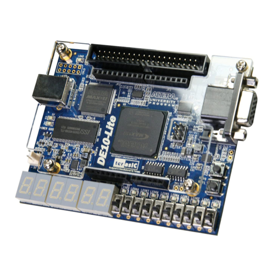
Summary of Contents for Terasic DE10-Lite
- Page 1 DE10-Lite www.terasic.com May 11, 2018 User Manual...
-
Page 2: Table Of Contents
2. 5 Accelerometer ..........................14 2. 6 VGA .............................. 15 2. 7 Overall Structure of the DE10-Lite Control Panel ................ 16 Chapter 3 Using the Starter Kit ................... 17 3. 1 Configuration of MAX 10 FPGA on DE10-Lite ................17 3. - Page 3 4. 3 Using DE10-Lite System Builder ....................43 Chapter 5 Examples of Advanced Demonstrations ............ 48 5. 1 DE10-Lite Factory Configuration ....................48 5. 2 SDRAM Test in Nios II ......................... 50 5. 3 SDRAM Test in Verilog ........................ 53 5.
-
Page 4: Chapter 1 Introduction
Chapter 1 Introduction The DE10-Lite presents a robust hardware design platform built around the Altera MAX 10 FPGA. The MAX 10 FPGA is well equipped to provide cost effective, single-chip solutions in control plane or data path applications and industry-leading programmable logic for ultimate design flexibility. -
Page 5: De10-Lite System Cd
• The DE10-Lite board • Type A Male to Type B Male USB Cable The DE10-Lite System CD contains the documentation and supporting materials, including the User Manual, Control Panel, System Builder, reference designs and device datasheets. User can download this System CD from the web (http://DE10-Lite.terasic.com/cd). - Page 6 • 1,638 Kbits M9K Memory • 5,888 Kbits user flash memory • 144 18 × 18 Multiplier • 4 PLLs • On-Board USB Blaster (Normal type B USB connector) • 64MB SDRAM, x16 bits data bus DE10-Lite www.terasic.com May 11, 2018 User Manual...
-
Page 7: Block Diagram Of The Board
To provide maximum flexibility for the user, all connections are made through the MAX 10 FPGA device. Thus, the user can configure the FPGA to implement any system design. Figure 1-4 Board Block Diagram DE10-Lite www.terasic.com May 11, 2018 User Manual... -
Page 8: Getting Help
Here are the addresses where you can get help if you encounter any problem: • Terasic Inc. 9F., No.176, Sec.2, Gongdao 5th Rd, East Dist, Hsinchu City, 30070. Taiwan Email: support@terasic.com Tel.: +886-3-5750-880 Web: http://DE10-Lite.terasic.com DE10-Lite www.terasic.com May 11, 2018... -
Page 9: Chapter 2 Control Panel
The Control Panel Software Utility is located in the directory “Tools/ControlPanel” in the DE10-Lite System CD. It's free of installation, just copy the whole folder to your host computer and launch the control panel by executing the “DE10_Lite_ControlPanel.exe”. - Page 10 LEDs and observing the result on the DE10-Lite board. Figure 2-1 The DE10-Lite Control Panel The “Control Circuit” that The concept of the DE10-Lite Control Panel is illustrated in Figure 2-2. performs the control functions is implemented in the FPGA board. It communicates with the Control Panel window, which is active on the host computer, via the USB Blaster link.
-
Page 11: Controlling The Leds, 7-Segment Displays
Figure 2-2 The DE10-Lite Control Panel concept The DE10-Lite Control Panel can be used to light up LEDs, change the values displayed on the 7-segment, monitor buttons/switches status, read/write the SDRAM Memory, output VGA color pattern to VGA monitor. The feature of reading/writing a word or an entire file from/to the Memory allows the user to develop multimedia applications without worrying about how to build a Memory Programmer. - Page 12 Figure 2-4. From the window, directly use the left-right arrows to control the 7-SEG patterns on the DE10-Lite board which are updated immediately. Note that the dots of the 7-SEGs are not enabled on the DE10-Lite board. Figure 2-4 Controlling 7-SEG display DE10-Lite www.terasic.com...
-
Page 13: Switches And Push-Buttons
Thus, it can be used for troubleshooting purposes. The Control Panel can be used to write/read data to/from the SDRAM chips on the DE10-Lite board. As shown below, we will describe how the SDRAM may be accessed; Click on the Memory tab and select “SDRAM”... - Page 14 The Control Panel also supports loading files with a .hex extension. Files with a .hex extension are ASCII text files that specify memory values using ASCII characters to represent hexadecimal values. For example, a file containing the line 0123456789ABCDEF DE10-Lite www.terasic.com May 11, 2018 User Manual...
-
Page 15: Accelerometer
The G-Sensor in the accelerometer utilizes a spirit level to function. The user can rotate the DE10-LIte board different directions, up or down, left or right. The bubble will travel quickly travel in respect to the user’s movements. Meanwhile, the control panel will show the accelerated data in... -
Page 16: Vga
Choosing the VGA tab leads you to the window in Figure 2-8. Plug a D-sub cable to the VGA connector of the DE10-Lite board and LCD /CRT monitor. The LCD/CRT monitor will display the same color pattern on the control panel window. Click the drop down menu shown in... -
Page 17: Overall Structure Of The De10-Lite Control Panel
The DE10-Lite Control Panel is based on a Nios II Qsys system instantiated in the MAX 10 FPGA with software running on the on-chip memory. The software was implemented in coding Language C; and the hardware was implemented in Verilog HDL code with Qsys builder. The source code is not available on the DE10-Lite System CD. -
Page 18: Using The Starter Kit
(CFM) which provides non-volatile storage for the bit stream. The information is retained within CFM even if the DE10-Lite board is turned off. When the board is powered on, the configuration data in the CFM is automatically loaded into the MAX 10 FPGA. - Page 19 Click “Hardware Setup”, as circled in Figure 3-2. If it is not already turned on, turn on the USB-Blaster [USB-0] option under currently selected hardware and click “Close” to close the window. See Figure 3-3. DE10-Lite www.terasic.com May 11, 2018 User Manual...
- Page 20 Figure 3-3 Hardware Setting Click “Auto Detect” to detect all the devices on the JTAG chain, as circled in Figure 3-4. Figure 3-4 Detect FPGA device in JTAG mode DE10-Lite www.terasic.com May 11, 2018 User Manual...
- Page 21 Select detected device associated with the board, as circled in Figure 3-5. Figure 3-5 Select 10M50DA device FPGA is detected, as shown in Figure 3-6. Figure 3-6 FPGA detected in Quartus II programmer DE10-Lite www.terasic.com May 11, 2018 User Manual...
- Page 22 Figure 3-7 Open the .sof file to be programmed into the FPGA device Select the .sof file to be programmed, as shown in Figure 3-8. Figure 3-8 Select the .sof file to be programmed into the FPGA device DE10-Lite www.terasic.com May 11, 2018 User Manual...
- Page 23 • Please refer to Chapter 8: Programming the Configuration Flash Memory (CFM) for the basic programming instruction on the configuration flash memory (CFM). Figure 3-10 High-Level Overview of Internal Configuration for MAX 10 Devices DE10-Lite www.terasic.com May 11, 2018 User Manual...
-
Page 24: Status Led
◼ Status LED The DE10-Lite development board includes board-specific status LEDs to indicate board status. Please refer to Table 3-1 for the description of the LED indicator. Please refer to Figure 3-11 detailed LED location. Figure 3-11 Status LED position... -
Page 25: Clock Circuitry
Description I/O Standard ADC_CLK_10 PIN_N5 10 MHz clock input for ADC (Bank 3B) 3.3-V LVTTL MAX10_CLK1_50 PIN_P11 50 MHz clock input(Bank 3B) 3.3-V LVTTL MAX10_CLK2_50 PIN_N14 50 MHz clock input(Bank 3B) 3.3-V LVTTL DE10-Lite www.terasic.com May 11, 2018 User Manual... -
Page 26: Using The Push-Buttons, Switches And Leds
Debounced Figure 3-14 Switch debouncing Pin Assignment of Push-buttons Table 3-3 Signal Name FPGA Pin No. Description I/O Standard KEY0 PIN_B8 Push-button[0] 3.3 V SCHMITT TRIGGER" KEY1 PIN_A7 Push-button[1] 3.3 V SCHMITT TRIGGER" DE10-Lite www.terasic.com May 11, 2018 User Manual... - Page 27 Slide Switch[3] 3.3-V LVTTL PIN_A12 Slide Switch[4] 3.3-V LVTTL PIN_B12 Slide Switch[5] 3.3-V LVTTL PIN_A13 Slide Switch[6] 3.3-V LVTTL PIN_A14 Slide Switch[7] 3.3-V LVTTL PIN_B14 Slide Switch[8] 3.3-V LVTTL PIN_F15 Slide Switch[9] 3.3-V LVTTL DE10-Lite www.terasic.com May 11, 2018 User Manual...
- Page 28 LED [4] 3.3-V LVTTL LEDR5 PIN_C13 LED [5] 3.3-V LVTTL LEDR6 PIN_E14 LED [6] 3.3-V LVTTL LEDR7 PIN_D14 LED [7] 3.3-V LVTTL LEDR8 PIN_A11 LED [8] 3.3-V LVTTL LEDR9 PIN_B11 LED [9] 3.3-V LVTTL DE10-Lite www.terasic.com May 11, 2018 User Manual...
-
Page 29: Using The 7-Segment Displays
The DE10-Lite board has six 7-segment displays to display numbers. Figure 3-17 shows the connection of seven segments (common anode) to pins on MAX 10 FPGA. The segment can be turned on or off by applying a low logic level or high logic level from the FPGA, respectively. - Page 30 PIN_M20 Seven Segment Digit 5[4] 3.3-V LVTTL HEX55 PIN_N19 Seven Segment Digit 5[5] 3.3-V LVTTL HEX56 PIN_N20 Seven Segment Digit 5[6] 3.3-V LVTTL HEX57 PIN_L19 Seven Segment Digit 5[7] , DP 3.3-V LVTTL DE10-Lite www.terasic.com May 11, 2018 User Manual...
-
Page 31: Using 2X20 Gpio Expansion Headers
PIN_AA8 GPIO_[24] GPIO_[25] PIN_Y7 3.3V PIN_AA7 GPIO_[26] GPIO_[27] PIN_Y6 PIN_AA6 GPIO_[28] GPIO_[29] PIN_Y5 PIN_AA5 GPIO_[30] GPIO_[31] PIN_Y4 PIN_AB3 GPIO_[32] GPIO_[33] PIN_Y3 PIN_AB2 GPIO_[34] GPIO_[35] PIN_AA2 Figure 3-18 I/O distribution of the expansion headers DE10-Lite www.terasic.com May 11, 2018 User Manual... - Page 32 GPIO Connection [31] 3.3-V LVTTL GPIO_32 PIN_AB3 GPIO Connection [32] 3.3-V LVTTL GPIO_33 PIN_Y3 GPIO Connection [33] 3.3-V LVTTL GPIO_34 PIN_AB2 GPIO Connection [34] 3.3-V LVTTL GPIO_35 PIN_AA2 GPIO Connection [35] 3.3-V LVTTL DE10-Lite www.terasic.com May 11, 2018 User Manual...
-
Page 33: Using Arduino Uno R3 Expansion Header
The blue font represents the Arduino Uno R3 board pin-out definition. Figure 3-19 lists the all the pin-out signal name of the Arduino Uno connector. The blue font represents the Arduino pin-out definition. DE10-Lite www.terasic.com May 11, 2018 User Manual... - Page 34 Besides 16 pins for digital GPIO, there are also 6 analog inputs on the Arduino Uno R3 Expansion Header (ADC_IN0 ~ ADC_IN5). Consequently, we use MAX 10 FPGA ADC on the board for possible future analog-to-digital applications. We will introduce in the next section. DE10-Lite www.terasic.com May 11, 2018...
-
Page 35: A/D Converter And Analog Input
The DE10-Lite board has eight analog inputs are connected to MAX 10 FPGA ADC1, through a 1x6 and a 1x2 header input, wherein the 1x2 header is reserved and not mounted with parts. Any analog inputs signals sourced through the Arduino header JP8 are first filtered by the Analog Front-End circuit. -
Page 36: Using Vga
The DE10-Lite board includes a 15-pin D-SUB connector for VGA output. The VGA synchronization signals are provided directly from the MAX 10 FPGA, and a 4-bit DAC using resistor network is used to produce the analog data signals (red, green, and blue). The associated... - Page 37 3.3-V LVTTL VGA_B1 PIN_T1 VGA Blue[1] 3.3-V LVTTL VGA_B2 PIN_P4 VGA Blue[2] 3.3-V LVTTL VGA_B3 PIN_N2 VGA Blue[3] 3.3-V LVTTL VGA_HS PIN_N3 VGA Horizontal sync 3.3-V LVTTL VGA_VS PIN_N1 VGA Vertical sync 3.3-V LVTTL DE10-Lite www.terasic.com May 11, 2018 User Manual...
-
Page 38: Using Sdram
3-23, and the pin assignment is listed in Table 3-12. Detailed information on using the SDRAM is available on the manufacturer’s website, or under the \Datasheets\SDRAM folder on the DE10-Lite System CD. Figure 3-23 Connections between the SDRAM and MAX 10 FPGA DE10-Lite www.terasic.com... - Page 39 SDRAM Column Address Strobe 3.3-V LVTTL DRAM_CKE PIN_N22 SDRAM Clock Enable 3.3-V LVTTL DRAM_CLK PIN_L14 SDRAM Clock 3.3-V LVTTL DRAM_WE_N PIN_V20 SDRAM Write Enable 3.3-V LVTTL DRAM_CS_N PIN_U20 SDRAM Chip Select 3.3-V LVTTL DE10-Lite www.terasic.com May 11, 2018 User Manual...
-
Page 40: Using Accelerometer Sensor
More information about this chip can be found in its datasheet, which is available on manufacturer’s website or in the directory \Datasheet\G-Sensor folder of DE10-Lite system CD. Figure 3-24 shows the connections between the accelerometer sensor and MAX 10 FPGA. - Page 41 0: SPI communication mode / I2C disabled SPI Chip Select I2C serial clock GSENSOR_SCLK PIN_AB15 3.3-V LVTTL SPI serial clock (3- and 4-wire) GSENSOR_INT1 PIN_Y14 Interrupt pin 1 3.3-V LVTTL GSENSOR_INT2 PIN_Y13 Interrupt pin 2 3.3-V LVTTL DE10-Lite www.terasic.com May 11, 2018 User Manual...
-
Page 42: De10-Lite System Builder
Chapter 4 DE10-Lite System Builder This chapter describes how users can create a custom design project with the tool named DE10-Lite System Builder. The DE10-Lite System Builder is a Windows-based utility. It is designed to help users create a Quartus II project for DE10-Lite within minutes. The generated Quartus II project files include: Quartus II project file (.qpf) -
Page 43: General Design Flow
DE10-Lite under the DE10-Lite System Builder. The design flow is illustrated in Figure 4-1. The DE10-Lite System Builder will generate two major files, a top-level design file (.v) and a Quartus II setting file (.qsf) after users launch the DE10-Lite System Builder and create a new project according to their design requirements. -
Page 44: Using De10-Lite System Builder
This section provides the procedures in details on how to use the DE10-Lite System Builder. ◼ Install and Launch the DE10-Lite System Builder The DE10-Lite System Builder is located in the directory: “Tools\SystemBuilder” of the DE10-Lite System CD. Users can copy the entire folder to a host computer without installing the utility. A... -
Page 45: System Configuration
4-4. Each component onboard is listed and users can enable or disable one or more components at will. If a component is enabled, the DE10-Lite System Builder will automatically generate its associated pin assignment, including the pin name, pin location, pin direction, and I/O standard. - Page 46 ◼ GPIO Expansion If users connect any Terasic GPIO-based daughter card to the GPIO connector(s) on DE10-Lite, the DE10-Lite System Builder can generate a project that include the corresponding module, as shown Figure 4-5. It will also generate the associated pin assignment automatically, including pin name, pin location, pin direction, and I/O standard.
- Page 47 ◼ Project Setting Management The DE10-Lite System Builder also provides the option to load a setting or save users’ current board configuration in .cfg file, as shown in Figure 4-6. Figure 4-6 Project Settings ◼ Project Generation When users press the Generate button as shown in...
- Page 48 Synopsis Design Constraints file for Quartus II <Project name>.htm Pin Assignment Document Users can add custom logic into the project in Quartus II and compile the project to generate the SRAM Object File (.sof). DE10-Lite www.terasic.com May 11, 2018 User Manual...
-
Page 49: Examples Of Advanced Demonstrations
Copy the folder Demonstrations to a local directory of your choice. It is important to make sure the path to your local directory contains NO space. Otherwise, it will lead to error in Nios II. Note : Quartus II v16.0 or later is required for all DE10-Lite demonstrations to support MAX 10 FPGA device. - Page 50 • Connect the DE10-Lite board (J3) to the host PC with a USB cable and install the USB-Blaster driver if necessary. • Execute the demo batch file “ test.bat” from the directory \Default\demo_batch\ • You should now be able to observe the 7-segment displays are showing a sequence of characters, and the red LEDs are blinking.
-
Page 51: Sdram Test In Nios Ii
SDRAM. It then reads data from the SDRAM for data verification. The program will show the progress in nios-terminal when writing/reading data to/from the SDRAM. When the verification process reaches 100%, the result will be displayed in nios-terminal. DE10-Lite www.terasic.com May 11, 2018 User Manual... - Page 52 • Nios II program: DE10_LITE_SDRAM_Nios_Test.elf • Quartus II v16.0 and Nios II v16.0 must be pre-installed on the host PC. • Connect the DE10-Lite board (J3) to the host PC with a USB cable and install the USB-Blaster driver if necessary.
-
Page 53: Sdram Test In Nio Ii
Figure 5-3 Display of progress and result for the SDRAM test in Nios II DE10-Lite www.terasic.com May 11, 2018 User Manual... -
Page 54: Sdram Test In Verilog
DE10-Lite system CD offers another SDRAM test with its test code written in Verilog HDL. The memory size of the SDRAM bank tested is still 64MB. ◼ Function Block Diagram Figure 5-4 shows the function block diagram of this demonstration. The SDRAM controller uses 50 MHz as a reference clock and generates 100 MHz as the memory clock. - Page 55 • FPGA configuration file : DE10_LITE_SDRAM_RTL_Test.sof • Quartus II v16.0 must be pre-installed to the host PC. • Connect the DE10-Lite board (J3) to the host PC with a USB cable and install the USB-Blaster driver if necessary • Execute the demo batch file “test.bat” from the directory \SDRAM_RTL_Test\demo_batch •...
-
Page 56: Vga Pattern
25 MHz). These signals will be used in vga_controller block for RGB data generation and data output. Please refer to the chapter 3.8 in DE10-Lite_User_Manual on the DE10-Lite System CD for detailed information of using the VGA output. As shown in... - Page 57 • FPGA Configure File: DE10_LITE_VGA_Pattern.sof • Quartus II v16.0 must be pre-installed to the host PC.. • Connect the DE10-Lite board (J3) to the host PC with a USB cable and install the USB-Blaster driver if necessary • Connect VGA D-SUB to a VGA monitor.
-
Page 58: G-Sensor
This demonstration illustrates how to use the digital accelerometer on the DE10-Lite board to measure the static acceleration of gravity in tilt-sensing applications. As the board is tilted from left to right and right to left, the digital accelerometer detects the tilting movement and displays it on the LEDs. - Page 59 • FPGA configuration file: DE10_LITE_GSensor.sof • Quartus II v16.0 must be pre-installed to the host PC. • Connect the DE10-Lite board (J3) to the host PC with a USB cable and install the USB-Blaster driver if necessary • Execute the demo batch file “test.bat” from the directory \GSensor\demo_batch. This will load the demo into the FPGA.
-
Page 60: Adc Measurement
Altera ADC IP to retrieve the 12-bit digitalized analog value according the channel specified by the SWITCH on the DE10-Lite. The input voltage can be calculated based on the 12-bit digital value. Finally, the voltage value will be display on the 7-segment display by using the 7-segment controller. - Page 61 • FPGA Configure File: DE10_Lite.sof • Quartus II 16.0 must be pre-installed to the host PC.. • Connect USB Blaster to the DE10-Lite board and install USB Blaster driver if necessary. • Execute the demo batch file “test.bat” from the directory\ADC_RTL\demo_batch.
-
Page 62: Programming The Configuration Flash Memory
Please note that if you are using the dual image boot function on the DE10-Lite board, you will need to solder the JP5 2-pin header (pitch 0.100" (2.54 mm)) by yourself. -
Page 63: Internal Configuration
1, are stored in the CFM. The MAX 10 device loads either one of the application configuration image from the CFM. If an error occurs, the device will automatically load the other application configuration image. Remote System Upgrade Flow for MAX 10 Devices is shown in Figure 6-3. DE10-Lite www.terasic.com May 11, 2018 User Manual... - Page 64 5. Reconfiguration is triggered by the following actions: • Driving the nSTATUS low externally • Asserting internal or external nCONFIG low • Asserting RU_nCONFIG low (Avalon-MM interface signal) DE10-Lite www.terasic.com May 11, 2018 User Manual...
-
Page 65: Using Dual Compressed Images
Altera Dual Configuration IP to the project: 1. Open Quartus project and choose Tools > Qsys to open Qsys system wizard as shown in Figure 6-4. Figure 6-4 Select Qsys menu and click DE10-Lite www.terasic.com May 11, 2018 User Manual... - Page 66 2. Please choose Library > Basic Function> Configuration and Programming > Altera Dual Configuration to open wizard of adding dual boot IP. See Figure 6-5 Figure 6-6. Figure 6-5 Select Altera Dual Configuration IP and click. Figure 6-6 Open wizard and click Finish. DE10-Lite www.terasic.com May 11, 2018 User Manual...
- Page 67 6-8. Click Save it as dual_boot.qsys and the generation start. If there is no error in the generation, the window will show successful as shown in Figure 6-9. Figure 6-8 Generate and Save Qsys. DE10-Lite www.terasic.com May 11, 2018 User Manual...
- Page 68 Secondly, the project needs to be set before the compilation. After adding dual_boot IP successfully, please set the project mode as Internal Configuration mode, detail steps are as follows: 1. Choose Assignments > Device to open Device windows shown in Figure 6-11. Figure 6-11 Open Device window… DE10-Lite www.terasic.com May 11, 2018 User Manual...
- Page 69 Compilation or click the Play button on the toolbar to compile the project, generate the new .sof file. 4. Use the same flow to add the Dual Configuration IP into other project to generate the new .sof file by internal configuration mode. DE10-Lite www.terasic.com May 11, 2018 User Manual...
- Page 70 4. Browse to the target directory from the File name field and specify the name of output file. 5. Click on the SOF data in the section of Input files to convert, as shown in Figure 6-14. DE10-Lite www.terasic.com May 11, 2018 User Manual...
- Page 71 7. Click Add Sof Page to add Page_1 and click Add File, Select the DE10_LITE_GSensor.sof of GSensor demo to be the .sof data of Page_1 as shown in Figure 6-15. 8. Click Generate. These project files can be found in the CD directorie \Demonstrations\Dual_boot\ DE10-Lite www.terasic.com May 11, 2018 User Manual...
- Page 72 3. Click Add File and then select the dual_boot.pof. 4. Program the device by clicking the corresponding Program/Configure and Verify box, as shown in Figure 6-17. 5. Click Start to program the device. DE10-Lite www.terasic.com May 11, 2018 User Manual...
- Page 73 Breathe functions would show. Power down the board, insert the jumper to JP5 (BOOT_SEL = 1), then Power on, you would find the Gsensor functions show. Figure 6-16 Hardware setup window Figure 6-17 Programmer window with dual_boot.pof file DE10-Lite www.terasic.com May 11, 2018 User Manual...
-
Page 74: Additional Information
Modify control panel memory dialog. Change 16-bit word to 8-bit word. 2016.11 V1.4 Modify section 3.3 for rev.B hardware and push-button block diagram. 2018.5 V1.5 Modify section 3.4 for 7-segment displays description Copyright © 2017 Terasic Inc. All rights reserved. DE10-Lite www.terasic.com May 11, 2018 User Manual... - Page 75 Mouser Electronics Authorized Distributor Click to View Pricing, Inventory, Delivery & Lifecycle Information: Terasic P0466 P0466-EDU...
Need help?
Do you have a question about the DE10-Lite and is the answer not in the manual?
Questions and answers