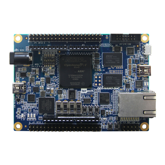
Terasic DE0-NANO-SoC User Manual
Hide thumbs
Also See for DE0-NANO-SoC:
- User manual (80 pages) ,
- Getting started manual (26 pages) ,
- Design manual (100 pages)

Related Manuals for Terasic DE0-NANO-SoC


Summary of Contents for Terasic DE0-NANO-SoC
-
Page 2: Table Of Contents
........37 4.1 Compile Your Design ......................37 4.2 Program the FPGA Device ....................39 4.3 Verify The Hardware ......................45 Appendix Chapter 5 ............48 5.1 Headquarter & Branches ...................... 48 DE0-Nano-SoC www.terasic.com May 18, 2015 My First FPGA... -
Page 3: Chapter 1 Introduction
This tutorial provides comprehensive information that will help you understand how to create a FPGA design and run it on your DE0-Nano-SoC development board. The following sections provide a quick overview of the design flow, explain what you need to get started, and describe what you will learn. -
Page 4: Before You Begin
Quartus II software, you can download it from the Altera web site at www.altera.com/download. ■ You have a DE0-Nano-SoC Development Board on which you will test your project. Using a development board helps you to verify whether your design is really working. - Page 5 Figure 1-3 Driver Software Installation Since the desired driver is not available on the Windows Update Web site, open the Computer Management and select the Device Manager. This leads to the window in Figure 1-4. DE0-Nano-SoC www.terasic.com May 18, 2015 My First FPGA...
- Page 6 Figure 1-4 Device Manager Right click Other devices>Unknown device and select Update Driver Software…This leads to the window in Figure 1-5. Figure 1-5 Update Driver Software DE0-Nano-SoC www.terasic.com May 18, 2015 My First FPGA...
- Page 7 C:\altera\14.1\quartus\drivers\usb-blaster-ii. Click OK and then upon returning to Figure 1-6.click Next. Figure 1-7 Browse to find the location The driver will now be installed as indicated in Figure 1-8 Click close and you can start using the DE0-Nano-SoC board. DE0-Nano-SoC www.terasic.com May 18, 2015 My First FPGA...
-
Page 8: What You Will Learn
— This design is easy to create and gives you visual feedback that the design works. Of course, you can use your DE0-Nano-SoC board to run other designs as well. For the LED design, you will write Verilog HDL code for a simple 32-bit counter, add a phase-locked loop (PLL) megafunction as the clock source, and add a 2-input multiplexer megafunction. -
Page 9: Assign The Device
1. In the Quartus II software, select File > New Project Wizard. The Introduction page opens. See Figure 2-1. Figure 2-1 New Project Wizard introduction DE0-Nano-SoC www.terasic.com May 18, 2015 My First FPGA... - Page 10 What is the name of this project? Type my_first_fpga. e. What is the name of the top-level design entity for this project? Type my_first_fpga. See Figure 2-2. Figure 2-2 Project information f. Click Next. DE0-Nano-SoC www.terasic.com May 18, 2015 My First FPGA...
- Page 11 2-3. Figure 2-3 Specify the Device Example h. Click Finish. When prompted, choose Yes to create the my_first_fpga project directory. You just created your first Quartus II FPGA project. See Figure 2-4. DE0-Nano-SoC www.terasic.com May 18, 2015 My First FPGA...
- Page 12 Figure 2-4 my_first_fpga project DE0-Nano-SoC www.terasic.com May 18, 2015 My First FPGA...
-
Page 13: Chapter 3 Design Entry
Choose File > New > Block Diagram/Schematic File (see Figure 3-1 to create a new file, Block1.bdf, which you will save as the top-level design. Figure 3-1 New BDF Click OK. DE0-Nano-SoC www.terasic.com May 18, 2015 My First FPGA... - Page 14 Click OK to create a new file Verilog1.v, which you will save as simple_counter.v. Select File > Save As and enter the following information (see Figure 3-3). File name: simple_counter.v Save as type: Verilog HDL File (*.v, *.vlg, *.verilog) DE0-Nano-SoC www.terasic.com May 18, 2015 My First FPGA...
- Page 15 //It has a single clock input and a 32-bit output port module simple_counter ( CLOCK_50, counter_out input CLOCK_50 ; output [31:0] counter_out; [31:0] counter_out; always @ (posedge CLOCK_50) // on positive clock edge DE0-Nano-SoC www.terasic.com May 18, 2015 My First FPGA...
- Page 16 Symbol File (.sym).You use this Symbol File to add the HDL code to your BDF schematic. The Quartus II software creates a Symbol File and displays a message (see Figure 3-5). DE0-Nano-SoC www.terasic.com May 18, 2015 My First FPGA...
- Page 17 16. Click OK. Move the cursor to the BDF grid; the symbol image moves with the cursor. Click to place the simple_counter symbol onto the BDF. You can move the block after placing it by simply clicking DE0-Nano-SoC www.terasic.com May 18, 2015...
- Page 18 This tutorial design uses a PLL clock source to drive a simple counter. A PLL uses the on-board oscillator (DE0-Nano-SoC Board is 50 MHz) to create a constant clock frequency as the input to the counter. To create the clock source, you will add a pre-built LPM megafunction named Altera PLL.
- Page 19 Selection Altera PLL in the Library/Clocks/PLL , click "+Add" bar. See Figure 3-9 Under IP variation file type, Choose Verilog HDL. Under IP variation file, Type pll.v at the end of the already create directory name. Click OK. DE0-Nano-SoC www.terasic.com May 18, 2015 My First FPGA...
- Page 20 Figure 3-9 IP Catalog Selections In the Altera PLL windows, make the following selections (see Figure 3-10). The device speed grade choose 6 for DE0-Nano-SoC. Set the frequency of the refclk input 50 MHz. DE0-Nano-SoC www.terasic.com May 18, 2015 My First FPGA...
- Page 21 As you turn it off, pin disappear from the PLL block’s graphical preview. See Figure 3-11 for an example. Figure 3-11 Selections of Altera PLL windows Then, make the following selection (see Figure 3-12). DE0-Nano-SoC www.terasic.com May 18, 2015 My First FPGA...
- Page 22 Figure 3-12 Selections of Altera PLL windows 8. Click Finish It leads to Figure 3-13.Click Exit. Figure 3-13 PLL Generation 9. The Symbol window opens, showing the newly created PLL megafunction. See Figure 3-14. DE0-Nano-SoC www.terasic.com May 18, 2015 My First FPGA...
- Page 23 10. Click OK and place the pll symbol onto the BDF to the left of the simple_counter symbol. You can move the symbols around by holding down the left mouse button, helping you ensure that they line up properly. See Figure 3-15. Figure 3-15 Place the PLL Symbol DE0-Nano-SoC www.terasic.com May 18, 2015 My First FPGA...
- Page 24 Figure 3-17 Click OK If you need more room to place symbols, you can use the vertical and horizontal scroll bars at the edges of the BDF window to view more drawing space. DE0-Nano-SoC www.terasic.com May 18, 2015 My First FPGA...
- Page 25 Using the Orthogonal Bus tool, draw a bus line connected on one side to the simple_counter output port, and leave the other end unconnected at about 4 to 8 grid spaces to the right of the simple_counter. DE0-Nano-SoC www.terasic.com May 18, 2015...
- Page 26 BDF schematics, where X is the most significant bit (MSB) and Y is the least significant bit (LSB). Click OK. Figure 3-21 shows the BDF. DE0-Nano-SoC www.terasic.com May 18, 2015 My First FPGA...
- Page 27 Figure 3-20 Change the output BUS name Figure 3-21 BDF DE0-Nano-SoC www.terasic.com May 18, 2015 My First FPGA...
-
Page 28: Add A Multiplexer
This design uses a multiplexer to route the simple_counter output to the LED pins on the DE0-Nano-SoC development board. You will use the MegaWizard Plug-In Manager to add the multiplexer, lpm_mux. The design multiplexes two variations of the counter bus to four LEDs on the DE0-Nano-SoC development board. - Page 29 Under how wide should the 'data' input and 'result' output be? Select 4 (see Figure 3-23). Figure 3-23 lpm_mux settings Click Next. 10. Click Finish twice. The Symbol window appears (see Figure 3-24 for an example). DE0-Nano-SoC www.terasic.com May 18, 2015 My First FPGA...
- Page 30 13. Add input buses and output pins to the counter_bus_mux symbol as follows: Using the Orthogonal Bus tool, draw bus lines from the data1x[3..0] and data0x[3..0]. Input ports to about 8 to 12 grid spaces to the left of counter_bus_mux. DE0-Nano-SoC www.terasic.com May 18, 2015...
- Page 31 If you have not done so yet, have your project file before continuing. 14. Choose Edit > Insert Symbol. 15. Under Libraries, double-click quartus/libraries/ > primitives > pin > output (see Figure 3-27). DE0-Nano-SoC www.terasic.com May 18, 2015 My First FPGA...
- Page 32 19. Attach an input pin to the multiplexer select line using an input pin: Choose Edit > Insert Symbol. Under Libraries, double-click quartus/libraries/ > primitives > pin > input. Click OK. 20. Place this input pin below counter_bus_mux. DE0-Nano-SoC www.terasic.com May 18, 2015 My First FPGA...
- Page 33 25. Under Libraries, double-click quartus/libraries/ > primitives >logic > not (see Figure 3-30). 26. Click OK. 27. Place this not pin so that it connects to KEY[1] and the pll rst (see Figure 3-31). Figure 3-29 Adding the KEY [1:0] Input Pin DE0-Nano-SoC www.terasic.com May 18, 2015 My First FPGA...
- Page 34 Text tool on the toolbar (indicated with the A symbol). For example, you can add the label “OFF = SLOW, ON = FAST” to the KEY [0] input pin and add a project description, such as “My First FPGA Project.” DE0-Nano-SoC www.terasic.com May 18, 2015...
-
Page 35: Assign The Pins
Figure 3-32 Pin Planner Example In the Location column next to each of the seven node names, add the coordinates (pin numbers) as shown in Table 3-1 for the actual values to use with your DE0-Nano-SoC board. DE0-Nano-SoC www.terasic.com May 18, 2015... - Page 36 Group. Each bank has a distinct color, which corresponds to the top-view wire bond drawing in the upper right window. See Figure 3-33. Figure 3-33 Completed Pin Planning Example Now, you are finished creating your Quartus II design! DE0-Nano-SoC www.terasic.com May 18, 2015 My First FPGA...
-
Page 37: Create A Default Timequest Sdc File
Choose File > New SDC file. The SDC editor opens. Type the following code into the editor: create_clock -name "CLOCK_50" -period 20.000ns [get_ports {CLOCK_50}] derive_pll_clocks derive_clock_uncertainty Save this file as my_first_fpga.sdc (see Figure 3-34). Figure 3-34 Default SDC DE0-Nano-SoC www.terasic.com May 18, 2015 My First FPGA... - Page 38 Naming the SDC with the same name as the top-level file except for the .sdc extension causes the Quartus II software to using this timing analysis file automatically by default. If you used another name, you would need to add the SDC to the assignments file list. DE0-Nano-SoC www.terasic.com May 18, 2015...
-
Page 39: Compile And Verify Your Design
In the Processing menu, choose Start Compilation or click the Play button on the toolbar. If you are asked to save changes to your BDF, click Yes. While compiling your design, the Quartus II software provides useful information about the compilation (see Figure 4-1). DE0-Nano-SoC www.terasic.com May 18, 2015 My First FPGA... - Page 40 I/O pins used for the LEDs were not set. The software provides the compilation results in the Compilation Report tab as shown in Figure 4-2. DE0-Nano-SoC www.terasic.com May 18, 2015 My First FPGA...
-
Page 41: Program The Fpga Device
Connect the power supply cable to your board and to a power outlet. For the DE0-Nano-SoC board, connect the USB-BlasterII (included in your development kit) to J13 and the USB cable to the USB-BlasterII. Connect the other end of the USB cable to the host computer. - Page 42 Figure 4-3 Programmer Window Click Hardware Setup. If it is not already turned on, turn on the DE0-Nano-SoC [USB-1] option under currently selected hardware. See Figure 4-4. DE0-Nano-SoC www.terasic.com May 18, 2015 My First FPGA...
- Page 43 Figure 4-4 Hardware Setting Click Close. Click Auto Detect to detect all the devices on the JTAG chain. Select 5CSEMA4 and click OK. DE0-Nano-SoC www.terasic.com May 18, 2015 My First FPGA...
- Page 44 Click Yes to match device list. Figure 4-6 Warning for device list not match Both HPS and FPGA will be list on the programmer. Select FPGA device and click Change File a .sof file. DE0-Nano-SoC www.terasic.com May 18, 2015 My First FPGA...
- Page 45 Figure 4-7 Programmer window Selecting the my_first_fpga.sof file from the project directory (see Figure select to Program/Configure and click Start to program .sof file into FPGA. DE0-Nano-SoC www.terasic.com May 18, 2015 My First FPGA...
- Page 46 Congratulations, you have created, compiled, and programmed your first FPGA design! The compiled SRAM Object File (.sof) is loaded onto the FPGA on the development board and the design should be running. DE0-Nano-SoC www.terasic.com May 18, 2015 My First FPGA...
-
Page 47: Verify The Hardware
Pressing this KEY causes the design to multiplex using the faster advancing part of the counter (bits [24..21]). If other LEDs emit faintness light, Choose Assignments > Device. Click Device and Pin Options. See Figure 4-8. DE0-Nano-SoC www.terasic.com May 18, 2015 My First FPGA... - Page 48 Figure 4-8 Device and Options Choose Unused Pins. Reserve all unused pins: Choose the As input tri-stated option. See Figure 4-9. DE0-Nano-SoC www.terasic.com May 18, 2015 My First FPGA...
- Page 49 In the Processing menu, choose Start Compilation. After the compile, Choose Tools > Programmer. Select the my_first_fpga.sof file from the project directory. Click Start. At this time you could find the other LEDs are unlighted. DE0-Nano-SoC www.terasic.com May 18, 2015...
-
Page 50: Chapter 5 Appendix
Chapter 5 Appendix & & Tel :+886-3-575-0880 Fax :+886-3-572-6690 Add:9F, No.176, Sec.2, Gongdao 5th Rd, East Dist, Hsinchu City, Taiwan 300-70 Email:sales@terasic.com / support@terasic.com DE0-Nano-SoC www.terasic.com May 18, 2015 My First FPGA...
Need help?
Do you have a question about the DE0-NANO-SoC and is the answer not in the manual?
Questions and answers