Table of Contents
Advertisement
Quick Links
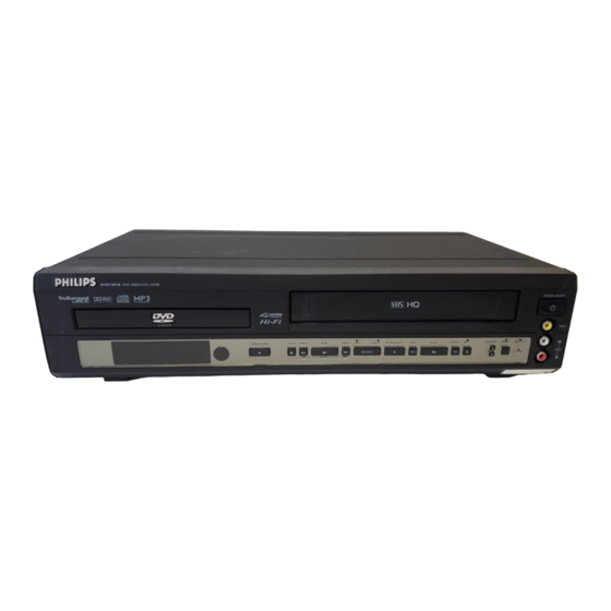
DVD-Video Player
©
Copyright 2002 Philips Consumer Electronics B.V. Eindhoven, The Netherlands.
All rights reserved. No part of this publication may be reproduced, stored in a
retrieval system or transmitted, in any form or by any means, electronic,
mechanical, photocopying, or otherwise without the prior permission of Philips.
Published by MW 0269 Service PaCE
Contents
Laser Beam Safety Precautions
Important Safety Precautions
Preparation for Servicing
Standart Notes for Servicing
Operating Controls and Functions
Signal Name Abbreviations
Cabinet Disassembly Instructions
Electrical Adjustment Instructions
Firmware Renewal Mode
Block Diagrams
Schematic Diagrams/CBA's and Test Points
Waveforms
Wiring Diagram
System Control Timing Charts
IC Pin Function Descriptions
Lead Identifications
Exploded Views
Spare Parts List
Printed in the Netherlands
DVD740VR /001 /051
Page
1-1-1
1-2-1
1-3-1
1-4-1
1-5-1
1-6-1
1-7-1
1-8-1
1-9-1
1-10-1
1-11-1
1-12-1
1-13-1
1-14-1
1-15-1
1-16-1
1-18-1
Subject to modification
DVD740VR
EN 3122 785 12940
Advertisement
Table of Contents

Related Manuals for Philips DVD740VR/051


Summary of Contents for Philips DVD740VR/051
- Page 1 All rights reserved. No part of this publication may be reproduced, stored in a retrieval system or transmitted, in any form or by any means, electronic, mechanical, photocopying, or otherwise without the prior permission of Philips. Published by MW 0269 Service PaCE...
-
Page 2: Main Section
MAIN SECTION DIGITAL VIDEO DISC PLAYER & VIDEO CASSETTE RECORDER Sec. 1: Main Section I Adjustment Procedures I Schematic Diagrams and CBA’s I Exploded Views I Mechanical and Electrical Parts List... -
Page 3: Laser Beam Safety Precautions
LASER BEAM SAFETY PRECAUTIONS This DVD player uses a pickup that emits a laser beam. Do not look directly at the laser beam coming from the pickup or allow it to strike against your skin. The laser beam is emitted from the location shown in the figure. When checking the laser diode, be sure to keep your eyes at least 30cm away from the pickup lens when the diode is turned on. -
Page 4: Important Safety Precautions
IMPORTANT SAFETY PRECAUTIONS Product Safety Notice I. Also check areas surrounding repaired locations. J. Use care that foreign objects (screws, solder drop- Some electrical and mechanical parts have special lets, etc.) do not remain inside the set. safety-related characteristics which are often not evi- K. -
Page 5: Safety Check After Servicing
Safety Check after Servicing Chassis or Secondary Conductor Examine the area surrounding the repaired location for damage or deterioration. Observe that screws, parts, and wires have been returned to their original posi- Primary Circuit Terminals tions. Afterwards, do the following tests and confirm the specified values to verify compliance with safety standards. -
Page 6: Standard Notes For Servicing
STANDARD NOTES FOR SERVICING Circuit Board Indications How to Remove / Install Flat Pack-IC a. The output pin of the 3 pin Regulator ICs is indi- 1. Removal cated as shown. With Hot-Air Flat Pack-IC Desoldering Machine:. (1) Prepare the hot-air flat pack-IC desoldering Top View Bottom View machine, then apply hot air to the Flat Pack-IC... - Page 7 With Soldering Iron: (4) Bottom of the flat pack-IC is fixed with glue to the CBA; when removing entire flat pack-IC, first apply (1) Using desoldering braid, remove the solder from all soldering iron to center of the flat pack-IC and heat pins of the flat pack-IC.
- Page 8 Instructions for Handling 2. Installation Semi-conductors (1) Using desoldering braid, remove the solder from the foil of each pin of the flat pack-IC on the CBA so Electrostatic breakdown of the semi-conductors may you can install a replacement flat pack-IC more occur due to a potential difference caused by electro- easily.
-
Page 9: Preparation For Servicing
PREPARATION FOR SERVICING How to Enter the Service Mode About REC-Safety Switch Caution: The REC-Safety Switch is directly mounted on the About Optical Sensors Main CBA. When the Deck Mechanism Assembly is Caution: removed from the Main CBA for servicing, this switch does not work automatically. - Page 10 OPERATING CONTROLS AND FUNCTIONS [ DVD740VR/001 ] 1-5-1 H9330IB...
- Page 11 1-5-2 H9330IB...
- Page 12 1-5-3 H9330IB...
- Page 13 1-5-4 H9330IB...
- Page 14 1-5-5 H9330IB...
- Page 15 [ DVD740VR/051 ] 1-5-6 H9330IB...
- Page 16 1-5-7 H9330IB...
- Page 17 1-5-8 H9330IB...
- Page 18 1-5-9 H9330IB...
- Page 19 1-5-10 H9330IB...
- Page 20 SIGNAL NAME ABBREVIATIONS Signal Name Function Signal Name Function Color Phase Rotary Changeover C-ROTA SIgnal SCART 1 8Pin Output Control 8POUT-1 Signal C-SYNC Composite Synchronized Pulse SCART 2 8Pin Output Control CAS LED “CASSETTE” LED Signal Output 8POUT-2 Signal CLKSEL Clock Select (GND) A-COM Audio Head Common...
- Page 21 Signal Name Function Signal Name Function REC LED “REC” LED Signal Output Comparator Input of Video Signal FTV-IN for Follow TV Recording Safety SW Detect (With REC-SAF-SW Record tab=”L”/ With out Record H-A-COMP Head Amp Comparator Signal tab=”H”) H-A-SW Video Head Amp Switching Pulse REMOTE Remote Control Sensor Hi-Fi-A (L)
-
Page 22: Cabinet Disassembly Instructions
CABINET DISASSEMBLY INSTRUCTIONS 1. Disassembly Flowchart REMOVAL REMOVE/*UNHOOK/ This flowchart indicates the disassembly steps to gain LOC. PART Fig. UNLOCK/RELEASE/ Note access to item(s) to be serviced. When reassembling, UNPLUG/DESOLDER follow the steps in reverse order. Bend, route, and dress the cables as they were originally. DVD Main 3(S-5), *CN101, [1] Top Cover... - Page 23 Reference Notes CAUTION 1: Locking Tabs (L-1) and (L-2) are fragile. [1] Top Cover Be careful not to break them. (S-1) (S-1) 1-1. Connect the wall plug to an AC outlet and press the OPEN/CLOSE button to open the Tray. 1-2.
- Page 24 (S-4) CN701 (S-7) CN501 [7] Rear Panel (S-4) (S-6) (S-7) [5] DVD Mecha Assembly Fig. D6 Fig. D4 (S-8) (S-5) (S-9) (S-5) CN101 [6] DVD Main (S-5) (S-8) CBA Unit (S-8) (S-9) CN401 [8] VCR Chassis DVD Mecha Unit Assembly CN002 Short the three short lands by soldering CN001...
- Page 25 FE Head Cylinder Assembly AC Head Assembly SW507 LD-SW [9] Deck Assembly [10] Main CBA [12] AFV CBA CN2002 [9] Deck Assembly Cam Gear Hole Shaft Desolder Hole Desolder [11] Function CBA LD-SW from bottom [10] Main CBA (S-10) [10] Main CBA From Cylinder From...
- Page 26 Bracket (S-11) (S-12) (S-11) [13] Power Supply CBA (W-1) (S-13) [15] Deck Pedestal-2 (L-3) (W-1) [17] Insulator (W-1) [16] Side Bracket [14] Deck Pedestal-1 (S-14) Fig. D9 HOW TO MANUAL EJECT 1. Remove the Top Case. 2. Make a tool from a paper clip, etc., (length = approxi- mately 50 mm, maximum diameter = approximately 3 mm) as shown below.
-
Page 27: Electrical Adjustment Instructions
ELECTRICAL ADJUSTMENT INSTRUCTIONS General Note: "CBA" is an abbreviation for "Circuit Board Assembly." NOTE: Figure 1 1.Electrical adjustments are required after replacing circuit components and certain mechanical parts. It is important to do these adjustments only after EXT. Syncronize Trigger Point all repairs and replacements have been com- V-Sync pleted. -
Page 28: Firmware Renewal Mode
FIRMWARE RENEWAL MODE 1. Turn the power on and remove the disc on the tray. 2. To put the DVD player into version up mode, press [9], [8], [7], [6], and [SEARCH MODE] buttons on the remote control unit in that order. The tray will open automatically. - Page 29 BLOCK DIAGRAMS <VCR Section> Servo/System Control Block Diagram TEST POINT INFORMATION :INDICATES A TEST POINT WITH A JUMPER WIRE ACROSS A HOLE IN THE PCB. IC501 FRONT JACK CBA :USED TO INDICATE A TEST POINT WITH A COMPONENT LEAD ON FOIL SIDE. (SERVO/SYSTEM CONTROL) :USED TO INDICATE A TEST POINT WITH NO TEST PIN.
-
Page 30: Video Block Diagram
Video Block Diagram NOTE FOR WIRE CONNECTORS: " " = SMD TEST POINT INFORMATION 1. PREFIX SYMBOL "CN" MEANS CONNECTOR. :INDICATES A TEST POINT WITH A JUMPER WIRE ACROSS A HOLE IN THE PCB. (CAN DISCONNECT AND RECONNECT.) :USED TO INDICATE A TEST POINT WITH A COMPONENT LEAD ON FOIL SIDE. 2. -
Page 31: Audio Block Diagram
Audio Block Diagram NOTE FOR WIRE CONNECTORS: " " = SMD 1. PREFIX SYMBOL "CN" MEANS CONNECTOR. (CAN DISCONNECT AND RECONNECT.) 2. PREFIX SYMBOL "CL" MEANS WIRE-SOLDER HOLES OF THE PCB. (WIRE IS SOLDERED DIRECTLY.) PB-AUDIO SIGNAL REC-AUDIO SIGNAL Mode : SP/REC MAIN CBA N-A-PB TO Hi-Fi... - Page 32 Hi-Fi Audio Block Diagram NOTE FOR WIRE CONNECTORS: 1. PREFIX SYMBOL "CN" MEANS CONNECTOR. " " = SMD (CAN DISCONNECT AND RECONNECT.) 2. PREFIX SYMBOL "CL" MEANS WIRE-SOLDER HOLES OF THE PCB. DVD AUDIO SIGNAL PB-AUDIO SIGNAL REC-AUDIO SIGNAL Mode : SP/REC (WIRE IS SOLDERED DIRECTLY.) IC751 (SW) JK101...
-
Page 33: Power Supply Block Diagram
Power Supply Block Diagram NOTE : CAUTION CAUTION ! FOR CONTINUED PROTECTION AGAINST FIRE HAZARD, Fixed voltage (or Auto voltage selectable ) power supply circuit is used in this unit. The voltage for parts in hot circuit is measured using If Main Fuse (F001) is blown, check to see that all components in the power supply hot GND as a common terminal. - Page 34 BLOCK DIAGRAMS < DVD Section > DVD System Control Block Diagram NOTE FOR WIRE CONNECTORS: 1. PREFIX SYMBOL "CN" MEANS CONNECTOR. (CAN DISCONNECT AND RECONNECT.) " " = SMD 2. PREFIX SYMBOL "CL" MEANS WIRE-SOLDER HOLES OF THE PCB. (WIRE IS SOLDERED DIRECTLY.) IC601 (DVD HOST PROCESSOR) IC2001...
- Page 35 RF Signal Process/Servo Block Diagram NOTE FOR WIRE CONNECTORS: 1. PREFIX SYMBOL "CN" MEANS CONNECTOR. " " = SMD (CAN DISCONNECT AND RECONNECT.) 2. PREFIX SYMBOL "CL" MEANS WIRE-SOLDER HOLES OF THE PCB. (WIRE IS SOLDERED DIRECTLY.) DATA(VIDEO/AUDIO) SIGNAL FOCUS SERVO SIGNAL TRACKING SERVO SIGNAL SLIDE SERVO SIGNAL DISK SERVO SIGNAL...
- Page 36 DVD Signal Process Block Diagram NOTE FOR WIRE CONNECTORS: " " = SMD 1. PREFIX SYMBOL "CN" MEANS CONNECTOR. (CAN DISCONNECT AND RECONNECT.) 2. PREFIX SYMBOL "CL" MEANS WIRE-SOLDER HOLES OF THE PCB. (WIRE IS SOLDERED DIRECTLY.) DATA(VIDEO/AUDIO) SIGNAL DVD MAIN CBA UNIT IC201 (DVD SIGNAL PROCESS) PARA0 PARA1...
- Page 37 DVD Video Block Diagram NOTE FOR WIRE CONNECTORS: " " = SMD 1. PREFIX SYMBOL "CN" MEANS CONNECTOR. (CAN DISCONNECT AND RECONNECT.) 2. PREFIX SYMBOL "CL" MEANS WIRE-SOLDER DATA(VIDEO) SIGNAL DATA(AUDIO) SIGNAL VIDEO SIGNAL DATA(VIDEO/AUDIO) SIGNAL HOLES OF THE PCB. (WIRE IS SOLDERED DIRECTLY.) IC601 (DVD HOST PROCESSOR) CACHE...
- Page 38 DVD Audio Block Diagram NOTE FOR WIRE CONNECTORS: 1. PREFIX SYMBOL "CN" MEANS CONNECTOR. " " = SMD (CAN DISCONNECT AND RECONNECT.) 2. PREFIX SYMBOL "CL" MEANS WIRE-SOLDER HOLES OF THE PCB. (WIRE IS SOLDERED DIRECTLY.) DATA(AUDIO) SIGNAL AUDIO SIGNAL IC1204 FIBER OPTIC TRANS MODULE...
- Page 39 SCHEMATIC DIAGRAMS / CBA'S AND TEST POINTS Main 1/8 Schematic Diagram Parts Location Guide Standard Notes Notes: Ref No. Position Ref No. Position Ref No. Position WARNING 1. Do not use the part number shown on these draw- CAPACITORS COILS RESISTORS ings for ordering.
- Page 40 0.00 ~ 0.51V OUTPUT TIMER IS NOT CONSISTENT HERE. BOTH PLAY & REC MODES. DVD740VR/001 0.51 ~ 0.92V STOP/EJECT POWER DVD740VR/051 0.92 ~ 1.27V CH UP 1.27 ~ 1.61V PLAY CH DOWN 1.61 ~ 1.98V ----------------------------- 1.98 ~ 2.39V REC/OTR ----------------------------- 2.39 ~ 2.90V...
- Page 41 Models and Marks (2.5) THE SAME VOLTAGE FOR INDICATES THAT THE VOLTAGE MODEL MARK BOTH PLAY & REC MODES. IS NOT CONSISTENT HERE. DVD740VR/001 DVD740VR/051 MAIN 2/8 Schematic Diagram Parts Location Guide Ref No. Position CAPACITORS C701 C703 C706 C708...
- Page 42 Main 3/8 Schematic Diagram < VCR Section > MODE: SP/REC “ “ = SMD PLAY MODE REC MODE (2.5) THE SAME VOLTAGE FOR INDICATES THAT THE VOLTAGE BOTH PLAY & REC MODES. IS NOT CONSISTENT HERE. MAIN 3/8 Schematic Diagram Parts Location Guide Ref No.
- Page 43 Main 4/8 Schematic Diagram < VCR Section > “ “ = SMD MODE: SP/REC PLAY MODE REC MODE (2.5) THE SAME VOLTAGE FOR INDICATES THAT THE VOLTAGE BOTH PLAY & REC MODES. IS NOT CONSISTENT HERE. 1-11-12 1-11-13 1-11-14 H9330SCM4...
- Page 44 Main 5/8 Schematic Diagram Parts Location Guide Main 4/8 Schematic Diagram Parts Location Guide MAIN 4/8 Schematic Diagram Parts Location Guide MAIN 5/8 Schematic Diagram Parts Location Guide Ref No. Position Ref No. Position Ref No. Position Ref No. Position CAPACITORS TRANSISTORS CAPACITORS...
- Page 45 Main 5/8 Schematic Diagram < VCR Section > MODE: SP/REC PLAY MODE REC MODE (2.5) INDICATES THAT THE VOLTAGE THE SAME VOLTAGE FOR IS NOT CONSISTENT HERE. BOTH PLAY & REC MODES. “ “ = SMD H9330SCM5 1-11-17 1-11-18...
- Page 46 Main 6/8 Schematic Diagram < VCR Section > MAIN 6/8 Schematic Diagram Parts Location Guide Ref No. Position Ref No. Position CAPACITORS TRANSISTORS MODE: SP/REC “ “ = SMD PLAY MODE C1201 BB-1 Q1501 EE-3 REC MODE (2.5) C1202 BB-1 Q1502 EE-3 INDICATES THAT THE VOLTAGE...
- Page 47 Main 7/8 Schematic Diagram < VCR Section > “ “ = SMD MODE: SP/REC PLAY MODE REC MODE (2.5) INDICATES THAT THE VOLTAGE THE SAME VOLTAGE FOR IS NOT CONSISTENT HERE. BOTH PLAY & REC MODES. MAIN 7/8 Schematic Diagram Parts Location Guide Ref No.
- Page 48 Main 8/8 Schematic Diagram < VCR Section > MODE: SP/REC PLAY MODE “ “ = SMD REC MODE (2.5) THE SAME VOLTAGE FOR INDICATES THAT THE VOLTAGE IS NOT CONSISTENT HERE. BOTH PLAY & REC MODES. MAIN 8/8 Schematic Diagram Parts Location Guide Ref No.
- Page 49 AC plug to the AC power supply. BOTH PLAY & REC MODES. IS NOT CONSISTENT HERE. CAUTION DVD740VR/051 Otherwise it may cause some components in the power supply circuit to fail. “ “ = SMD FOR CONTINUED PROTECTION AGAINST FIRE HAZARD, REPLACE ONLY WITH THE SAME TYPE FUSE.
- Page 50 Function Schematic Diagram < VCR Section > FL2001 MATRIX CHART MODE: SP/REC PLAY MODE “ “ = SMD REC MODE (2.5) STANDBY INDICATES THAT THE VOLTAGE THE SAME VOLTAGE FOR REPEAT IS NOT CONSISTENT HERE. BOTH PLAY & REC MODES. STANDBY TITLE CHP.
- Page 51 Front Jack Schematic Diagram < VCR Section > MODE: SP/REC PLAY MODE REC MODE Note: (2.5) When it is necessary to replace one or more of the following Diodes, INDICATES THAT THE VOLTAGE THE SAME VOLTAGE FOR all four should be replaced: D652, D653, D654, D655. IS NOT CONSISTENT HERE.
- Page 52 AFV Schematic Diagram < VCR Section > MODE: SP/REC PLAY MODE “ “ = SMD REC MODE (2.5) INDICATES THAT THE VOLTAGE THE SAME VOLTAGE FOR IS NOT CONSISTENT HERE. BOTH PLAY & REC MODES. AFV Schematic Diagram Parts Location Guide Ref No.
- Page 53 Main CBA Parts Location Guide Ref No. Position Ref No. Position Ref No. Position Ref No. Position Ref No. Position Ref No. Position Ref No. Position Ref No. Position Ref No. Position Ref No. Position Ref No. Position CAPACITORS CAPACITORS CAPACITORS CAPACITORS DIODES...
- Page 54 Main CBA Top View Sensor CBA Top View ( End Sensor ) BHB300F01011-A TP751 V-OUT BHB300F01011-B TP301 C-PB Sensor CBA Top View ( Start Sensor ) BHB300F01011-A BHB300F01011-B TP502 END-S VR501 SW-P TP503 TP504 RF-SW TP501 S-INH 1-11-35 1-11-36 1-11-37 BH9311F01012-A...
- Page 55 Main CBA Bottom View POWER SUPPLY CBA Parts Location Guide Ref No. Position Ref No. Position CAPACITORS DIODES C013 D1041 C018 D1042 C019 D1043 C1001 C1002 IC1001 C1003 IC1002 C1004 IC1041 C1005 COILS C1006 J922 C1007 L008 C1008 L1001 C1009 L1002 C1012 L1003...
- Page 56 Power Supply CBA Top View Power Supply CBA Bottom View CAUTION ! BECAUSE A HOT CHASSIS GROUND IS PRESENT IN THE POWER NOTE : CAUTION Fixed voltage ( or Auto voltage selectable ) power supply circuit is used in this unit. SUPPLY CIRCUIT , AN ISOLATION TRANSFORMER MUST BE USED.
- Page 57 Function CBA Top View FUNCTION CBA Parts Location Guide Ref No. Position CAPACITORS C2001 C2002 C2004 C2010 C2012 C2055 CONNECTORS CL2004 CN2001 DIODES D2001 D2003 D2004 D2005 IC2001 COILS L2001 L2003 L2004 Function CBA Bottom View TRANSISTOR Q2022 RESISTORS R1041 R2001 R2002 R2003...
- Page 58 Front Jack CBA Top View Front Jack CBA Bottom View FRONT JACK CBA Parts Location Guide Ref No. Position CAPACITORS C651 C652 CONNECTOR CN651 DIODES D651 D652 D653 RESISTORS R651 R652 R653 R654 R655 R656 SWITCHES SW651 SW652 SW653 SW654 MISCELLANEOUS JK651 JK652...
- Page 59 AFV CBA Top View AFV CBA Bottom View Junction-A CBA Top View Junction-A CBA Bottom View BH9311F01012-E Junction-B CBA Top View Junction-B CBA Bottom View BHC400F01091 AFV CBA Parts Location Guide Ref No. Position Ref No. Position Ref No. Position CAPACITORS CAPACITORS COILS...
- Page 60 DVD Main 1/4 Schematic Diagram < DVD Section > “ “ = SMD MODE: SP/REC PLAY MODE REC MODE (2.5) THE SAME VOLTAGE FOR INDICATES THAT THE VOLTAGE BOTH PLAY & REC MODES. IS NOT CONSISTENT HERE. 1-11-49 1-11-50 1-11-51 H9330SCD1...
- Page 61 DVD Main 2/4 Schematic Diagram < DVD Section > MODE: SP/REC “ “ = SMD PLAY MODE REC MODE (2.5) THE SAME VOLTAGE FOR INDICATES THAT THE VOLTAGE BOTH PLAY & REC MODES. IS NOT CONSISTENT HERE. H9330SCD2 1-11-52 1-11-53 1-11-54...
- Page 62 DVD Main 3/4 Schematic Diagram < DVD Section > MODE: SP/REC “ “ = SMD PLAY MODE REC MODE (2.5) THE SAME VOLTAGE FOR INDICATES THAT THE VOLTAGE BOTH PLAY & REC MODES. IS NOT CONSISTENT HERE. 1-11-55 1-11-56 1-11-57 H9330SCD3...
- Page 63 DVD Main 4/4 Schematic Diagram < DVD Section > MODE: SP/REC “ “ = SMD PLAY MODE REC MODE (2.5) INDICATES THAT THE VOLTAGE THE SAME VOLTAGE FOR IS NOT CONSISTENT HERE. BOTH PLAY & REC MODES. 1-11-58 1-11-60 1-11-59 H9330SCD4...
- Page 64 WAVEFORMS WAVEFORMS NOTE: Input CD: 1kHz PLAY (WF4~WF6) DVD: POWER ON (STOP) MODE (WF1~WF3) (TP751 of Main CBA) Pin 5 of CN1601 Pin 13 of CN1601 V-OUT E-E 10usec 50mV x 10 VIDEO-Y 0.2V 20usec AUDIO-L 0.5msec (TP751 of Main CBA) UPPER (TP302 of Main CBA) LOWER...
- Page 65 WIRING DIAGRAM < VCR SECTION > NOTE FOR WIRE CONNECTORS: 1. PREFIX SYMBOL "CN" MEANS CONNECTOR. REAR (CAN DISCONNECT AND RECONNECT.) S-VIDEO DIGITAL AUDIO AUDIO 2. PREFIX SYMBOL "CL" MEANS WIRE-SOLDER HOLES OF THE PCB. AUDIO OUT OUT (R) OUT (L) ANT-IN ANT-OUT (WIRE IS SOLDERED DIRECTLY.)
- Page 66 WIRING DIAGRAM< DVD SECTION> DVD MECHA LOADING RELAY CBA MOTOR CN501 P-ON+1.8V 1 P-ON+1.8V 2 EV+2.5V 3 TRAY-OUT CN3001 CN401 EV+2.5V 4 1 LM(+) P-ON+5V 2 LM(-) P-ON+5V 6 SPINDLE SW CBA TRAY-IN 3 TRAY-IN MOTOR GND 7 4 TRAY-OUT GND 8 5 GND GND 9...
-
Page 67: System Control Timing Charts
SYSTEM CONTROL TIMING CHARTS Mode SW : LD-SW LD-SW Position detection A/D Input voltage Limit Symbol (Calculated voltage) 3.76V~4.50V (4.12V) 4.51V~5.00V (5.00V) 0.00V~0.25V (0.00V) 1.06V~1.50V (1.21V) 0.66V~1.05V (0.91V) 1.99V~2.60V (2.17V) 1.51V~1.98V (1.80V) 3.20V~3.75V (3.40V) 0.26V~0.65V (0.44V) 4.51V~5.00V (5.00V) 2.61V~3.19V (2.97V) Note : Note: RS: Loading FWD (LM-FWD “H”, LM-REV “L”) - Page 68 18 RF-SW The first rise of RF-SW after a rise in F-AD signal F-AD (Internal Signal) "H" "H" "Z" 5 C-DRIVE "L" "L" Stop detection (T2) Acceleration Detection (T1) Slow Tracking Value PB CTL Reversal Limit Value 78 C-F/R 16 H-A-SW 15 ROTA STILL FRAME ADVANCE...
- Page 69 18 RF-SW The first rise of RF-SW after a rise in F-AD signal F-AD (Internal Signal) "H" "H" "Z" 5 C-DRIVE "L" "L" Stop detection (T2) Acceleration Detection (T1) Slow Tracking Value PB CTL Reversal Limit Value 78 C-F/R 16 H-A-SW 15 ROTA STILL FRAME ADVANCE...
- Page 70 EJECT ST-S,/ END-S "OFF" CASS.LOAD LD-FWD 0.2S LD-REV 0.7S LD-FWD 0.2S LD-REV 0.2S LD-FWD 0.5S LD-REV STOP(A) PLAY LD-FWD PLAY LD-FWD LD-REV 0.2S LD-FWD PLAY PLAY PAUSE (SLOW) LD-FWD STILL(SLOW) PLAY LD-REV 0.2S LD-FWD PLAY STOP /EJECT LD-REV STOP(A) Fig. 3 1-14-4 H9330TI...
- Page 71 STOP(A) STOP LD-REV 0.2S LD-FWD STOP /EJECT LD-REV 2.0S LD-FWD 0.5S LD-REV STOP(A) LD-REV 0.2S LD-FWD STOP /EJECT LD-REV 2.0S LD-FWD 0.5S LD-REV STOP(A) LD-FWD PAUSE LD-FWD 2.5S Short REV LD-REV 0.2S LD-FWD REC PAUSE REC or PAUSE STOP /EJECT LD-FWD 1.5S LD-REV...
-
Page 72: Ic Pin Function Descriptions
IC PIN FUNCTION DESCRIPTIONS [ VCR Section ] Signal Active Function Name Level IC501( SERVO / SYSTEM CONTROL IC ) POWER “POWER” LED 23 OUT Signal Output “H” ≥ 4.5V, “L” ≤ 1.0V “CASSETTE” LED 24 OUT CAS LED Signal Active Signal Output Function... - Page 73 Signal Active Signal Active Function Function Name Level Name Level H/L/ 52 OUT OSD-V- OSD Video Signal 81 OUT LM-FWD/ Loading Motor Output Control Signal Hi-z DVD Power Control DVD- OSDVcc OSDVcc 82 OUT POWER Signal LPF Connected 83 OUT A-MUTE- Audio Mute Control Terminal (Slicer) Signal (Mute = “H”)
- Page 74 IC2001 [ PT6315-S(TP) ] Signal In/Out Name Function Name Clock Input Serial Interface Strobe Key Data 1 Input Key Data 2 Input Power Supply a / KEY-1 Segment Output / Key Souce-1 b / KEY-2 Segment Output / Key Souce-2 Segment Output d / KEY-4 Segment Output/ Key Souce-4...
-
Page 75: Lead Identifications
LEAD IDENTIFICATIONS FS2KM-18A 2SC1815-BL(TPE2) NJM4558D BN1F4M-T KIA78R33PI 2SC1815-Y(TPE2) KIA4558P BA1F4M-T PQ3RD13(1A) 2SC1815-GR(TPE2) KTA1266(GR) 2SC2120-Y(TPE2) KTC3199(Y,GR,BL) KTC3203(Y) 2SC2785(J,H,F,K) KTC3205 (Y) KRC103M 2SA966(Y) KRA103M 2SC2001(K,L) BN1L3Z(P) 2SA1020(Y) KRA110M 2SB892(S) KTA1273(Y) 2SC3266-Y(TPE2) KTA1281(Y) 2SA1015-GR(TPE2) KRA104M BN1L4M-T KRC110M-AT E C B E C B G D S BA1L3Z-T QSZAD0RMB132... -
Page 76: Exploded Views
AC1001 Sensor CBA 2L051 Sensor CBA 2B40 AC1001 2L036 2L022 2L022 2L035 2B39 2B39 2L031 2L022 2B16 [ DVD740VR/051 ] 2L051 2L022 2L062 2L022 2L031 2B39 2L032 2L031 2L052 2L052 2L037 2B13 2B20 Jack CBA JW002 1-18-1... - Page 77 Packing Some Ref. Numbers are not in sequence. [ A ] [ B ] X20A X20B X20C X20D X20E X20J X20F X20G X20H X20I Comparison Chart of Models and Marks Model Mark DVD740VR/001 DVD740VR/051 [ B ] Unit 1-18-3 H9330PEX...
-
Page 78: Table Of Contents
DECK MECHANISM SECTION DIGITAL VIDEO DISC PLAYER & VIDEO CASSETTE RECORDER Sec. 2: Deck Mechanism Section I Standard Maintenance I Mechanism Alignment Procedures I Disassembly / Assembly of Mechanism I Deck Exploded Views I Deck Parts List TABLE OF CONTENTS STANDARD MAINTENANCE . -
Page 79: Standard Maintenance
STANDARD MAINTENANCE Service Schedule of Components H: Hours : Check I: Change Deck Periodic Service Schedule Ref.No. Part Name 1,000 H 2,000 H 3,000 H 4,000 H Cylinder Assembly Loading Motor Assembly Pulley Assembly Tension Lever Sub Assembly AC Head Assembly B573,B574 Reel S, Reel T Capstan Motor... - Page 80 Cleaning Cleaning of Audio Control Head Clean the head with a cotton swab. Cleaning of Video Head Procedure Clean the head with a head cleaning stick or chamois 1.Remove the top cabinet. cloth. 2.Dip the cotton swab in 90% isopropyl alcohol and Procedure clean the audio control head.
-
Page 81: Service Fixture And Tools
SERVICE FIXTURE AND TOOLS J-1-1, J-1-2 Ref. No. Name Part No. Adjustment J-1-1 Alignment Tape FL6A Electrical Adjustments J-1-2 Alignment Tape FL6N8 Azimuth and X Value Adjustment of Audio Control (2 Head model) Head / Adjustment of Envelope Waveform FL6NS8 (4 Head model) Guide Roller Adj.Screwdriver Available... -
Page 82: Mechanical Alignment Procedures
MECHANICAL ALIGNMENT PROCEDURES Explanation of alignment for the tape to correctly run B. Method to place the Cassette Holder in the tape- starts on the next page. Refer to the information below loaded position without a cassette tape on this page if a tape gets stuck, for example, in the 1. -
Page 83: Tape Interchangeability Alignment
1.Tape Interchangeability Alignment Note: To do these alignment procedures, make sure that the Tracking Control Circuit is set to the center position every time a tape is loaded or unloaded. (Refer to page 2-3-4, procedure 1-C, step 2.) Equipment required: Dual Trace Oscilloscope VHS Alignment Tape (FL6NS8) Guide Roller Adj. - Page 84 1-A. Preliminary/Final Checking and 3. Check to see that the tape runs without creasing at Alignment of Tape Path Take-up Guide Post [4] or without snaking between Guide Roller [3] and AC Head. (Fig. M3 and M5) Purpose: 4. If creasing or snaking is apparent, adjust the Tilt To make sure that the tape path is well stabilized.
- Page 85 6. Press CH DOWN button on the unit until the CTL 1-D. Azimuth Alignment of Audio/Control/ waveform has shifted from its original position (not Erase Head the position achieved in step 5, but the position of Purpose: CTL waveform in step 4) by approximately -2msec. To correct the Azimuth alignment so that the Audio/ Make sure that the envelope is simply attenuated Control/Erase Head meets tape tracks properly.
-
Page 86: Disassembly/Assembly Procedures Of Deck Mechanism
DISASSEMBLY/ASSEMBLY PROCEDURES OF DECK MECHANISM Before following the procedures described below, be sure to remove the deck assembly from the cabinet. (Refer to CABINET DISASSEMBLY INSTRUCTIONS on page 1-7-1.) All the following procedures, including those for adjustment and replacement of parts, should be done in Eject mode;... - Page 87 REMOVAL INSTALLATION STEP START- REMOVE/*UNHOOK/ /LOC. PART ADJUSTMENT Fig. No. UNLOCK/RELEASE/ CONDITION UNPLUG/DESOLDER Loading Arm S(B) (+)Refer to Alignment [35] [25] DM2,DM15 Assembly Sec.Pg.2-4-9 Loading Arm T(B) (+)Refer to Alignment [36] [35] DM2,DM15 Assembly Sec.Pg.2-4-9 [37] [2],[25] M Brake T(HI) Assembly DM1,DM16 *(P-6) [38] [2],[25] M Brake S(HI) Assembly...
- Page 88 Top View [45] [46] [50] [47] [14] [13] [11] [15] [39] [40] [10] [12] [38] [37] [44] [33] [42] [31] [32] [41] [43] Fig. DM1 Bottom View [19] [36] [35] [24] [26] [27] [25] [23] [28] [22] [29] [20] [34] Fig.
- Page 89 (S-1) (S-1) (S-2) (P-1) (S-4) (S-3) Fig. DM5 Fig. DM3 [50] Type A Pin D Pin C Type B [51] [50] (L-9) Pull up Slide Pin A Pin B (L-8) Slot A Slots B (S-5) Slot A First, while pushing the locking tab as shown in the right, slide and pull up the right side on [2] to release Pin A and Pin B from the slots A.
- Page 90 (S-7) (S-9) [14] (S-10) [15] Desolder from bottom (S-6) Lead with White Stripe Belt View for A Fig. DM7 Fig. DM9 (L-2) Adj. Screw [17] After removing the Screw (S-11), [11] while pressing the Locking Tab (L-3) (L-1) (L-3), remove [16]. [16] (P-3) [13]...
- Page 91 Cap Belt (C-1) [20] [19] [21] Fig. DM12 (S-12) Fig. DM11 2-4-6 HC460DA...
- Page 92 [25] (C-5) (C-2) (C-3) [22] [23] (S-15) [26] (L-4) (P-4) [27] (C-6) [29] (C-4) [28] [30] [24] [31] (P-4) [28] [32] When installing [23], install the spring (P-4) to [28] as Position of Mode Lever when installed shown in the left figure, and Pin of [38] then install [23] while Pin on...
- Page 93 Refer to the Alignment Section, Page 2-4-9. [46] [45] [47] (P-5) (L-7) [34] [33] [36] [35] (L-5) Fig. DM17 Fig. DM15 [39] (C-8) [42] (C-7) (P-7) [44] [41] turn (L-6) [43] [48] [49] Slide (P-6) [38] turn [37] [40] Fig. DM18 turn Fig.
-
Page 94: Alignment Procedures Of Mechanism
ALIGNMENT PROCEDURES OF MECHANISM The following procedures describe how to align the Alignment 1 individual gears and levers that make up the tape Loading Arm, S and T Assembly loading/unloading mechanism. Since information about the state of the mechanism is provided to the Install Loading Arm S and T Assembly so that their System Control Circuit only through the Mode Switch, triangle marks point to each other as shown in Fig. - Page 95 Alignment 3 Cam Gear (A), Rack Assembly Install the Rack Assembly so that the first tooth on the gear of the Rack Assembly meets the first groove on the Cam Gear (A) as shown in Fig. AL4. Top View Cam Gear (A) Alignment 3 First tooth First groove...
-
Page 96: Deck Exploded Views
DECK EXPLODED VIEWS Deck Mechanism View 1 Mark Description (Blue grease) Floil G-374G SLIDUS OIL #150 L1467 B494 B553 L1191 B411 B567 L1053 B410 L1051 Chassis Assembly Top View (Lubricating Point) B501 B560 L1450 B426 L1466 B121 B126 L1468 B492 B571 Some Ref. - Page 97 Deck Mechanism View 2 Mark Description B587 Note: Both TENSION Floil G-374G (Blue grease) LEVER ASSEMBLY MK11(B27) and the TENSION SANKOUL FG84M (Yellow grease) LEVER ASSEMBLY MK11 (B587) can be used. B574 B508 B148 B487 B573 L1406 B522 B518 B520 B521 B564 B499...
- Page 98 Deck Mechanism View 3 Mark Description Floil G-374G (Blue grease) L1321 B347 Note: There are two different, but interchangeable types of CLEANER LEVER(B359) in this model, and have different combination with B361. Please L1321 see Table 1 for details and combination. (Refer to DECK PARTS LIST section.) Table 1 (B359 and B361 Combination) B359 CLEANER LEVER...
-
Page 99: Deck Parts List
REEL WASHER MK9 5*2.1*0.5 0VM410058 Model Mark B508 S BRAKE SPRING(19T) MK11 0VM413581 DVD740VR/001 B513 PSCW(752605) MK10 0VM411516 DVD740VR/051 B514 SCREW RACK MK11 or 0VM412597 SCREW RACK MK10 0VM411535 B516 REEL WASHER MK9 5*2.1*0.5 0VM410058 Ref. No. Description Part No. - Page 100 Ref. No. Description Part No. B553 REV SPRING MK11 0VM412555 B555 RACK ASSEMBLY MK11 or 0VSA12071 RACK(T1.2) ASSEMBLY MK11 0VSA12887 B557 MOTOR PULLEY U5 0VM403205A B558 LOADING MOTOR M31E-1 R14 7351 MMDZB12MM002 1 1 B559 CLUTCH ASSEMBLY(HI)(2) MK11 0VSA12367 B560 KICK SPRING MK10 0VM411475A B562...
-
Page 101: Spare Parts List
Spare Parts List Mechanical /001 C107 9965 000 14862 ELECTROLYTIC . 470µF /6.3V M C108 9965 000 14862 ELECTROLYTIC . 470µF /6.3V M C117 9965 000 15289 ELECTROLYTIC . 1µF /50V M Various C121 9965 000 15246 ELECTROLYTIC . 100µF /16V M C251 9965 000 15290 ELECTROLYTIC . - Page 102 D119 9965 000 12178 ZENER DIODE DZ-11BSAT265 R328 4822 051 30561 560Ω 5% 0,062W D121 9965 000 12178 ZENER DIODE DZ-11BSAT265 R331 4822 051 30183 18k 5% 0,062W D301 4822 130 30621 1N4148 R332 4822 051 30103 10k 5% 0,062W D506 9965 000 08623 LED(GREEN) 204-10GD/S957 R333...
- Page 103 R1245 9965 000 09942 CHIP RES.(1608) 1/16W J 330k O R1247 4822 051 30393 39k 5% 0,062W R1360 9965 000 09942 CHIP RES.(1608) 1/16W J 330k O R1364 9965 000 09942 CHIP RES.(1608) 1/16W J 330k O C1247 9965 000 14853 ELECTROLYTIC . 470µF /16V M R1502 4822 051 30103 10k 5% 0,062W C1249 9965 000 15244 ELECTROLYTIC .
- Page 104 B551 9965 000 12232 FF ARM(HI) MK10 C478 9965 000 15303 ELECTROLYTIC . 22µF /10V M H B553 9965 000 12233 REV SPRING MK11 C479 9965 000 15298 ELECTROLYTIC . 4.7µF /25V M B555 9965 000 12234 RACK ASSEMBLY MK11 C480 9965 000 15290 ELECTROLYTIC .
- Page 105 Q103 4822 130 42959 2SA1015Y R541 4822 051 30103 10k 5% 0,062W 9965 000 13036 CHIP RES.(1608) 1/10W J 1k Ω Q104 4822 130 42959 2SA1015Y R543 Q105 4822 130 10103 KTC3199Y R544 4822 051 30103 10k 5% 0,062W Q301 4822 130 42959 2SA1015Y R545 4822 051 30103 10k 5% 0,062W...
- Page 106 CN16019965 000 15307 FMnF CONNECTOR, TOP 21P 21FMN-B CN20029965 000 15308 FMnF CONNECTOR, SIDE 10P 10FMN- PS502 9965 000 12189 PHOTO INTERRUPTER RPI-302C70 L2001 4822 157 10649 100µH FL2001 9965 000 15338 V.F.D. 20U29100SAN Q1051 4822 130 11691 KRA110M Q1052 4822 130 10103 KTC3199Y Q1053 9965 000 15332 RES.
- Page 107 L1009 9965 000 05627 CHOKE COIL 47µH -K D013 4822 130 41487 BYV95C D015 4822 130 83883 FR202 Q1003 4822 130 10103 KTC3199Y D019 9965 000 14880 PCB JUMPER D0.6-P10.0 Q1008 4822 130 10103 KTC3199Y D020 4822 157 10332 R1011 9965 000 08633 METAL OXIDE FILM RES. 1W J 1.8 L008 9965 000 05627 CHOKE COIL 47µH -K R1040 4822 157 10332...