Table of Contents
Advertisement
Service
Manual
• For purposes of improvement, specifi cations and design are subject to change without notice.
• Please use this service manual with referring to the operating instructions without fail.
• Some illustrations using in this service manual are slightly different from the actual set.
S0138-1V02DM/DG1009
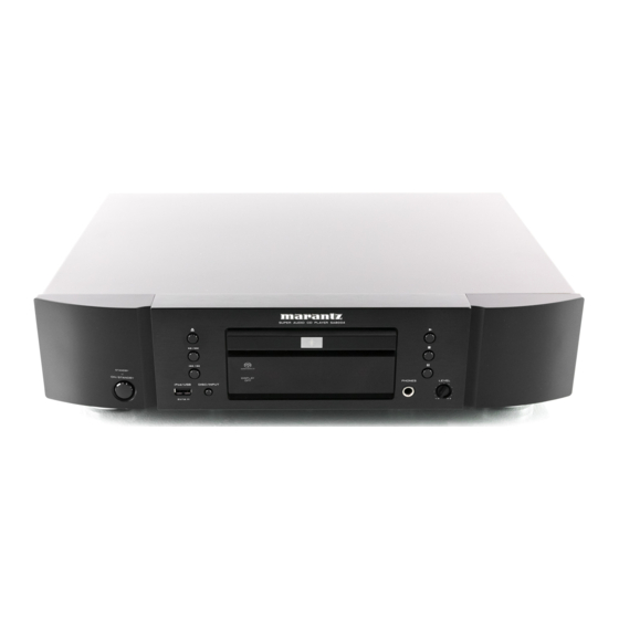
SA8004
SA-KI-PEARL-LITE
Copyright 2010 D&M Holdings Inc. All rights reserved.
WARNING: Violators will be prosecuted to the maximum extent possible.
SA8004 /
SA-KI-PEARL-LITE /
Super Audio CD player
K1SG/U1B
N1SG/N1B
Ver. 2
Please refer to the
MODIFICATION NOTICE.
Advertisement
Table of Contents

Related Manuals for Marantz SA8004/K1SG


Summary of Contents for Marantz SA8004/K1SG
- Page 1 Service SA8004 / K1SG/U1B SA-KI-PEARL-LITE / N1SG/N1B Manual Super Audio CD player • For purposes of improvement, specifi cations and design are subject to change without notice. • Please use this service manual with referring to the operating instructions without fail. •...
-
Page 2: Ordering Parts
MARANTZ Parts for your equipment are generally available to our National Marantz Subsidiary or Agent. ORDERING PARTS : Parts can be ordered either by mail or by Fax.. In both cases, the correct part number has to be specifi ed. -
Page 3: Safety Precautions
SAFETY PRECAUTIONS The following check should be performed for the continued protection of the customer and service technician. LEAKAGE CURRENT CHECK Before returning the unit to the customer, make sure you make either (1) a leakage current check or (2) a line to chassis resistance check. -
Page 4: Note For Schematic Diagram
NOTE FOR SCHEMATIC DIAGRAM WARNING: Parts marked with this symbol z have critical characteristics. Use ONLY replacement parts recommended by the manufacture CAUTION: Before returning the unit to the customer, make sure you make either (1) a leakage current check or (2) a line to chassis resistance check. If the leakage current exceeds 0.5 milliamps, or if the resistance from chassis to either side of the power cord is less than 460 kohms, the unit is defective. -
Page 5: Warning And Laser Safety Instructions
WARNING AND LASER SAFETY INSTRUCTIONS WARNING WAARSCHUWING All ICs and many other semi-conductors are Alle IC’s en vele andere halfgeleiders zijn susceptible to electrostatic discharges (ESD). gevoelig voor elektrostatische ontladingen Careless handling during repair can reduce (ESD). life drastically. Onzorgvuldig behandelen tijdens reparatie When repairing, make sure that you are kan de levensduur drastisch doen connected with the same potential as the... -
Page 6: Instructions For Handling Semi-Conductors And Optical Unit
INSTRUCTIONS FOR HANDLING SEMI-CONDUCTORS AND OPTICAL UNIT Electrostatic breakdown of the semi-conductors or optical pickup may occur due to a potential difference caused by electrostatic charge during unpacking or repair work. 1. Ground for Human Body Be sure to wear a grounding band (1 MΩ) that is properly grounded to remove any static electricity that may be charged on the body. -
Page 7: Technical Specifications
TECHNICAL SPECIFICATIONS n Audio performance [Super Audio CD] [CD] • Analog output Channels: 2 channels 2 channels Playable frequency range: 2 Hz – 100 kHz 2 Hz – 20 kHz Playable frequency response: 2 Hz – 50 kHz (–3 dB) 2 Hz –... -
Page 8: Caution In Servicing
Refer to "MEASURING METHOD AND WAVEFORMS". Service Jigs When you update the fi rmware, you can use the following Please order to marantz Offi cial Service Distributor in your region if necessary. 8U-210100S : WRITING KIT : 1 Set... - Page 9 DISASSEMBLY • Disassemble in order of the arrow of the fi gure of following fl ow. • In the case of the re-assembling, assemble it in order of the reverse of the following fl ow. • In the case of the re-assembling, observe "attention of assembling" it. •...
-
Page 10: Front Panel Assy
1. FRONT PANEL ASSY Proceeding : TOP COVER LOADER PANEL FRONT PANEL ASSY → → (1) Detach the DOOR. Direction of photograph: B (2) Remove the screws. (3) Disconnect the connector wires and FFC cables, then remove the screws. N502 N401 FFC cable Please refer to "EXPLODED VIEW"... -
Page 11: Dac/Audio Pwb
2. DAC/AUDIO PWB Proceeding : TOP COVER DAC/AUDIO PWB → (1) Remove the screws. Direction of photograph: A (2) Disconnect the connector wires and FFCs cable, then remove the screws. N401 PWB Clamper FFC Cable N201 N851 DAC/AUDIO PWB N302 N301... -
Page 12: Dir/Usb-Dac Pwb
3. DIR/USB-DAC PWB Proceeding : TOP COVER DIR/USB-DAC PWB → (1) Remove the screws. Direction of photograph: A (2) Disconnect the FFC cable. PWB Clamper FFC Cable DIR/USB-DAC PWB... -
Page 13: Power/Ucom/Usb Pwb
4. POWER/uCOM/USB PWB Proceeding : TOP COVER POWER/uCOM/USB PWB → (1) Remove the screws. Direction of photograph: A (2) Disconnect the connector wires and FFC cables, then remove the screws. FFC Cable FFC Cable N502 N181 N182 POWER/uCOM PWB Clamper /USB PWB N251 N803... -
Page 14: Mecha Assy
5. MECHA ASSY Proceeding : TOP COVER LOADER PANEL MECHA ASSY → → (1) Remove the screws. (2) Disconnect the connector wires and FFC cables. FFC Cable FFC Cable N181 N182... -
Page 15: Cautions In Assembling And Disassembling
CAUTIONS IN ASSEMBLING AND DISASSEMBLING When removing the FFC (fl exible fl at cable), connecting the optical pick up and the Super Audio CD PWB, short the short three lands pointed by the arrow with solder. Otherwise the laser diode may be damaged by static electricity ※... -
Page 16: Removing Discs
REMOVING DISCS (1) Remove the Top Cover. (2) Remove the screws. (3) Remove the disc clamper. (3) Now you can remove the disc. -
Page 17: Service Mode
SERVICE MODE (1) Insert mains cable plug in the outlet. (The Unit is standby mode.) (2) Press the ON/STANDBY button While pressing 7 / 9 and 2 button. Model name is displayed. SA8004 (3) Press 7 / 9 button Press 6 / 8 button Version of FRONT microprocessor is displayed. - Page 18 Serial number is displayed. MZ_XXXXXXXXX (11) Press 7 / 9 button Press 6 / 8 button [A] SA-CD payback time is displayed. [B] SA-CD backup time is displayed. Press 1 button PTime : 00021h PTime : 00021h Press 3 button (12) Press 7 / 9 button Press 6 / 8 button [A] CD payback time is displayed.
-
Page 19: How To The Reset Of Playback Time
HOW TO THE RESET OF PLAYBACK TIME When replacing CD MECHANISM [ 001M or M002 ] (TRAVERSE Block), please reset Playback time (total) in the following procedure. (1) Procedure 11, 12 of SERVICE MODE, Playback time (total) is displayed. PTime : 10051h The display is a time unit. -
Page 20: Error Message
ERROR MESSAGE This test mode is common to all models. [A] The mode to check the last error message etc. “ 2 ” + “ 7 / 9 ” + “ON/STANDBY” Model name displayed SA8004 STOP Previous 8 / 6 STOP(3s) Clear Last Error Massage... - Page 21 2. Error Rate This function determines the CD error rate. For SA-CDs, it only displays reference values. A- B 1 RNDM PROG SA-CD M FILE STRG D OFF REMAIN TTL Display E r r o a t e _ _ _ The buttons that function while this message is being displayed are 5 and 1 .
- Page 22 4. Tray Speed Test This function allows the OPEN/CLOSE speed of the tray to be variable. It can be changed at a 1% step to the default values. Here are default values: Time 0-500ms 500ms-1s 1s-1.5s 1.5s-2s 2s~ TRY_OPN 85 % 65 % 55 % 55 %...
- Page 23 [B] The mode to check the last error message etc. This test mode is common to all models. 1. The error message displayed as the Last Error Message (1) Communication error between SA-CD Module and Microprocessor When having had the communication error with the SA-CD Module more than a regulated number of times, the unit will reset the SA-CD Module after displaying the following message.
- Page 24 [C] Error Messages special to USB 1. Error Message displayed as the Last Error Message If no response is made in the communication between the USB Module U501 and the microprocessor within a designated timeframe, the display will show the following message. Refer to the Communication between USB Module and the microprocessor on the Communication Waveform page and check the signal.
- Page 25 2. Error Message not displayed as the Last Error Message (1) Error Message that is displayed when UBS memories and USB HDD are used If no response is made while the unit is communicating with the USB Module, the display will show the following message.
- Page 26 If no playable fi le exists in the USB device connected to the unit, the display will show the following message: A- B 1 RNDM PROG SA-CD M FILE STRG D OFF REMAIN TTL Display i l e r r _ If the unit receives a power supply exceeding the maximum level (1 A) via USB, the display will show the following message and the power supply will be cut off.
- Page 27 If the unit detects a fi le with corrupted fi le data or other unacceptable fi les, the display will show the following message. A- B 1 RNDM PROG SA-CD M FILE STRG D OFF REMAIN TTL Display S t r E r r If the fi...
- Page 28 If the unit has failed to obtain information of the fi le to be played back, the display will show the following message. If this error occurs to a specifi c fi le, the fi le information may be corrupted. Check the fi le header and other information.
- Page 29 (2) Error Message that can be displayed while an iPod device is connected If the unit experiences an error in the recognition process or fails to receive required information from an iPod device, the display will show the following message. If this error has occurred, try unplugging and plugging the device again.
- Page 30 If an error occurs to communication commands while the unit is performing normal operations including PLAY, PAUSE and SEARCH, the display will show the following message. This message is mainly for debugging software and normally does not appear. After this message is displayed, the unit automatically resets the USB module. If the error persists after the unit is restarted, U501 may be broken as it will not accept a specifi...
-
Page 31: Version Upgrade Procedure Of Firmware
VERSION UPGRADE PROCEDURE OF FIRMWARE ABOUT REPLACE THE MICROPROCESSOR WITH A NEW ONE When replaced of the U-PRO (Microprocessor), confi rm contents of the following. After PWB Name Ref. No. Description Remark replaced 8U-210103-1 U102 R5F212CCSNFP After replaced A : Mask ROM (With software). No need write-in of software to the microprocessor. B : Flash ROM (With software). - Page 32 (3) Connect FPC (upside contact) to the rear panel of the unit from DATA UPDATE KIT (4) Connect the mains cord into the unit. (5) Double click the FlashSta.exe. And launch the M16 Flash Start. 8004 8004 8004...
- Page 33 (6) Check the Internal fl ash memory in the Select Program. Choose the COM Port number. And click the OK. (7) Click the Refer..
- Page 34 (8) Choose the SACD_yymmdd.mot. And click the Open. NOTE : The yy is two digits of year. The mm is month. The dd is date. 8004 (9) The FilePath and ID are inputted automatically, and the MCU Type is selected to R8C automatically. Click the OK.
- Page 35 (10) Click the E.P.R..(11) Click the OK.
- Page 36 (12) Software is written into the internal Flash-ROM of Front CPU. The writing of software takes about 1 minute. (13) Click the OK. (14) Click the Exit. (15) Disconnect the mains cord. (16) Disconnect the FFC of DATA UPDATE KIT from the unit.
-
Page 37: [B] Update Firmware For Super Audio Cd Module
[B] UPDATE FIRMWARE FOR Super Audio CD MODULE Necessary Equipment • Update Disc (90M-SA7003CDR) WRITING PROCEDURE (1) Connect the mains cord into the unit. (2) Turn on the unit. (3) Press the 5 button to open the tray. (4) Insert the Update Disc. (5) Press the 5 button to close the tray. -
Page 38: Troubleshooting
TROUBLE SHOOTING b Please refer to "MEASURING METHOD AND WAVEFORMS" for details in a waveform. 8U-210103-1(DIGITAL POWER UNIT) Check the DIGITAL power supply component Check soldering and replace FUSE. Check Power Supply-1 N.G. ・D883,D884,D885,D886 8U-210103-1(DIGITAL POWER UNIT) ・U881 ・Check FUSE (F801) ・STANDBY TRANS(T881) O.K. - Page 39 00MZK35AK0020(SACD MODULE UNIT) Check the voltage of SACD module Check Power Supply-1 8U- 210103-1 Check the cable and the connection of connector. ・Check the output voltage of N103 29 pin : +12V N.G. Check soldering. ・Check the output voltage of N103 28 pin : +8V ・N103 ・Check the output voltage of N103...
- Page 40 8U-210103-2(AUDIO UNIT) Check AUDIO UNIT Check the cable and the connection of connector. Check the Power Supply-1 Check soldering. N.G. 8U-210103-2(AUDIO UNIT) ・N851 ・Check the output voltage of Q853 +12V ・D851,D852,D853,D854 ・Check the output voltage of Q854 -12V Check FUSE. ・F851,F852 O.K.
- Page 41 Check analog output-1 N.G. Check soldering. 8U-210103-2(AUDIO UNIT) ・C,R around U204 ・U204 (23)(24)(19)(20)pin : Analog output O.K. Check analog output-2 N.G. Check soldering. 8U-210103-2(AUDIO UNIT) ・Q323,Q325,Q324,Q326 ・Check analog output O.K. Check mute signal Check the cable and the connection of connector. 8U-210103-2(AUDIO UNIT) N.G.
- Page 42 8U-210103-3(DIR,USB_DAC UNIT) Check the Power Supply-1 Check the cable and the connection of connector. N.G. 8U-210103-3 Check soldering. ・Check the voltage of N631 2pin : 3.3V ・N601 O.K. Check signal of U634 (DIR) 8U-210103-3 41pin : Is DIR_RES ”H”? ・U634 ・Check starting oscilltor U634 28pin...
- Page 43 8U-210103-1(USB_iPod) Check the cable and the connection of connector. Check power supply Check soldering. N.G. 8U-210103-1 ・U811 (8U-210103-1) ・Check voltage of U501 ・N104 (8U-210103-1) (6)(13)(48)(53)(62)(96)(116)(128)(143)pin : 3.3V ・U701 (8U-110090-1) ・N701 (8U-110090-1) O.K. Check signal of U501 (FRONT USB/iPod) 8U-210103-1 19pin : Is USB_RES ”H”? ・U501 ・Check starting oscilltor.
-
Page 44: Measuring Method And Waveforms
MEASURING METHOD AND WAVEFORMS To check the waveforms on the Main P.W.B., the GND (-) probe of the oscilloscope to “Vref” point.(Except for lnner SW, TRVSW) Measuring Disc: SACD/DAC Test Disc CD/TCD-784 (It is better to use wires for extending between the probe and test points.) •... - Page 45 WAVEFORMS DIR, USB_DAC UNIT SACD MODULE UNIT t DIR_CL q ACK r XREDY y DIR_CE u DIR_DI w MDATA e MDATA i DIR_DO FRONT UNIT Q2 DIR_MCLK W3 DIS_SO Q1 DIR_SCLK W4 DIS_SCL o DIR_DATA W5 DIS_CS Q0 DIR_LRCK Q3 D+ AUDIO UNIT PCM mode Q4 D-...
- Page 46 Personal notes:...
-
Page 47: Block Diagram
BLOCK DIAGRAM RC-5 from EXT CONTROL MPU FRONT PANEL RC-5 (Display off) (RC-5) (IN) 11pin(SDA) Display KEYS 10pin(SCL) COAX 13pin(RST) HDAM LPF PLAY, STOP, PAUSE, NEXT, BACK, DIS_SO,DIS_SCL_DIS_ L. OUT KEYES OPEN/CLOSE,DISC/INPUT and AMP CS_DIS_RESET Model 12pin(CS1) select 9pin(CS2) to phones Vol MODE CS4398 Muting... -
Page 48: Wiring Diagram
WIRING DIAGRAM N702 FRONT UNIT 8U-110090-1 Super Audio CD N701 N751 STANDBY SW UNIT 8U-110090-2 N451 HEADPHONE UNIT N551 N552 FRONT USB UNIT 8U-110090-3 8U-110090-4 CORE CORE SA-CD LOADER MECHANISM N401 N203 CN95 CN10 N104 N501 N502 CORE N103 N181 SA-CD SURVO UNIT N601 N182... -
Page 49: Printed Wiring Boards
PRINTED WIRING BOARDS FRONT (COMPONENT SIDE) JV12 PLAY OP/CL S722 S721 JV15 STOP NEXT S724 S723 B701 8U-110090-1 631010090107M JV28 C712 JV29 15.0 FRONT UNIT J742 PREVIOUS PAUSE JV27 S725 S726 12.5 D701 Z702 DISC/USB S727 Z701 C705 C710 JV33 JV34 17.5 FRONT (FOIL SIDE) - Page 50 HEAD PHONE (COMPONENT SIDE) POWER SW (COMPONENT SIDE) FRONT USB (COMPONENT SIDE) N751 B552 N552 K451 D751 N551 B451 Z751 8U-110090-4 B551 FRONT USB UNIT JV25 C553 V451 S751 JV21 K551 N451 FRONT USB (FOIL SIDE) HEAD PHONE (FOIL SIDE) POWER SW (FOIL SIDE) L451 R753...
- Page 51 DAC/AUDIO (COMPONENT SIDE) DIR/USB-DAC (COMPONENT SIDE) B302 S901 K901 N301 N302 K302 K301 8U-210103-2 C665 Q854 R691 C901 DAC/AUDIO D632 C643 D633 C632 R357 R358 R356 R355 C661 U632 C333 C334 Q481 R486 C634 D481 D482 Q484 Q482 R481 R482 R852 C662 R668...
- Page 52 DAC/AUDIO (FOIL SIDE) DIR/USB-DAC (FOIL SIDE) R901 C902 C677 C682 D901 D634 R694 R701 R220 R227 C205 R217 R218 R219 R201 R210 R221 R224 R209 R222 R208 R223 R207 R206 R205 R204 R203 C403 C201 C202 C404 鉛フリー半田 半田付けには、鉛フリー半田 (Sn-Ag-Cu) を使用してください。 Lead-free Solder When soldering, use the Lead-free Solder (Sn-Ag-Cu).
- Page 53 POWER/UCOM/USB (COMPONENT SIDE) N941 K921 8U-210103-1 K922 G VCC B941 C922 632010103204M C929 C927 R925 R926 POWER/uCOM/USB C930 L922 R832 D833 D832 C923 U921 R924 C926 C921 R921 R922 C924 C925 D451 D452 Q832 R833 C802 F802 D824 D822 T1.25AL 250V F801 D823 N801...
- Page 54 POWER/UCOM/USB (FOIL SIDE) C931 C932 C928 L921 Q833 R836 R835 Pri. L811 Sec. R811 L821 R110 R108 R111 L823 L822 R455 L602 L601 Q453 R452 D453 R451 R460 D455 R456 C889 R457 C892 R106 R137 Q186 Q103 R118 Q101 R131 R132 R130 R129...
-
Page 55: Schematic Diagrams
R1021 R1031 R602 OPEN DIR_MCLK DIR_MCLK 5101 UCOM 8U-D41251010 FRONT R1022 R1032 R603 DIR_SCLK DIR_SCLK OPEN R604 DIR_LRCK R1023 R1033 FL POWER DIR_LRLK OPEN MAX.153m A R605 DIR_DATA DIR_DATA TYP.140m A R606 AC3.3V DIR_RES DIR_RES GNDM GNDST GNDM GNDD R843 AC3.3V R608 To/From... - Page 56 & OUTPUT PCB(PP16) 00MWGD1421030 N205 B302 V+11A1 5103 8U-BD210103 M3-SIDE V+3.3D1 7P-FFC R339 R305 D301 D309 1SS133 C325 1SS133 R301 Q319 220/25 D311 N203 L202 D303 R307 1SS133 EARTH BLM21PG221 R317 1SS133 2SA1015 17P-FFC GND1 GND1 4.7K GND1 GNDD Q315 R341 R203 0 V+3.3D1...
- Page 57 Z103 STYLE-PIN UART_TXD UART_RXD DATE GNDM DOWNLOAD_SW N103 L101 USB_SO 29P-FFC L102 USB_SI L103 USB_SCK 1 TEST(NC) L104 USB_CTS 2 (NC) L105 USB_DDI 3 (NC) L106 USB_NMI 4 (NC) L107 USB_STBY_B 5 SPDIF_RQ L108 USB_RTS 6 (NC) GNDM GNDST R103 IPOD_ERR 7 DVDMUTE R104...
- Page 58 N631 25P-FFCs V+3.3VR DIR_MCLK. DTR_MCLK DIR_SCLK. DIR_SCLK GNDD5 DIR_LRCK. GNDD5 DIR_LRCK R675 GNDD5 V+3.3VR DIR_DATA. DIR_DATA DIR_RES. DIR_RES DIR RECEIVER GNDD5 DIR_CL. DIR_CL R681 10K C676 DIR_CE. R650 DIR_CE RXOUT RERR V+3.3VR R651 R679 DIR_DI. DIR_DI R652 R682 DIR_DO. CKST DIR_DO R653 R683...
- Page 59 N501 6P-FFC 00MWGD4122000 PP16 GNDU R516 GNDU R517 R509 V+3.3DD GNDM GNDU USB_SI GNDU V+5DU USB_SI Z501 BLM21PG221 USB_SO nanoSMDC110F L501 USB_SO GNDM GNDM USB_SCK USB_SCK USB_CTS GNDM GNDM R515 USB_CTS GNDM USB_DDI GNDM N502 USB_DDI GNDM USB_NMI 3P-PH V+3.3DD USB_NMI X502 USB_STBY_B...
- Page 60 RU S PH26 00MWGA1422020 PF16 00MWGA1422010 PP26 00MWGA1422040 FRONT USB PCB(PP26) FRONT PCB (PF16) POWER SW PCB(PH26) B701 8U-110090- B701 1P-WIRE 8U-110090- 8U-110090-2 N552 Z703 Z704 3P-PHs K551 Z751 FL_HOLDER FL_HOLDER STYLE-PIN USB_CONNECTOR EARTH 454310003006 454310003006M VBUS GNDM GNDM 4P-PHs 4P-PHs E+3.3V.
-
Page 61: Exploded View
EXPLODED VIEW W0001 5129 5146 Ø3X8(M) Ø3X8(M) 5129 Ø3X8(M) 0073G 5126 5110 K0001 5148 Ø3X8(M)x2 Ø3X8(M) Ø3X6(M) 5128 5127 Ø3X8(M)x3 Ø3X8(M) 5110 5127 Ø3X6(M) L0003 Ø3X8(M)x5 5146 T0881 Ø3X6(M)x3 K0303 K0304 5128 DIR/ Ø3X8(M) USB-DAC PWB M0901 0003D 0071Gx2 5126 0001D Ø3X8(M) 5110... - Page 62 00MTS56903030 !TROIDAL TRANS AC230V (N) 0003B 402410114058M FRONT PANEL SA-KI-PEARL-LITE BL L0001 00MTS56903030 !TROIDAL TRANS AC230V (N) 0005B 421410006004M MARANTZ BADGE (AL) FOR M1 MODEL L0001 00MTS56903020 !TROIDAL TRANS AC120V (U) 0011B 443510004038M CHASSIS SG SA7003 33AK L0003 TFCK-23-11-14 0011B...
-
Page 63: Exploded View Of Cd Mechanism Unit
EXPLODED VIEW OF CD MECHANISM UNIT Ref. No. Part No. Part Name Remarks Q'ty ★ 15 606050039005S FFC CABLE 24PIN 0.5MM PITCH L=11CM W1001<->CN101 ★ 16 CONT.LABEL BASE(D&M) 0001S ★ 17 CONT LABEL FILM 0002S ★ 18 SHEET SA7003 33AK 0081G ★... -
Page 64: Packing View
PACKING VIEW Ref. No. Part No. Part Name Remarks Q'ty 0055T POLY COVER 0013S 0061T WARRANTY USA 0021T 0071T WARRANTY CANADA W0001 00D2062249001 AC CORD (E1C) 0003S 0031T W0001 00MZC01803080 # 2P AC CORD 10A 250V CLASS2 W0082 W0001 00MZC01803100 # AC CORD UL/CSA 10A 125V 0005T W0001... - Page 65 SEMICONDUCTORS Only major semiconductors are shown, general semiconductors etc. are omitted to list. The semiconductor which described a detailed drawing in a schematic diagram are omitted to list. 1. IC's LC89057W-VF4 (MAIN :U634) 35 34 33 32 31 30 29 28 27 26 25 SDIN SLRCK SBCK...
- Page 66 LC89057W-VF4 Terminal Functions Pin No. Name Function RXOUT Output pin of Input bi-phase selection data Input pin of TTL-compatible digital data Digital data input pin with built-in amplifier that supports coaxial Input pin of TTL-compatible digital data Input pin of TTL-compatible digital data DGND Digital GND DV DD...
- Page 67 (MAIN : U204) CS4398 120 dB, 192 kHz Multi-Bit DAC with Volume Control Features Advanced Multi-bit Delta-Sigma Architecture Direct Stream Digital (DSD) – 120 dB Dynamic Range – Dedicated DSD Input Pins – -107 dB THD+N – On-Chip 50 kHz Filter to Meet Scarlet Book SACD Recommendations –...
- Page 68 CS4398 (MAIN : U204) DSD_B DSD_A DSD_SCLK SDIN SCLK AMUTEC LRCK AOUTA- MCLK AOUTA+ DGND AGND M3 (AD1/CDIN) AOUTB+ M2 (SCL/CCLK) AOUTB- M1 (SDA/CDOUT) BMUTEC M0 (AD0/CS) VREF REF_GND FILT+ CS4398 Terminal Functions Pin Name Pin # Pin Description DSD_A Direct Stream Digital Input (Input) - Input for Direct Stream Digital serial audio data.
-
Page 69: Top View
R5F212CCSNFP (MAIN :U102) 60 59 58 57 56 55 54 53 52 51 50 49 48 47 46 45 44 43 42 41 P7_4/AN16 P8_2/TRFO02 P7_3/AN15 P8_3/TRFO10/TRFI P7_2/AN14 P8_4/TRFO11 P7_1/AN13 P8_5/TRFO12 P7_0/AN12 P8_6 P0_0/AN7 P8_7 P0_1/AN6 P1_4/TXD0 P0_2/AN5 P1_5/RXD0/(TRAIO)/(INT1) P0_3/AN4 P1_6/CLK0 R8C/2C Group P0_4/AN3... - Page 70 R5F212CCSNFP Block diagram I/O ports Port P0 Port P1 Port P2 Port P3 Port P4 Port P5 Peripheral functions UART or System clock generation clock synchronous serial I/O circuit Timers (8 bits XIN-XOUT Timer RA (8 bits High-speed on-chip oscillator Timer RB (8 bits C bus or SSU Low-speed on-chip oscillator...
- Page 71 PORT NAME INITIAL FUNCTION STBY TRCIOC TRY_CLS TRAY CLOSE OUTPUT PWM OUTPUT P5_2 DIR_XMODE DIR RESET OUTPUT P5_1 DAC_GAIN DAC GAIN CHANGE OUTPUT P5_0 INVERT_LED BALANCE OUTPUT POLARITY DISPLAY LED P9_3 SUSPEND USB DAC ENABLE SIGNAL P9_2 STB_LED STANDBY LED OUTPUT P9_1 P9_0 P2_7...
- Page 72 PORT NAME INITIAL FUNCTION STBY KEY_1 KEY INPUT AD INPUT KEY_2 KEY INPUT AD INPUT KEY_3 KEY INPUT AD INPUT TRAY_IN_SW TRAY OPEN CLOSING TRIGGER INPUT AD INPUT P0_4 DIR_DO DIR IC DATA OUTPUT P6_2 DIR_DI DIR IC DATA INPUT P6_1 DIR_CL DIR IC CLOCK OUTPUT...
- Page 73 EPM3032A Terminal Functions Pin Name Name/Usage Pin No. Dir. I/O Standard Voltage User Assignment input 3.3-V LVTTL N For PLD writing SEL2 RESERVED_INPUT RESERVED_INPUT GNDIO SYCL SMLCK output 3.3-V LVTTL Y Master Clock output LRCK/SAR SWCLK output 3.3-V LVTTL Y Word Clock output input 3.3-V LVTTL N For PLD writing...
- Page 74 TE7022L (MAIN :U632) TE7022L Pin Descriptions...
- Page 75 TE7022L Pin Descriptions...
- Page 76 uPD63901GJ (MAIN :U501) 144 143 142 141 140 139 138 137 136 135 134 133 132 131 130 129 128 127 126 125 124 123 122 121 120 119 118 117 116 115 114 113 112 111 110 109 USBXTAL RA11 USBXTAL RA10...
- Page 77 Pin No. Pin Name Pin Description Initial Standby RESET Control Engine Reset Standby signal output High-Z Standby signal input High-Z INTP1 Command RTS input High-Z N.C. BIN_STB Download strobe input High-Z BIN_SO Download Data input High-Z BIN_CLK Download Clock High-Z N.C.
-
Page 78: Dram Clock
Pin No. Pin Name Pin Description Initial Standby TEST1 Test port TEST2 Test port TEST3 Test port C33M DRAM CLOCK N.C. N.C. DRAM RAS output CAS0 DRAM Lower CAS output CAS1 DRAM Upper CAS output DRAM WE output DRAM OE output RDB0 DRAM Data0 input High-Z... - Page 79 Pin No. Pin Name Pin Description Initial Standby N.C. N.C. N.C. N.C. N.C. N.C. N.C. A.GND Analog GND Analog VDD N.C. N.C. N.C. N.C. N.C. N.C. N.C. N.C. N.C. N.C. N.C. N.C. N.C. N.C. Analog VDD A.GND Analog GND...
-
Page 80: Pin Connection
2. FL DISPLAY FLD (13-BT-237INK) (FRONT : Z0701) PIN CONNECTION GRID ASSIGNMENT... - Page 81 ANODE CONNECTION...
-
Page 82: Parts List Of P.w.b. Unit
PARTS LIST OF P.W.B. UNIT zParts for which "nsp" is indicated on this table cannot be supplied. zThe parts listed below are for maintenance only, might differ from the parts used in the unit in appearances or dimensions. Note: The symbols in the column "Remarks" indicate the following destinations. U : North America model N : Europe model K : China model... - Page 83 Ref. No. Part No. Part Name Remarks Q'ty C0714 00D2570507976 CC73CH1H331JT +1608 C0715,0716 C1608X7R1H104K (0.1UF 50V) C0718,0719 C1608X7R1H104K (0.1UF 50V) C0720,0721 00D2544299964 CE04W1C470MT(SRE) C0751,0752 C1608X7R1H104K (0.1UF 50V) OTHERS PARTS GROUP L0451,0452 RM73B--0R0KT +1608 N0451 B8B-PH-K-S (LF)(SN) N0551 6P FFC BASE(9610SA) N0552 S3B-PH-K-S (LF)(SN) N0701...
-
Page 84: Main Pwb Assy
MAIN PWB ASSY Ref. No. Part No. Part Name Remarks Q'ty SEMICONDUCTORS GROUP D0301-0316 00D2760401905 1SS133T77 (TAPE) D0401-0404 00D2760401905 1SS133T77 (TAPE) z D0451,0452 00D2760704903 1SR35-400A(T93X) D0453 00MHZ3047100Y MA8047-M 4.7V z D0454 00D2760704903 1SR35-400A(T93X) D0455 00D2760794900 KDS160-RTK/P D0456 00D2760704903 1SR35-400A(T93X) D0457,0458 00D2760794900 KDS160-RTK/P D0481,0482... - Page 85 Ref. No. Part No. Part Name Remarks Q'ty U0204 00MHC10020880 CS4398-CZZR/D U0401 00MHC10111090 DUAL LOW NOISE OP-AMP NJM2114D U0501 239810050604S UPD63901-501 U0601 00D2623447909 TC4053BFT U0632 239810048601S TE7022L U0633 U0634 00D2623449004 LC89057W-VF4A U0636 00MHC10433990 AT24C08BN-SH-T U0637 236810074502S CS2100**-CZZR z U0811 00MHC3190532F !PQ05RD21 5V 2A z U0821 00D2630810008 NJM7808FA(S)
- Page 86 Ref. No. Part No. Part Name Remarks Q'ty Q0326 00D2710102924 2SA1015(GR)TPE2 Q0401 00D2730198921 2SC1815(GR)TPE2 Q0402 00D2730198921 2SC1815(GR)TPE2 Q0403 00D2710102924 2SA1015(GR)TPE2 Q0404 00D2710102924 2SA1015(GR)TPE2 Q0451 00D2730198921 2SC1815(GR)TPE2 Q0452 00D2730198921 2SC1815(GR)TPE2 Q0453 00D2690088906 DTC114TKT96 Q0454 00D2690088906 DTC114TKT96 Q0456 00D2710102924 2SA1015(GR)TPE2 Q0457 00D2690088906 DTC114TKT96 Q0481 00D2730460905...
- Page 87 Ref. No. Part No. Part Name Remarks Q'ty R0118 RM73B--103JT +1608 R0119 RM73B--103JT +1608 R0120 RM73B--103JT +1608 R0121 RM73B--0R0KT +1608 R0122 RM73B--103JT +1608 R0123 RM73B--220JT +1608 R0124 RM73B--104JT +1608 R0125 RM73B--220JT +1608 R0126 RM73B--104JT +1608 R0127 RM73B--102JT +1608 R0128 RM73B--222JT +1608 R0131 RM73B--222JT...
- Page 88 Ref. No. Part No. Part Name Remarks Q'ty R0222 RM73B--470JT +1608 R0223 RM73B--470JT +1608 R0224 RM73B--470JT +1608 R0225 RM73B--103JT +1608 R0226 RM73B--103JT +1608 R0227 RM73B--223JT +1608 R0347 00MGG05100160 10 OHM +- 5% 1/6W FLAMERETARDANT R0348 00MGG05100160 10 OHM +- 5% 1/6W FLAMERETARDANT R0349 00MGG05100160 10 OHM +- 5% 1/6W FLAMERETARDANT R0350...
- Page 89 Ref. No. Part No. Part Name Remarks Q'ty R0525 RM73B--103JT +1608 R0601 RM73B--220JT +1608 R0602 RM73B--220JT +1608 R0603 RM73B--220JT +1608 R0604 RM73B--220JT +1608 R0605 RM73B--220JT +1608 R0606 RM73B--220JT +1608 R0608 RM73B--220JT +1608 R0609 RM73B--220JT +1608 R0610 RM73B--220JT +1608 R0611 RM73B--220JT +1608 R0612 RM73B--220JT...
- Page 90 Ref. No. Part No. Part Name Remarks Q'ty R0670 RM73B--101JT +1608 R0671 RM73B--101JT +1608 R0672 RM73B--223JT +1608 R0673 RM73B--103JT +1608 R0674 RM73B--103JT +1608 R0675 RM73B--103JT +1608 R0676 RM73B--103JT +1608 R0677 RM73B--103JT +1608 R0678 RM73B--221JT +1608 R0679 RM73B--101JT +1608 R0680 RM73B--105JT +1608 R0681 RM73B--103JT...
- Page 91 Ref. No. Part No. Part Name Remarks Q'ty R0887 RM73B--103JT +1608 R0888 RM73B--153JT +1608 R0901 RM73B--470JT +1608 R0921 RM73B--122JT +1608 R0922 RM73B--332JT +1608 R0924 RM73B--330JT +1608 R0925 RM73B--391JT +1608 R0926 RM73B--102JT +1608 R0927 RM73B--750JT +1608 R0981 RM73B--0R0KT +1608 R0982 RM73B--0R0KT +1608 R0983 RM73B--0R0KT...
- Page 92 Ref. No. Part No. Part Name Remarks Q'ty C0205 C1608X7R1H104K (0.1UF 50V) C0206 C1608X7R1H104K (0.1UF 50V) C0207 C1608X7R1H104K (0.1UF 50V) C0208 C1608X7R1H104K (0.1UF 50V) C0209 C1608X7R1H104K (0.1UF 50V) C0210 00MOA107025Z1 ROS-25V 101M - H4#PE - T2 (100UF 25V) C0211 C1608X7R1H104K (0.1UF 50V) C0212 00MOA107025Z1 ROS-25V 101M - H4#PE - T2 (100UF 25V) C0213...
- Page 93 Ref. No. Part No. Part Name Remarks Q'ty C0451 00D2544586978 CE04W2A010MT(RA3) C0452 00D2544814019 CE04W1E102MC(KMG) C0453 00D2544586936 CE04W2A4R7MT(RA3) C0501 00D2570503967 CC73CH1H150JT +1608 C0502 00D2570503967 CC73CH1H150JT +1608 C0503 00MDK96104300 C1608X7R1H104K (0.1UF 50V) C0504 00D2544569911 CE04W1E470MT(RA3) C0505 C1608X7R1H104K (0.1UF 50V) C0506 C1608X7R1H104K (0.1UF 50V) C0507 00D2544569911 CE04W1E470MT(RA3)
- Page 94 Ref. No. Part No. Part Name Remarks Q'ty C0656 C1608X7R1H104K (0.1UF 50V) C0657 C1608X7R1H104K (0.1UF 50V) C0658 C1608X7R1H104K (0.1UF 50V) C0659 C1608X7R1H104K (0.1UF 50V) C0660 C1608X7R1H104K (0.1UF 50V) C0661 00D2544569911 CE04W1E470MT(RA3) C0662 00D2544569911 CE04W1E470MT(RA3) C0663 C1608X7R1H104K (0.1UF 50V) C0666 00D2570503912 CC73CH1H9R0DT +1608 C0667...
- Page 95 Ref. No. Part No. Part Name Remarks Q'ty C0886 CK73B1H102KT +1608 C0887 00D2544802908 CE04W1J101MT(RA3) C0888 C1608X7R1H104K (0.1UF 50V) C0889 C1608X7R1H104K (0.1UF 50V) C0890 00D2544577945 CE04W1C101MT(RA3) C0891 00D2544586978 CE04W2A010MT(RA3) C0892 C1608X7R1H104K (0.1UF 50V) C0893 00D2544577945 CE04W1C101MT(RA3) C0901 133050074586S CQ93M2E471J(LP) C0902 C1608X7R1H104K (0.1UF 50V) C0903 C1608X7R1H104K (0.1UF 50V) C0921...
- Page 96 Ref. No. Part No. Part Name Remarks Q'ty L0203 E.FIL(BLM21PG221SN1)+2125 L0251 E.FIL(BLM21PG221SN1)+2125 L0451 E.FIL(BLM21PG221SN1)+2125 L0501 E.FIL(BLM21PG221SN1)+2125 L0502 E.FIL(BLM21PG221SN1)+2125 L0601 E.FIL(BLM21PG221SN1)+2125 L0602 E.FIL(BLM21PG221SN1)+2125 L0632 E.FIL(BLM21PG221SN1)+2125 L0633 E.FIL(BLM21PG221SN1)+2125 L0811 E.FIL(BLM21PG221SN1)+2125 L0821 E.FIL(BLM21PG221SN1)+2125 L0822 E.FIL(BLM21PG221SN1)+2125 L0823 E.FIL(BLM21PG221SN1)+2125 L0831 E.FIL(BLM21PG221SN1)+2125 L0841 E.FIL(BLM21PG221SN1)+2125 L0842 E.FIL(BLM21PG221SN1)+2125 L0921 E.FIL(BLM21PG221SN1)+2125 L0922...
- Page 97 Ref. No. Part No. Part Name Remarks Q'ty K0922 643010074603S 1P RCA_PIN_JACK B0201 GND TERMINAL FOR PCB B0251 GND TERMINAL FOR PCB B0301 M3 SCREW TERMINAL B0302 M3 SCREW TERMINAL B0401 GND TERMINAL FOR PCB B0631 M3 SCREW TERMINAL B0632 M3 SCREW TERMINAL B0801 GND TERMINAL FOR PCB...
Need help?
Do you have a question about the SA8004/K1SG and is the answer not in the manual?
Questions and answers