Freescale Semiconductor FRDM-KL25Z User Manual
Hide thumbs
Also See for FRDM-KL25Z:
- Quick start manual (19 pages) ,
- User manual (10 pages) ,
- User manual (10 pages)

Related Manuals for Freescale Semiconductor FRDM-KL25Z


Summary of Contents for Freescale Semiconductor FRDM-KL25Z
- Page 1 FRDM-KL25Z User's Manual 2012-09-24 Rev. 1.0 Freescale Semiconductor, Inc. FRDMKL25ZUM...
-
Page 2: Table Of Contents
Table of Contents 1 Overview ..............................3 2 Reference Documents ..........................3 3 Getting Started ............................3 4 FRDM-KL25Z Hardware Overview ....................4 5 FRDM-KL25Z Hardware Description ....................5 5.1 Power Supply..................................5 5.2 Serial and Debug Adapter (OpenSDA) ........................7 5.2.1 Debug Interface .................................... -
Page 3: Overview
ARM® Cortex™-M0+ core. FRDM-KL25Z can be used to evaluate the KL1 and KL2 Kinetis L series devices. It features a KL25Z128VLK, a KL2 family device boasting a max operating frequency of 48MHz, 128KB of flash, a full- speed USB controller, and loads of analog and digital peripherals. -
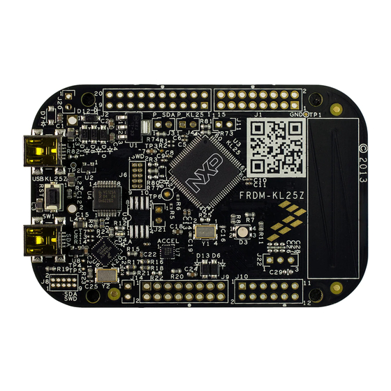
Page 4: Frdm-Kl25Z Hardware Overview
- CMSIS-DAP interface: new ARM standard for embedded debug interface - Data logging application Figure 1 shows a block diagram of the FRDM-KL25Z design. The primary components and their placement on the hardware assembly are pointed out in Figure 2. -
Page 5: Frdm-Kl25Z Hardware Description
5 FRDM-KL25Z Hardware Description 5.1 Power Supply There are multiple power supply options on the FRDM-KL25Z. It can be powered from either of the USB connectors, the V pin on the I/O header, an on-board coin cell battery, or an off-board 1.71-3.6V supply from the 3.3V pin on the I/O header. - Page 6 Coin cell battery supply voltage. Sources power to the P3V3 supply P3V3_BATT rail through a back drive protection Schottky diode. Main supply rail for the FRDM-KL25Z assembly. May be sourced from P3V3 P3V3_VREG, P3V3_BATT, or directly from the I/O headers (J9 pin 8) KL25Z MCU supply.
-
Page 7: Serial And Debug Adapter (Opensda)
10-pin (0.05”) Cortex Debug connector (J6). It is possible to isolate the KL25Z MCU from the OpenSDA circuit and use J6 to connect to an off-board MCU. To FRDMKL25ZUM FRDM-KL25Z User's Manual Page 7 of 14... -
Page 8: Virtual Serial Port
USB host and this serial interface on the KL25Z. 5.3 KL25Z Microcontroller The target microcontroller of the FRDM-KL25Z is the KL25Z128VLK4, a Kinetis L series device in an 80 LQFP package. The KL25Z MCU features include: 32-bit ARM Cortex-M0+ core... -
Page 9: Clock Source
The Kinetis KL2 microcontrollers feature an on-chip oscillator compatible with three ranges of input crystal or resonator frequencies: 32-40 kHz (low freq. mode), 3-8 MHz (high freq. mode, low range) and 8-32 MHz (high freq. mode, high range). The KL25Z128 on the FRDM-KL25Z is clocked from an 8 MHz crystal. -
Page 10: Debug
The sole debug interface on all Kinetis L Series devices is a Serial Wire Debug (SWD) port. The primary controller of this interface on the FRDM-KL25Z is the onboard OpenSDA circuit (see section 5.2). However, an unpopulated 10-pin (0.05”) Cortex Debug connector, J6, provides access to the SWD signals. -
Page 11: Input/Output Connectors
For example, the 1 pin on Port A is referred to as PTA1. The I/O connector pin names are given the same name as the KL25Z pin connected to it, where applicable. FRDMKL25ZUM FRDM-KL25Z User's Manual Page 11 of 14... -
Page 12: Arduino Compatibility
Note that all pinout data is available in spreadsheet format in FRDM-KL25Z Pinouts. See the Reference Documents section for details. 5.8 Arduino Compatibility The I/O headers on the FRDM-KL25Z are arranged to allow compatibility with peripheral boards (known as shields) that connect to Arduino™ and Arduino-compatible microcontroller boards. The outer rows of pins (the even numbered pins) on the headers share the same mechanical spacing and placement as the I/O headers on the Arduino Revision 3 (R3) standard. - Page 13 Refer to the FRDM-KL25Z Pinouts spreadsheet for a compatibility chart showing how all the functions of the KL25Z signals on the I/O connectors map to the pin functions available on the Arduino Uno R3. FRDMKL25ZUM FRDM-KL25Z User's Manual Page 13 of 14...
- Page 14 ColdFire, C_Ware, Energy Efficient Solutions logo, Kinetis, mobileGT, PowerQUICC, Processor Expert, QorIQ, Qorriva, StarCore, Symphony, and VortiQa are trademarks of Freescale Semiconductor, Inc., Reg. U.S. Pat. & Tm. Off. Airfast, BeeKit, BeeStack, ColdFire+, CoreNet, Flexis, MadniV, MXC, Platform in a Package, QorIQ Qonverge, QUICC Engine, Ready Play, SafeAssure, SMARTMOS, TurboLink, Vybrid, and Xtrinsic are trademarks of Freescale Semiconductor, Inc.
Need help?
Do you have a question about the FRDM-KL25Z and is the answer not in the manual?
Questions and answers