Table of Contents
Advertisement
Quick Links
USER MANUAL
NI Digital System Development
Board
The Digital System Development Board (DSDB) is an NI ELVIS add-on board featuring a
Zynq 7020 All Programmable SoC (AP SoC) that was designed by Digilent for National
Instruments. When paired with the NI ELVIS platform, it becomes an ideal lab installation for
classes centered on digital and analog circuits. The DSDB also has the ability to be used as a
standalone Zynq development platform, independent of NI ELVIS.
Contents
Contents .................................................................................................................................... 1
Features..................................................................................................................................... 3
Hardware Components ............................................................................................................. 5
Power Supplies ......................................................................................................................... 6
Input Power Monitoring ................................................................................................... 9
User Power Supplies......................................................................................................... 9
User Power Supplies Monitoring ..................................................................................... 10
Zynq AP SoC Architecture....................................................................................................... 11
Zynq Configuration .................................................................................................................. 15
microSD Boot Mode......................................................................................................... 16
Quad-SPI Boot Mode ....................................................................................................... 16
JTAG Boot Mode ............................................................................................................. 16
Connecting to NI ELVIS .......................................................................................................... 16
SPI Flash................................................................................................................................... 18
DDR3 Memory ......................................................................................................................... 19
USB UART Bridge (Serial Port) .............................................................................................. 20
microSD Slot ............................................................................................................................ 20
USB HID Host.......................................................................................................................... 21
HID Controller.......................................................................................................................... 21
Keyboard .................................................................................................................................. 22
Mouse ....................................................................................................................................... 24
Ethernet..................................................................................................................................... 25
OLED........................................................................................................................................ 26
VGA Port .................................................................................................................................. 29
VGA System Timing ................................................................................................................ 29
HDMI Source/Sink Port ........................................................................................................... 33
Touchscreen Display ................................................................................................................ 34
LCD Display..................................................................................................................... 34
Capacitive Touchscreen.................................................................................................... 36
Advertisement
Table of Contents

Related Manuals for National Instruments ZYNQ XC7Z020-1CLG484C


Summary of Contents for National Instruments ZYNQ XC7Z020-1CLG484C
-
Page 1: Table Of Contents
USER MANUAL NI Digital System Development Board The Digital System Development Board (DSDB) is an NI ELVIS add-on board featuring a Zynq 7020 All Programmable SoC (AP SoC) that was designed by Digilent for National Instruments. When paired with the NI ELVIS platform, it becomes an ideal lab installation for classes centered on digital and analog circuits. - Page 2 Clock Sources ........................... 39 Basic I/O ........................... 39 Seven-Segment Display ......................40 Audio ............................42 Reset Sources ..........................43 Power-on Reset ......................... 43 Program Push Button Switch.................... 44 Processor Subsystem Reset....................44 User IO Protection ........................44 Pmod Connectors ........................44 Standard Pmod ........................
-
Page 3: Features
• Four clock management tiles, each with a phase-locked loop (PLL) and mixed-mode clock manager (MMCM) • 220 DSP slices • Internal clock speeds exceeding 450 MHz NI Digital System Development Board User Manual | © National Instruments | 3... - Page 4 System Features • 512 MB DDR3 with a 32-bit bus @ 1050 MHz • 16 MB quad-SPI flash • microSD socket for additional storage • USB-JTAG programming circuitry • Current and voltage monitoring on expansion connectors • Powered from the NI ELVIS connector or 5 V barrel jack input System Connectivity •...
-
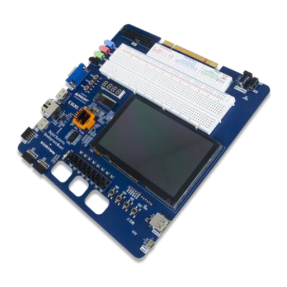
Page 5: Hardware Components
NI ELVIS II/II+ and Digital I/O from 24 Eight Slide Switches the Zynq APSoC 25 Three PMOD Connectors (Two Routed to FPGA and 13 5V Input Power Jack One Routed to Processor) NI Digital System Development Board User Manual | © National Instruments | 5... -
Page 6: Power Supplies
Power Supplies The DSDB is powered from the NI ELVIS platform or an external power supply connected to J17 (when used as a standalone platform). Connector J17 is placed in a way which doesn't allow the connection of an external supply when the board is plugged into the NI ELVIS platform. This was done to prevent the user from incorrectly attaching an external supply while the NI ELVIS is powering the DSDB. - Page 7 Table 1 provides additional information (typical currents depend strongly on FPGA configuration and the values provided are typical of medium size/speed designs). NI Digital System Development Board User Manual | © National Instruments | 7...
- Page 8 Table 1. DSDB Power Supplies Current Supply Circuits Device (max/typical) 5.125 V User Voltage, Analog Reference, IC53: 1 A/0.02 to 0.5 A Buffers for User IO ADP1613 3.3 V FPGA I/O, USB ports, Clocks, IC55#1: 2.5 A/0.1 A to Ethernet, SD slot, Flash, HDMI, User ADP5052 Voltage, LCD, touch panel, OLED 1.0 V...
-
Page 9: Input Power Monitoring
IOs that go to PMODs (JA, JB, JC), MXP (J4) and digital breadboard. This way, the communication between FPGA and the above mentioned expansion connectors is interrupted. NI Digital System Development Board User Manual | © National Instruments | 9... -
Page 10: User Power Supplies Monitoring
User Power Supplies Monitoring The users have the ability to monitor the power of the two user supplies (3.3 V and 5 V) using the dual channel analog-to-digital converter inside the Zynq (XADC). Both current and voltage information from the two user supplies are routed to auxiliary analog inputs to the XADC as differential pairs. -
Page 11: Zynq Ap Soc Architecture
PS colored light green and the PL in yellow. Note that the PCIe Gen2 controller and Multi-gigabit transceivers are not available on the device found on this board. NI Digital System Development Board User Manual | © National Instruments | 11... - Page 12 Figure 4. Zynq AP SoC Architecture The PL is nearly identical to a Xilinx 7-series Artix FPGA, except that it contains several dedicated ports and buses that tightly couple it to the PS. The PL also does not contain the same configuration hardware as a typical 7-series FPGA, and it must be configured either directly by the processor or via the JTAG port.
- Page 13 Manual, available at www.xilinx.com. Table 3 depicts the external components connected to the MIO pins of the DSDB. Table 3. MIO Pinout MIO 500 3.3 V Peripherals Peripherals Peripherals Pmod SPI Flash GPIO SCLK LED15 SLCK FB JF10 NI Digital System Development Board User Manual | © National Instruments | 13...
- Page 14 MIO 501 1.8 V Peripherals ENET 0 SDIO 0 TXCK TXD0 TXD1 TXD2 TXD3 TXCTL RXCK RXD0 RXD1 RXD2 RXD3 RXCTL 28-39 Unconnected CCLK Unconnected 48-51 Unconnected MDIO 14 | ni.com | NI Digital System Development Board User Manual...
-
Page 15: Zynq Configuration
Mode switch (SW8), which affects the state of the Zynq configuration pins after power-on. The three boot modes are described in the following sections. NI Digital System Development Board User Manual | © National Instruments | 15... -
Page 16: Microsd Boot Mode
microSD Boot Mode The DSDB supports booting from a microSD card inserted into connector J15. The following procedure will allow you to boot the Zynq from microSD: Format the microSD card with a FAT32 file system. Copy the Zynq Boot Image created with Xilinx SDK to the microSD card. Rename the Zynq Boot Image on the microSD card to BOOT.bin. - Page 17 AA16 DIO2 DIO3 AB16 DIO4 AA18 DIO5 AB15 DIO6 DIO7 AA14 DIO8 DIO9 AA19 DIO10 DIO11 AB19 DIO12 DIO13 AA17 DIO14 DIO15 AB17 PFI8 PFI9 AB20 PFI12 NI Digital System Development Board User Manual | © National Instruments | 17...
-
Page 18: Spi Flash
Table 5. NI ELVIS Zynq Connections NI ELVIS Pin Breadboard Header Breadboard Pin +15V Power +15V -15V Power -15V Power VPS+ Power VPS+ VPS- Power VPS- AIGND Analog AIGND AISENSE Analog AISNS Analog Analog AI0+ Analog AI0+ AI0- Analog AI0- AI1+ Analog AI1+... -
Page 19: Ddr3 Memory
CLK. These parameters are board-specific and were calculated from the PCB trace length reports. For more details on memory controller operation, refer to the Xilinx Zynq TRM (ug585). NI Digital System Development Board User Manual | © National Instruments | 19... -
Page 20: Usb Uart Bridge (Serial Port)
USB UART Bridge (Serial Port) The DSDB includes an FTDI FT2232HQ USB-UART bridge (attached to connector J13) that lets you use PC applications to communicate with the board using standard Windows COM port commands. Free USB-COM port drivers, available from www.ftdichip.com www.ftdichip.com under the Virtual Com Port or VCP heading, convert USB packets to UART/serial port data. -
Page 21: Usb Hid Host
(so the host device can illuminate state LEDs on the keyboard). Bus timings are shown in Figure 5. NI Digital System Development Board User Manual | © National Instruments | 21... -
Page 22: Keyboard
Figure 5. PS/2 Device-to-host Timing Diagram The clock and data signals are only driven when data transfers occur; otherwise, they are held in the idle state at logic '1'. This requires that when the PS/2 signals are used in a design, internal pull-ups must be enabled in the FPGA on the data and clock pins. - Page 23 (LSB first), followed by an odd parity bit, and terminated with a '1' stop bit. The keyboard generates 11 clock transitions (at 20 to 30 kHz) when the data is sent, and data is valid on the falling edge of the clock. NI Digital System Development Board User Manual | © National Instruments | 23...
-
Page 24: Mouse
Mouse Once entered in stream mode and data reporting enabled, the mouse outputs a clock and data signal when it is moved; otherwise, these signals idle in logic '1.' Each time the mouse is moved, three 11-bit words are sent from the mouse to the host device, as shown in Figure 11. Each of the 11-bit words contains a '0' start bit, followed by 8 bits of data (LSB first), followed by an odd parity bit, and terminated with a '1' stop bit. -
Page 25: Ethernet
The MDIO bus is available for management. The RTL8211E-VL is assigned the 5-bit address 00001 on the MDIO bus. With simple register read and write commands, status information can NI Digital System Development Board User Manual | © National Instruments | 25... -
Page 26: Oled
be read out or configuration changed. The Realtek PHY follows industry-standard register map for basic configuration. The RGMII specification calls for the receive (RXC) and transmit clock (TXC) to be delayed relative to the data signals (RXD[0:3], RXCTL and TXD[0:3], TXCTL). Xilinx PCB guidelines also require this delay to be added. - Page 27 In most cases, a 10 MHz SCLK and data sent on the falling edge should work. Figure 8. Serial Interface Timing Diagram Figure 9. OLED Serial Interface Bit Ordering NI Digital System Development Board User Manual | © National Instruments | 27...
- Page 28 Table 12. Timing Diagram Symbols and Parameters Symbol Parameter Unit Clock Cycle Time cycle Address Setup Time Address Hold Time Chip Select Setup Time Chip Select Hold Time Write Data Setup Time Write Data Hold Time Clock Low Time CLKL Clock High Time CLKH Rise Time...
-
Page 29: Vga Port
(one for red, one for blue, and one for green) to energize the phosphor that coats the inner side of the display end of a cathode ray tube (see Figure 10). NI Digital System Development Board User Manual | © National Instruments | 29... - Page 30 Figure 10. Color CRT Display Electron beams emanate from electron guns which are finely-pointed heated cathodes placed in close proximity to a positively charged annular plate called a grid. The electrostatic force imposed by the grid pulls rays of energized electrons from the cathodes, and those rays are fed by the current that flows into the cathodes.
- Page 31 The VS signal defines the refresh frequency of the display, or the frequency at which all information on the display is redrawn. The minimum refresh NI Digital System Development Board User Manual | © National Instruments | 31...
- Page 32 frequency is a function of the display’s phosphor and electron beam intensity, with practical refresh frequencies falling in the 50 Hz to 120 Hz range. The number of lines to be displayed at a given refresh frequency defines the horizontal retrace frequency. For a 640-pixel by 480-row display using a 25 MHz pixel clock and 60 ±1 Hz refresh, the signal timings shown in Figure 12 can be derived.
-
Page 33: Hdmi Source/Sink Port
HDMI specifications only require terminations on the Sink side, but optional Source-side terminations reduce reflections, resulting in improved signal quality. Do not connect powered HDMI/DVI devices to an unpowered NI Digital System Development Board User Manual | © National Instruments | 33... -
Page 34: Touchscreen Display
DSDB, as it might result in back-powering the board through the termination resistors. Resolutions up to 720p (1280 × 720) have been tested. HDMI and DVI are high-speed source-synchronous serial protocols. Implementations on FPGA are required to use certain built-in primitives to properly synthesize the correct clock frequency, serialize the transmission, and keep a lock on the signal. - Page 35 Table 16. Horizontal Timing Horizontal Input Timing Parameter Symbol Value Unit Min. Typ. Max. Active Area — — CLKIN CLKIN frequency fclk — 33.3 Horizontal line period 1056 1200 CLKIN NI Digital System Development Board User Manual | © National Instruments | 35...
-
Page 36: Capacitive Touchscreen
Table 16. Horizontal Timing (Continued) Horizontal Input Timing Horizontal pulse Min. thpw — — CLKIN width Typ. — — — CLKIN Max. — — CLKIN Horizontal back porch thbp CLKIN Horizontal front porch thfp CLKIN Figure 15. Vertical Timing Table 17. Vertical Timing Vertical Input Timing Parameter Symbol... - Page 37 100b FACTORY MODE0 (Reserved) 110b FACTORY MODE1 (Reserved) This register describes MSB of the X coordinate of the nth touch point and the corresponding event flag.(Read only) NI Digital System Development Board User Manual | © National Instruments | 37...
- Page 38 Table 20. X MSB Register Address Address Register Name Description 03h ~ 1Bh Event Flag 00b: Press Down 01b: Lift Up 10b: Contact 11b: No event Reserved Touch X Position MSB of Touch X Position in pixels [11:8] This register describes LSB of the X coordinate of the nth touch point.(Read only) Table 21.
-
Page 39: Clock Sources
The LED attached directly to the PS are accessed using the Zynq GPIO controller. This core is described in full in Chapter 14 of the Zynq Technical Reference Manual. NI Digital System Development Board User Manual | © National Instruments | 39... -
Page 40: Seven-Segment Display
Seven-Segment Display The DSDB contains a four-digit common anode seven-segment LED display. Each of the four digits is composed of seven segments arranged in a “figure 8” pattern, with an LED embedded in each segment. Segment LEDs can be individually illuminated, so any one of 128 patterns can be displayed on a digit by illuminating certain LED segments and leaving the others dark, as shown in Figure 16. - Page 41 An example timing diagram for a four-digit controller is shown in Figure 18. Figure 18. Four Digit Scanning Display Controller Timing Diagram NI Digital System Development Board User Manual | © National Instruments | 41...
-
Page 42: Audio
Audio An Analog Devices SSM2603 Audio Codec provides integrated digital audio processing to the Zynq programmable logic. It allows for stereo record and playback at sample rates from 8 kHz to 96 kHz. On the analog side, the codec connects to four 3.5 mm standard audio jacks. There are two inputs: a mono microphone and a stereo line in. -
Page 43: Reset Sources
Zynq power-on reset by pressing the red button labeled “PS-PORB”. This (or a power cycle) is necessary whenever the boot mode is changed using SW8. NI Digital System Development Board User Manual | © National Instruments | 43... -
Page 44: Program Push Button Switch
Program Push Button Switch The red “PROGB” push button, BTN5, toggles the Zynq’s PROG_B signal. This resets the PL and causes DONE to be de-asserted. The PL will remain unconfigured until it is reprogrammed by the processor or via JTAG. Processor Subsystem Reset The External system reset push button, labeled “PS-SRSTB”, resets the Zynq device without disturbing the debug environment. -
Page 45: Standard Pmod
PS peripheral controller cores. The GPIO, UART, I2C, and SPI cores can all be used to drive devices connected to this Pmod. Note that the pin layout of the UART and I2C NI Digital System Development Board User Manual | © National Instruments | 45... -
Page 46: Mxp Connector
cores will not align perfectly with the typical Pmod pinouts for these interfaces. This means that UART or I2C devices connected to this Pmod may require some of the pins to be swapped around externally using individual wires between the DSDB and the Pmod. MXP Connector The myRIO Extension Port (MXP) Connector is a standard connector interface designed by NI to provide an interoperable ecosystem of educational add-ons. -
Page 47: Breadboards
Figure 22. Signal Breadboards with Pinout Each of the three signal breadboards has different functions described in the following sections. NI Digital System Development Board User Manual | © National Instruments | 47... -
Page 48: Ni Elvis Analog Breadboard
NI ELVIS Analog Breadboard This breadboard gives access to the analog capabilities of the NI ELVIS development system. Analog signals are routed directly from the NI ELVIS edge connector to the breadboard. Pin markings on the breadboard match the NI ELVIS signal naming convention. For detailed information visit the NI ELVIS II Series User Manual and NI ELVIS II Series Specifications, available at ni.com/manuals... - Page 49 In the Project Explorer window FPGA Target (DSDB, Digital System Development Board) tree view, select SW0 and LED0 and drag them onto the block diagram as shown in the image below. NI Digital System Development Board User Manual | © National Instruments | 49...
- Page 50 In the LabVIEW block diagram, wire SW0 output to the LED0 input. In the Project Explorer window FPGA Target (DSDB, Digital Systems Development Board) tree view, select BTN0 and LED2 and drag them onto the block diagram. In the LabVIEW block diagram, wire BTN0 output to the LED2 input. Add a While Loop around the resources.
- Page 51 When the compilation finishes, click Stop Server to close the LabVIEW FPGA Compile Server. Click Close in the Successful Compile Report window as shown in the image below. NI Digital System Development Board User Manual | © National Instruments | 51...
- Page 52 The application is running on the FPGA board at this time. Move switch SW0 up and down; LED0 should correspondingly light and turn off. Press button BTN0; LED2 should correspondingly light and turn off. More DSDB examples can be found in the LabVIEW Example Finder. In LabVIEW Click Help»Find Examples.
-
Page 53: Programming In Multisim
Install LabVIEW 2015 FPGA Module Xilinx Tools Vivado 2014.4 or later. Install the Digilent drivers. Navigate to and select the latest version of Vivado installed. C:\NIFPGA\Programs Continue to navigate through to …\data\xicom\cable_drivers\nt64\digilent install_digilent.exe NI Digital System Development Board User Manual | © National Instruments | 53... - Page 54 Procedure Creating a Project In Multisim, select File»New. Click PLD Design, then click Create. 54 | ni.com | NI Digital System Development Board User Manual...
- Page 55 Click the Use standard configuration down arrow and select your board. Click Next. NI Digital System Development Board User Manual | © National Instruments | 55...
- Page 56 Enter in the PLD design name field and Introduction to Digital Electronics click Next. The New PLD Design dialog allows you to select which peripherals you will use in your design. Ensure the LED LED0 and the push button BTN0 are selected. Click Finish. 56 | ni.com | NI Digital System Development Board User Manual...
- Page 57 The selected connectors are placed on the workspace. NI Digital System Development Board User Manual | © National Instruments | 57...
- Page 58 Create a PLD Schematic in Multisim Select Place»Component. Select an AND2 gate located in the PLD Logic group, Logic_gates family and click OK. Place another connector for the AND gate input by clicking the Input connector icon on the toolbar. 58 | ni.com | NI Digital System Development Board User Manual...
- Page 59 Generate and save the VHDL—This option exports the VHDL netlist, allowing students to view the VHDL code. You can import the VHDL code in the Xilinx environment and program the FPGA NI Digital System Development Board User Manual | © National Instruments | 59...
- Page 60 In this tutorial you will program the FPGA board directly from the Multisim environment. Select Transfer»Export to PLD. Click Program the connected PLD and then click Next. In the Select a tool to use area, select the Xilinx tool for your board. 60 | ni.com | NI Digital System Development Board User Manual...
- Page 61 Multisim will automatically open the Xilinx tool in the background and perform all the requires steps to program the FPGA, no user interacting is required. NI Digital System Development Board User Manual | © National Instruments | 61...
-
Page 62: Installation And Setup
Once the FPGA is programmed, Multisim will display a message on the Spreadsheet View. You can now test the design built in Multisim on the physical hardware. Installation and Setup This section describes what you need to get started with the DSDB and how to install your software and set up your board. -
Page 63: Installation And Setup Instructions
For patents covering NI products/technology, refer to the appropriate location: Help»Patents in your software, the patents.txt file on your media, or the National Instruments Patents Notice at ni.com/patents. You can find information about end-user license agreements (EULAs) and third-party legal notices in the readme file for your NI product.
Need help?
Do you have a question about the ZYNQ XC7Z020-1CLG484C and is the answer not in the manual?
Questions and answers