
Related Manuals for NI PXIe-6674T


Summary of Contents for NI PXIe-6674T
- Page 1 PXI Express NI PXIe-6674T User Manual Timing and Synchronization Module for PXI Express NI PXIe-6674T User Manual May 2015 373089C-01...
- Page 2 National Instruments Corporate Headquarters 11500 North Mopac Expressway Austin, Texas 78759-3504 USA Tel: 512 683 0100 For further support information, refer to the NI Services appendix. To comment on National Instruments documentation, refer to the National Instruments website at ni.com/info...
- Page 3 You must obtain an RMA number from NI before returning any product to NI. NI reserves the right to charge a fee for examining and testing Hardware not covered by the Limited Warranty.
- Page 4 LEAD TO DEATH, PERSONAL INJURY, SEVERE PROPERTY DAMAGE OR ENVIRONMENTAL HARM (COLLECTIVELY, “HIGH-RISK USES”). FURTHER, PRUDENT STEPS MUST BE TAKEN TO PROTECT AGAINST FAILURES, INCLUDING PROVIDING BACK-UP AND SHUT-DOWN MECHANISMS. NI EXPRESSLY DISCLAIMS ANY EXPRESS OR IMPLIED WARRANTY OF FITNESS OF THE PRODUCTS OR SERVICES FOR HIGH-RISK...
- Page 5 The Declaration of Conformity (DoC) contains important EMC compliance information and instructions for the user or installer. To obtain the DoC for this product, visit , search by ni.com/certification model number or product line, and click the appropriate link in the Certification column.
-
Page 6: Table Of Contents
Installing the Software...................... 2-1 Installing the Hardware ....................2-1 Configuring the Module ....................2-2 Chapter 3 Hardware Overview NI PXIe-6674T Front Panel ..................... 3-3 Access LED ......................3-4 Active LED....................... 3-5 Connectors ........................ 3-5 Hardware Features ......................3-6 Generating and Routing Clocks..................3-8 Clock Generation...................... - Page 7 Contents Chapter 4 Calibration Factory Calibration ......................4-1 OCXO Frequency ..................... 4-1 PXI_CLK10 Phase....................4-1 Additional Information ..................... 4-1 Appendix A Specifications Appendix B NI Services Glossary Index viii | ni.com...
-
Page 8: About This Manual
Thank you for purchasing the National Instruments NI PXIe-6674T Timing and Synchronization Module. The NI PXIe-6674T enables you to pass PXI timing and trigger signals between PXI Express chassis. The NI PXIe-6674T can generate and route clock signals between devices in multiple chassis, providing a method to synchronize multiple devices in a multichassis PXI Express system. -
Page 9: Introduction
PXI Express embedded controller or a desktop computer connected to the PXI Express chassis using MXI-Express hardware The NI-Sync User Manual offers more detailed information on the software used to program the NI PXIe-6674T. You can find this manual on the NI-Sync CD or download it from ni.com/ manuals... -
Page 10: Unpacking
Remove the module from the package and inspect the module for loose components or any sign of damage. Notify NI if the module appears damaged in any way. Do not install a damaged module into the computer. - Page 11 NI PXIe-6674T User Manual Do not operate the product in an explosive atmosphere or where there may be flammable gases or fumes. If you must operate the product in such an environment, it must be in a suitably rated enclosure.
- Page 12 • Measurement Category IV is for measurements performed at the primary electrical supply installation typically outside buildings. Examples include electricity meters and measurements on primary overcurrent protection devices and on ripple control units. 1-4 | ni.com...
-
Page 13: Installing And Configuring
Installing and Configuring This chapter describes how to install the NI PXIe-6674T hardware and software and how to configure the device. Installing the Software Refer to the file that accompanies the NI-Sync CD for software installation readme.htm directions. Be sure to install the driver software before installing the NI PXIe-6674T Note hardware. -
Page 14: Configuring The Module
Plug in and power on the chassis. The NI PXIe-6674T is now installed. Configuring the Module The NI PXIe-6674T is completely software configurable. The system software automatically allocates all module resources. The two LEDs on the front panel provide information about module status. The front panel... -
Page 15: Hardware Overview
Hardware Overview This chapter presents an overview of the hardware functions of the NI PXIe-6674T. Figure 3-1 provides a functional overview of the NI PXIe-6674T hardware. © National Instruments | 3-1... - Page 16 Chapter 3 Hardware Overview Figure 3-1. Functional Overview of the NI PXIe-6674T PXI_CLK10_IN AC Coupled CLKIN Clock Detector OCXO OCXO OCXO Clock Calibration PXI_CLK10 CLKOUT PXIe_CLK100 Clock Generation CLKIN PXIe_DSTARA Clock Generation <0..16> PXIe_DSTARA Routing PXIe_DSTARC LVDS Driver/ <0..16> Receiver...
-
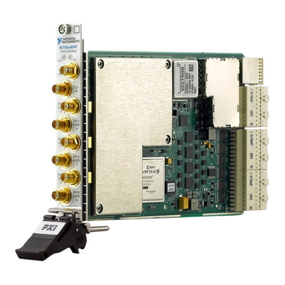
Page 17: Ni Pxie-6674T Front Panel
NI PXIe-6674T User Manual NI PXIe-6674T Front Panel Figure 3-2 shows the connectors and LEDs on the front panel of the NI PXIe-6674T. Figure 3-2. NI PXIe-6674T Front Panel NI PXIe-6674T Timing Module PFI 0/ LVDS PFI 1/ LVDS PFI 2/... -
Page 18: Access Led
Chapter 3 Hardware Overview Access LED The Access LED indicates the communication status of the NI PXIe-6674T. Refer to Figure 3-2 for the location of the Access LED. Table 3-1 summarizes what the Access LED colors represent. Table 3-1. Access LED Color Indication... -
Page 19: Active Led
Connections that exceed any of the maximum ratings of input or output Caution signals on the NI PXIe-6674T can damage the module and the computer. NI is not liable for any damage resulting from such signal connections. © National Instruments | 3-5... -
Page 20: Hardware Features
Chapter 3 Hardware Overview Hardware Features The NI PXIe-6674T performs two broad functions: • Generating clock and trigger signals • Routing internally or externally generated signals from one location to another Table 3-3 outlines the function and direction of the signals discussed in detail in the remainder of this chapter. - Page 21 The PXI trigger bus consists of eight digital lines (to/from shared among all slots in the PXI Express chassis. chassis) The NI PXIe-6674T can route a wide variety of signals to and from these lines. Note: PXI_TRIG<0..5> are also known as RTSI<0..5> in some hardware devices and APIs.
-
Page 22: Generating And Routing Clocks
PXI chassis. Generating and Routing Clocks The NI PXIe-6674T can generate two types of clock signals. The first clock is generated using the onboard clock generation circuitry, and the second is generated with a precise 10 MHz oscillator. -
Page 23: Pxi_Clk10 And Pxie_Clk100
The individual components which make up the clock generation circuitry are controlled by NI-Sync software, which allows the user to simply specify the frequency they wish the clock generation circuitry to produce. NI-Sync will then configure the clock generation circuitry to give the closest possible frequency match to the requested frequency and do so with the configuration that gives the lowest possible phase noise. -
Page 24: Using Pxi_Clk10_In
The OXCO used by the NI PXIe-6674T features electronic frequency control. This allows the OCXO to be fine-tuned by varying the control voltage to the OCXO. The NI PXIe-6674T uses a 16-bit digital analog converter to give precise control of the tuning voltage. While the tuning voltage can be varied by the user, it is normally controlled automatically by software which sets it to the calibration tuning voltage. -
Page 25: Pxie_Dstara, Pxie_Dstarb, And Pxie_Dstarc
By increasing or decreasing the frequency of the OCXO as needed, the 10 MHz PLL of the NI PXIe-6674T is able to match the OCXO frequency to the reference clock supplied by the user from CLKIN. - Page 26 The NI PXIe-6674T receives each PXIe_DSTARC signal and sends a copy to the PXIe_DSTARA network for clock sharing and to the FPGA for trigger routing.
- Page 27 NI PXIe-6674T User Manual The PXIe_DSTARA network allows the user to select which source to route to the PXIe_DSTARA lines. It does this by creating two intermediate sources, Source A and Source B. Source A and Source B are created by multiplexers with the source options shown in Table 3-5.
- Page 28 Table 3-8. Inputs and Outputs of the Cross Point Switch Inputs Outputs PXIe_DSTARA Network Bank 0 PFI_LVDS 0 PXIe_DSTARA Network Bank 1 PFI_LVDS 1 PXIe_DSTARA Network Bank 2 PFI_LVDS 2 Clock Generation High Speed CLKOUT 3-14 | ni.com...
- Page 29 The CLKOUT SMA connector on the front panel provides a means to export a clock signal from the NI PXIe-6674T to an external device or another system timing module. The CLKOUT driver uses two separate circuits for driving CLKOUT, one for low speed frequencies (50 MHz and below) and one for high speed (above 50 MHz).
-
Page 30: Routing Signals
Hardware Overview Routing Signals The NI PXIe-6674T has versatile trigger routing capabilities. It can route signals to and from the front panel, the PXI star triggers, the PXI triggers, and PXIe_DSTARB/PXIe_DSTARC. Figures 3-4 and 3-5 summarize the routing features of the NI PXIe-6674T. The remainder of this chapter details the capabilities and constraints of the routing architecture. -
Page 31: Determining Sources And Destinations
Table 3-9 summarizes the sources and destinations of the NI PXIe-6674T. The destinations are listed in the horizontal heading row, and the sources are listed in the column at the far left. A ... - Page 32 Table 3-9. Sources and Destinations for NI PXIe-6674T Signal Routing Operations Destinations Front Panel Backplane board PXI Star PXIe OCXO LVDS Trigger TRIG SYNC D STARA D STARB <0..5> <0..2> 10 IN <0..16> <0..7> CTRL <0..16> <0..16> ...
- Page 33 Software Trigger † Routing PXI_CLK10, PXIe_CLK100, OCXO or ClkGen is accomplished by setting the synchronization clock (NI-Sync Property Node) to the desired clock source and then routing the synchronization clock as the source. Route through the FPGA. Route to PFI LVDS can be made through the FPGA when used as a trigger, or through the PXIe-DTARA network when used as a clock.
-
Page 34: Using Front Panel Pfis As Single Ended Inputs
Terminating the signals with a 50 Ω resistance is recommended when the Note source is another NI PXIe-6674T or any other source with a 50 Ω output. The voltage thresholds for the front-panel PFI inputs are programmable. The input signal is generated by comparing the input voltage on the PFI connectors to the voltage output of software-programmable DACs. -
Page 35: Using Front Panel Pfis For Lvds Triggers
NI PXIe-6674T User Manual • Any of the previously listed signals divided by the first frequency divider (2 , up to 512) • Any of the previously listed signals divided by the second frequency divider (2 , up to 512) -
Page 36: Using The Pxi Triggers
, up to 512) • Any of the previously listed signals divided by the second frequency divider (2 , up to 512) Refer to the Choosing the Type of Routing section for more information about the synchronization clock. 3-22 | ni.com... -
Page 37: Using The Pxi Star Triggers
1 ns. A typical upper limit for the skew in most NI PXI Express chassis is 500 ps. The low skew of the PXI star trigger bus is useful for applications that require triggers to arrive at several modules nearly simultaneously. -
Page 38: Choosing The Type Of Routing
Choosing the Type of Routing The NI PXIe-6674T routes signals in one of two ways: asynchronously or synchronously. The following sections describe the two routing types and the considerations for choosing each type. Asynchronous Routing Asynchronous routing is the most straightforward method of routing signals. -
Page 39: Synchronous Routing
Propagation delay of the signal through the NI PXIe-6674T • Time for the receiver to recognize the signal Both the source and the destination of an asynchronous routing operation on the NI PXIe-6674T can be any of the following lines: •... - Page 40 Synchronous routing can send triggers to several places in the same clock cycle. If a signal arrives at two chassis within the same clock cycle, each NI PXIe-6674T realigns the signal with the synchronization clock and distributes it to the modules in each chassis at the same time.
- Page 41 NI PXIe-6674T includes two clock-divider circuits that can divide the synchronization clock signals by any power of 2 up to 512. Refer to Figures 3-4 and 3-5 for an illustration of how the NI PXIe-6674T performs synchronous routing operations. © National Instruments | 3-27...
-
Page 42: Factory Calibration
(EEPROM). The driver software uses these stored values. Factory Calibration The factory calibration of the NI PXIe-6674T involves calculating and storing four calibration constants. These values control the accuracy of two features of the device, which are discussed in the following sections. -
Page 43: Appendix A Specifications
Specifications This appendix lists the system specifications for NI PXIe-6674T modules. These specifications are typical at 25 °C, unless otherwise stated. Specifications are subject to change without notice. Note Some specifications are specific to earlier revisions of the NI PXIe-6674T Note module. - Page 44 Operation above the Absolute Maximum Input Powered On may cause damage to the device. Absolute Maximum Input Powered Off is the maximum input signal amplitude that the device can tolerate before damage might occur while in an unpowered state. Input can be either square wave or sinusoidal. Note A-2 | ni.com...
- Page 45 NI PXIe-6674T User Manual Figure A-2. Maximum and Minimum Input Swing with Attenuation On Input Duty Cycle (%) Minimum Input Swing (Vpp) Maximum Input Swing (Vpp) Figure A-3. Maximum and Minimum Input Swing with Attenuation Off Input Duty Cycle Minimum frequency ......... 1 MHz Maximum frequency To Clk10PLL ..........
- Page 46 Recommended calibration interval ....1 year Maximum Phase Noise of the OCXO Offset Phase Noise 1 Hz -80 dBc/Hz 10 Hz -120 dBc/Hz 100 Hz -140 dBc/Hz 1 kHz -145 dBc/Hz 10 kHz -150 dBc/Hz After 72 hours of continuous operation. A-4 | ni.com...
- Page 47 NI PXIe-6674T User Manual Figure A-4 shows the phase noise on a representative module. OCXO is routed to the ClkOut SMA, measured in a NI PXIe-1082 chassis with low fan speed . The integrated jitter from 10 Hz to 1 MHz is 507 fs rms.
- Page 48 Figure A-5 shows the phase noise on a representative module of PXI_CLK10 when OCXO is routed to PXI_CLK10_IN , measured in a NI PXIe-1082 chassis with low fan speed: Figure A-5. Phase Noise on a Representative Module of PXI_CLK10 when OCXO is routed to PXI_CLK10_IN –50...
- Page 49 NI PXIe-6674T User Manual Figure A-6 shows the phase noise on a representative module of PXI_CLK10 when CLKIN is routed to PXI_CLK10_IN with and without the 10 MHz PLL, measured in a NI PXIe-1082 chassis with low fan speed Figure A-6. Phase Noise on a Representative Module of PXI_CLK10 with CLKIN Routing to PXI_CLK10_IN –50...
- Page 50 PXIe-DStarA Network Operation of low speed ClkOut above 50 MHz is possible however NI does not guarantee performance. Use ClkOutLS as the destination terminal to force NI-Sync to use the low speed driver above 50 MHz. † Operation above 1 GHz is possible but NI does not guarantee performance.
- Page 51 NI PXIe-6674T User Manual Figure A-7 shows the typical Low Speed ClkOut Amplitude performance, with a sample size of 19 modules. Figure A-7. Typical Low Speed ClkOut Amplitude Performance 2.75 2.65 2.55 2.45 Frequency (MHz) Figure A-8 shows the typical High Speed ClkOut Amplitude performance, with a sample size of 19 modules.
- Page 52 = .2794 Hz. When routed to ClkOut High Speed the minimum frequency is 4.6875 MHz. Use ClkOutHS as the destination terminal to force NI-Sync to use the low speed driver below 50 MHz. Note that AC coupling on ClkOut limits the minimum frequency which can be used.
- Page 53 All Phase Noise Measurements were made on a Representative Module of Note various Clock Generation frequencies routed to ClkOut. All Measurement made in an NI PXIe-1062 chassis with low fan speed and OCXO connected to PXI_Clk10_IN. The phase noise performance of the clock generation circuitry varies depending on what elements are used to generate the requested frequency.
- Page 54 Figure A-10. Phase Noise of Frequencies From the Multiplying PLL –70 A. 300 MHz –75 B. 500 MHz –80 C. 1 GHz –85 –90 –95 –100 –105 –110 –115 –120 –125 –130 –135 –140 –145 –150 100k Frequency Offset (Hz) A-12 | ni.com...
- Page 55 –110 –115 –120 –125 –130 –135 –140 –145 –150 –155 –160 –165 –170 100k Frequency Offset (Hz) Use ClkOutHS as the destination terminal to force NI-Sync to use the high speed driver below 50 MHz. © National Instruments | A-13...
- Page 56 275 ps ClkIn to PXIe-DStarA Delay Typical at 25 °C ........4.21 ns Maximum over temperature......4.36 ns PXIe-DStarA to PXIe-DStarA Skew Typical............<100 ps Maximum over temperature......250 ps Maximum Frequency may exceed 1 GHz however performance is not guaranteed. A-14 | ni.com...
- Page 57 NI PXIe-6674T User Manual Triggers PFI Single Ended Input Characteristics Termination Setting High Impedance 50 Ω Input Impedance 10 kΩ, ± 20% 50 Ω, ± 5% Input Coupling Hysteresis 50 mV typical 58 mV typical (Revision C and D) ‡‡...
- Page 58 100 mV would cause the applied voltage to fall below 0 V and therefore would not be acceptable. ‡ Operation beyond 1 GHz is possible but performance is not guaranteed. Operation beyond 200 MHz is possible but performance is not guaranteed. This limitation comes from the FPGA, not the LVDS receiver. A-16 | ni.com...
- Page 59 NI PXIe-6674T User Manual Output Characteristics Differential Output Voltage into 100 ohm differential load (at DC) 600 mV typical Output Common Mode Voltage 1.125 V to 1.375 V Maximum Output Frequency—Sourced from Cross Point Switch 1 GHz † Maximum Output Frequency—Sourced from FPGA...
- Page 60 I/O Voltage Level..........3.3 V CMOS, 5 V input tolerant PXIe-DStarB The PXIe-DStarB signals are LVDS signals that allow the NI PXIe-6674T to route high speed trigger signals to any other PXIe slot in a chassis. Each PXI Express slot in a chassis has its own PXIe-DStarB connection with the System Timing Slot.
- Page 61 NI PXIe-6674T User Manual Trigger Timing Asynchronous Trigger Delays and Skew Table A-1. Asynchronous Trigger Delays and Skew Values † Trigger Source Trigger Destination Typical Delay Typical Skew Single Ended PFI Single Ended PFI 23.4 ns <.5 ns Single Ended PFI LVDS PFI 22.4 ns...
- Page 62 13.0 ns <.5 ns Typical Delay is measured from the input to the NI PXIe-6674T at the connector to the output at the connector. For example, Single Ended PFI to PXI-Star is the delay from the Single Ended PFI SMA connector to the PXI-Star at the backplane connector.
- Page 63 NI PXIe-6674T User Manual Synchronized Trigger Setup and Hold Timing with Respect to PXI-Clk10 Table A-3. Synchronized Trigger Setup and Hold Timing With Respect to PXI_Clk10 † Trigger Source Trigger Destination Setup Time Hold Time Single Ended PFI Single Ended PFI 11.2 ns Typical,...
- Page 64 Hold Time is the amount of time after a rising edge of PXI-Clk10 (at the backplane connector) that a logic level must be valid on the trigger source (at the connector) in order for the trigger destination to update. Refer to the Synchronous Routing section of Chapter 3, Hardware Overview, for more information. A-22 | ni.com...
- Page 65 FPGA Functionality Trigger Routing Table A-4 shows the routes that can be made. Table A-4. Sources and Destinations for NI PXIe-6674T Signal Routing Operations Destinations Front Panel Backplane board PXI Star PXIe OCXO LVDS Trigger TRIG SYNC D STARA D STARB <0..5>...
- Page 66 Software Trigger † Routing PXI_CLK10, PXIe_CLK100, OCXO or ClkGen is accomplished by setting the synchronization clock (NI-Sync Property Node) to the desired clock source and then routing the synchronization clock as the source. Route through the FPGA. Route to PFI LVDS can be made through the FPGA when used as a trigger, or through the PXIe-DTARA network when used as a clock.
- Page 67 Operation beyond 200 MHz is possible but performance is not guaranteed. Accuracy of frequency measurement is relative to the frequency accuracy of the reference counter source. The frequency measure vi in NI-Sync does not account for error from the reference source. © National Instruments | A-25...
-
Page 68: Operating Environment
(Tested in accordance with IEC 60068-2-64. Nonoperating test profile exceeds the requirements of MIL-PRF-28800F, Class 3.) Clean the NI PXIe-6674T module with a soft nonmetallic brush. Make Caution sure that the device is completely dry and free from contaminants before returning it to service. - Page 69 For additional environmental information, refer to the Minimize Our Environmental Impact web page at . This page contains the environmental regulations and ni.com/environment directives with which NI complies, as well as other environmental information not included in this document. © National Instruments | A-27...
- Page 70 WEEE recycling center. For more information about WEEE recycling centers, National Instruments WEEE initiatives, and compliance with WEEE Directive 2002/96/EC on Waste and Electronic Equipment, visit ni.com/environment/ weee National Instruments (RoHS) National Instruments RoHS ni.com/ (For information about China RoHS compliance, environment/rohs_china go to ni.com/environment/rohs_china A-28 | ni.com...
- Page 71 – Warranty and Repair—All NI hardware features a one-year standard warranty that is extendable up to five years. NI offers repair services performed in a timely manner by highly trained factory technicians using only original parts at a National Instruments service center.
- Page 72 KnowledgeBase, product manuals, step-by-step troubleshooting wizards, thousands of example programs, tutorials, application notes, instrument drivers, and so on. Registered users also receive access to the NI Discussion Forums . NI Applications Engineers make sure every question submitted ni.com/forums...
- Page 73 Glossary Symbol Prefix Value femto pico nano µ micro milli kilo mega giga Symbols percent ± plus or minus positive, or plus negative, or minus ° degree Ω accumulator a part where numbers are totaled or stored application development environment asynchronous a property of an event that occurs at an arbitrary time, without synchronization to a reference clock...
- Page 74 A/D and/or DIO devices plugged into a computer, and possibly generating control signals with D/A and/or DIO devices in the same computer direct current direct digital synthesis—a method of creating a clock with a programmable frequency G-2 | ni.com...
- Page 75 NI PXIe-6674T User Manual EEPROM electrically erasable programmable read-only memory—ROM that can be erased with an electrical signal and reprogrammed electrostatic discharge frequency the rate of events or oscillations per second, measured with a frequency counter or spectrum analyzer. Frequency is the reciprocal of the period of a signal.
- Page 76 PCI eXtensions for Instrumentation—An open implementation of CompactPCI Express that adds electrical features that meet the high-performance requirements of instrumentation applications by providing triggering, local buses, and system clock capabilities. PXI Express also offers two-way interoperability with CompactPCI Express products. G-4 | ni.com...
- Page 77 PXI Express peripheral slot (up to 17 peripheral slots) PXIe_DStarC RTSI bus Real-Time System Integration bus—the NI timing bus that connects DAQ devices directly, by means of connectors on top of the devices, for precise synchronization of functions. In a PXI or PXI Express system these are referred to as the PXI-Triggers.
- Page 78 CtoQ hold time hold propagation delay time TRIG trigger signal trigger a digital signal that starts or times a hardware event (for example, starting a data acquisition operation) setup time setup volts virtual instrument G-6 | ni.com...
- Page 79 3-25 Access LED, 3-4 timing diagram, 3-24 Active LED, 3-5 overview, 2-2 block diagram NI PXIe-6674T functional overview, 3-2 destinations, possible destinations (table), routing architecture, 3-16 3-18, A-23 signal selection circuitry, 3-17 documentation, related documentation, ix cable configuration, 3-20...
- Page 80 (caution), 3-5 using front panel PFIs as outputs, 3-20 PFI_LVDS <0..2> signal description (table), 3-7 phase-locked loop. See PLL NI PXIe-6674T physical specifications, A-25 configuration, 2-2 PLL, routing from the CLKIN connector, 3-5 connectors, 3-5 power requirement specifications, A-25 functional overview, 3-6 programmable function interface.
- Page 81 NI PXIe-6674T User Manual using front panel PFIs as LVDS routing signals triggers, 3-21 front panel triggers using front panel PFIs as outputs, 3-20 using as LVDS triggers, 3-21 using the PXI triggers, 3-22 using as single ended inputs, 3-20...
- Page 82 3-25 unpacking the device, 1-2 possible sources and destinations, 3-26 synchronization clock sources, 3-27 timing diagram, 3-26 voltage thresholds, programming, 3-20 terminating signals with resistors (note), 3-20 threshold, voltage, 3-20 trigger bus. See PXI_TRIG I-4 | ni.com...
Need help?
Do you have a question about the PXIe-6674T and is the answer not in the manual?
Questions and answers