Yamaha TF5 Service Manual
Digital mixing console
Hide thumbs
Also See for TF5:
- Reference manual (91 pages) ,
- User manual (75 pages) ,
- Service manual (45 pages)
Advertisement
CONTENTS(目次)
SPECIFICATIONS(総合仕様) ................................. 4
PANEL LAYOUT(パネルレイアウト) ...................... 5
DIMENSIONS(寸法図) .......................................... 10
(TF5 ユニットレイアウト) ..................................... 12
(TF3 ユニットレイアウト) ..................................... 15
(TF1 ユニットレイアウト) ..................................... 18
TF5 DISASSEMBLY PROCEDURE(TF5 分解手順) .... 21
TF3 DISASSEMBLY PROCEDURE(TF3 分解手順) .... 44
TF1 DISASSEMBLY PROCEDURE(TF1 分解手順) .... 67
LSI PIN DESCRIPTION(LSI 端子機能表) ............. 90
CIRCUIT BOARDS(シート基板図) ..................... 106
TEST PROGRAM(テストプログラム) ......... 128/161
PA
012144
201404-オープンプライス
DIGITAL MIXING CONSOLE
/
SERVICE MANUAL
SERVICE MANUAL
TF3
SETTINGS FOR SHIPMENT(出荷設定) .... .. 160/193
(フェーダキャリブレーション) ..................... 194/196
INITIALIZATION(初期化) ..................................... 198
FIRMWARE (HOST CPU AND OTHER SUB CPU)
UPDATER BY USB MEMORY
及び、他のサブマイコン)書き込み方法) ............. 199/201
SEQUENCE(シーケンス) ............................. 203/206
PARTS LIST
BLOCK DIAGRAM(ブロックダイアグラム)
OVERALL CONNECTOR CIRCUIT DIAGRAM
(総コネクタ接続回路図)
CIRCUIT DIAGRAM(回路図)
Copyright (c) Yamaha Corporation. All rights reserved. PDF
/
TF5
TF1
HAMAMATSU, JAPAN
'15.05
Advertisement
Chapters

Related Manuals for Yamaha TF5


Summary of Contents for Yamaha TF5
-
Page 1: Table Of Contents
TF1 DISASSEMBLY PROCEDURE(TF1 分解手順) ..67 OVERALL CONNECTOR CIRCUIT DIAGRAM LSI PIN DESCRIPTION(LSI 端子機能表) ..... 90 (総コネクタ接続回路図) CIRCUIT BOARDS(シート基板図) ..... 106 CIRCUIT DIAGRAM(回路図) TEST PROGRAM(テストプログラム) ..128/161 012144 HAMAMATSU, JAPAN 201404-オープンプライス Copyright (c) Yamaha Corporation. All rights reserved. PDF ’15.05... -
Page 2: Important Notice
IMPORTANT NOTICE This manual has been provided for the use of authorized Yamaha Retailers and their service personnel. It has been assumed that basic service procedures inherent to the industry, and more specifically Yamaha Products, are already known and understood by the users, and have therefore not been restated. -
Page 3: Backup Battery
WARNING: THIS APPARATUS MUST BE EARTHED IMPOR- TANT. The wires in this mains lead are coloured in accordance See www.dtsc.ca.gov/hazardouswaste/perchlorate. with the following code: * This applies only to products distributed by GREEN-AND-YELLOW : EARTH YAMAHA CORPORATION OF AMERICA. (Perchlorate) BLUE : NEUTRAL BROWN : LIVE... -
Page 4: Specifications(総合仕様
Crosstalk @ 1kHz -100 dB , adjacent INPUT/OMNI OUT channels, Input Gain=Min. TF5: 866 mm × 225 mm × 599 mm, 20.0 kg Dimensions (W x H x D) TF3: 716 mm × 225 mm × 599 mm, 17.0 kg and Net Weight TF1: 510 mm ×... -
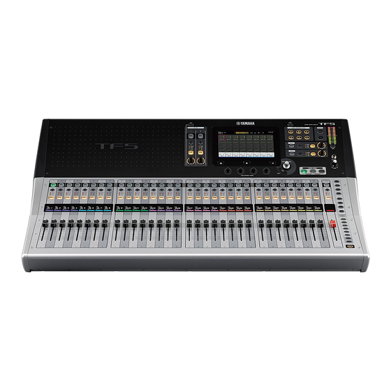
Page 5: Panel Layout
TF5/TF3/TF1 PANEL LAYOUT (パネルレイアウト) NOTE: 1. Top Panel(トップパネル) This illustration shows the top panel of the TF5. (イラストは TF5 のトップパネルです。 ) q Channel Strip section q チャンネルストリップセクション w ST IN (stereo input) section w ST IN(ステレオインプット)セクション e FX (effects) section e FX(エフェクト)セクション... - Page 6 TF5/TF3/TF1 2. Top Panel Details(トップパネル詳細) 2-1. Channel Strip section 2-2. ST IN (stereo input) section (チャンネルストリップセクション) (ST IN (ステレオインプッ ト)セクション) q [SEL] key w [CUE] key e Meter LEDs r [ON] key t Channel name display y Channel color indicator u Fader q [SEL] キー...
- Page 7 TF5/TF3/TF1 2-6. METER section 2-5. MUTE section (METER (メーター)セクション) (MUTE (ミュート)セクション) q [INPUT] key w [FX] key q Meter LEDs w [CLEAR] key q [INPUT] キー (CLEAR CUE key) w [FX] キー q メーター LED w [CLEAR] (CLEAR CUE)キー 2-7. PHONES section (PHONES (ヘッドフォン)セクション)...
- Page 8 TF5/TF3/TF1 2-11. Display section 2-12. STEREO/MASTER section (ディスプレイセクション) (STEREO/MASTER (ステレオマスター)セクション) q Display w Library key e Home key r Menu key t [TOUCH AND TURN] knob y [SHIFT] key u [USER DEFINED KNOBS] q ディスプレイ w ライブラリーキー e ホームキー r メニューキー...
- Page 9 2-13. iPad connector ( iPad 端子) 2-14. USB connector ( USB 端子) 3. Rear Panel(リアパネル) NOTE: This illustration shows the rear panel of the TF5. (イラストは TF5 のリヤパネルです。 ) q OMNI OUT jacks q OMNI OUT 端子 w ST IN jacks w ST IN 端子...
-
Page 10: Dimensions(寸法図
TF5/TF3/TF1 DIMENSIONS(寸法図) ● TF5 Unit ( 単位) : mm ● TF3 Unit ( 単位) : mm... - Page 11 TF5/TF3/TF1 ● TF1 Unit ( 単位) : mm...
-
Page 12: Tf5 Circuit Board Layout(Tf5 ユニットレイアウト
TF5/TF3/TF1 TF5 CIRCUIT BOARD LAYOUT(TF5 ユニットレイアウト) CONTROL PANEL ASSEMBLY 32 (コンパネ Ass’ y 32) CONTROL PANEL ASSEMBLY 32 (コンパネ Ass’ y 32) BOTTOM ASSEMBLY 32 (ボトム Ass’ y 32)... - Page 13 TF5/TF3/TF1 (ボトムAss’ y 32) HAAD HAAD HAAD HAAD SHIELD PS ASSEMBLY (シールド PS アッセンブリ) MAIN DC FAN MOTOR (DC ファンモーター) PSW CONNECTOR ASSEMBLY (PSW 束線) ACIN CONNECTOR ASSEMBLY LITHIUM BATTERY (ACIN 束線) (リチウム電池)...
- Page 14 TF5/TF3/TF1 <Rear view (背面) > ACIN CONNECTOR BOTTOM ASSEMBLY 32 ASSEMBLY (ボトム Ass’ y 32) (ACIN 束線) HAAD HAAD HAAD HAAD DC FAN MOTOR PSW CONNECTOR MAIN (DC ファンモーター) ASSEMBLY (PSW 束線) (コンパネAss’ y 32) FDPS FDPS PNFD8 FDPS PNFD8...
-
Page 15: Tf3 Circuit Board Layout(Tf3 ユニットレイアウト
TF5/TF3/TF1 TF3 CIRCUIT BOARD LAYOUT(TF3 ユニットレイアウト) CONTROL PANEL ASSEMBLY 24 (コンパネ Ass’ y 24) CONTROL PANEL ASSEMBLY 24 (コンパネ Ass’ y 24) BOTTOM ASSEMBLY 24 (ボトム Ass’ y 24)... - Page 16 TF5/TF3/TF1 (ボトムAss’ y 24) HAAD HAAD HAAD BRDG SHIELD PS ASSEMBLY (シールド PS アッセンブリ) MAIN DC FAN MOTOR (DC ファンモーター) PSW CONNECTOR ASSEMBLY (PSW 束線) ACIN CONNECTOR ASSEMBLY (ACIN 束線) LITHIUM BATTERY (リチウム電池)...
- Page 17 TF5/TF3/TF1 <Rear view (背面) > BOTTOM ASSEMBLY 24 ACIN CONNECTOR (ボトム Ass’ y 24) ASSEMBLY (ACIN 束線) BRDG HAAD HAAD HAAD DC FAN MOTOR PSW CONNECTOR MAIN (DC ファンモーター) ASSEMBLY (PSW 束線) (コンパネAss’ y 24) FDPS FDPS PNFD8 PNFD8 FDPS...
-
Page 18: Tf1 Circuit Board Layout(Tf1 ユニットレイアウト
TF5/TF3/TF1 TF1 CIRCUIT BOARD LAYOUT(TF1 ユニットレイアウト) CONTROL PANEL ASSEMBLY 16 (コンパネ Ass’ y 16) CONTROL PANEL ASSEMBLY 16 (コンパネ Ass’ y 16) BOTTOM ASSEMBLY 16 (ボトム Ass’ y 16)... - Page 19 TF5/TF3/TF1 (ボトムAss’ y 16) HAAD HAAD SHIELD PS ASSEMBLY (シールド PS アッセンブリ) MAIN DC FAN MOTOR (DC ファンモーター) PSW CONNECTOR ASSEMBLY (PSW 束線) ACIN CONNECTOR ASSEMBLY (ACIN 束線) LITHIUM BATTERY (リチウム電池)...
- Page 20 TF5/TF3/TF1 <Rear view (背面) > ACIN CONNECTOR BOTTOM ASSEMBLY 16 ASSEMBLY (ボトム Ass’ y 16) (ACIN 束線) HAAD HAAD DC FAN MOTOR PSW CONNECTOR MAIN (DC ファンモーター) ASSEMBLY (PSW 束線) (コンパネAss’ y 16) FDPS PNFD8 FDPS LCDC PNPS PNFD8 USBL...
-
Page 21: Tf5 Disassembly Procedure(Tf5 分解手順
TF5/TF3/TF1 TF5 DISASSEMBLY PROCEDURE(TF5 分解手順) Precautions (注意事項) Take care not to trap your fingers. 作業中は指を挟まない様に注意してください。 * Install the filament tape and the harness clamp in the same ※ フィラメントテープ、束線止めは、取り外す前と同じよ way as they were before removal. うに取り付けてください。 * Notes on Flat Cable ※... - Page 22 TF5/TF3/TF1 Side Pad R Assembly, Side Pad L Assembly (サイドパッドRアッセンブリ、サイドパッドLアッセンブリ) ..23 Control Panel Assembly 32 (コンパネ Ass'y 32) ....................... 23 Lithium Battery (リチウム電池) ..........................26 Disassembly Procedure of Bottom Assembly 32 (ボトム Ass'y 32 の分解) ............27 A-1. DA2 Circuit Board (DA2 シート) ..........................27 A-2.
- Page 23 TF5/TF3/TF1 Side Pad R Assembly, Side Pad L サイドパッド R アッセンブリ、 サイドパッ Assembly ド L アッセンブリ (所要時間:各約 1 分) (Time required: About 1 minute each) サイドパッド R アッセンブリ: Side Pad R Assembly : 1-1-1 [80A] のネジ 2 本を外して、サイドパッド R アッ...
-
Page 24: Bottom Assembly
TF5/TF3/TF1 CONTROL PANEL ASSEMBLY 32 (コンパネ Ass'y 32) SIDE PAD L ASSEMBLY (サイドパッド Lアッセンブリ) [30] [80B] [50] [40] [50] BOTTOM ASSEMBLY 32 (ボトム Ass'y 32) LITHIUM BATTERY (リチウム電池) [80A] SIDE PAD R ASSEMBLY (サイドパッド Rアッセンブリ) (サイドパッド Rアッセンブリとサイドパッド Lアッセンブリの外し方) * This figure is the SIDE PAD R ASSEMBLY. - Page 25 TF5/TF3/TF1 • Installing the Panel Stay(パネルステーの取り付け方) CONTROL PANEL ASSEMBLY 32 CONTROL PANEL ASSEMBLY 32 (コンパネ Ass'y 32) (コンパネ Ass'y 32) BOTTOM ASSEMBLY 32 BOTTOM ASSEMBLY 32 (ボトム Ass'y 32) (ボトム Ass'y 32) CONTROL PANEL ASSEMBLY 32 (コンパネ Ass'y 32) PANEL STAY (パネルステー)...
- Page 26 TF5/TF3/TF1 • Installing the Control Panel Assembly 32( の取り付け方) コンパネ Ass'y 32 CONTROL PANEL ASSEMBLY 32 BOTTOM ASSEMBLY 32 (コンパネ Ass'y 32) (ボトム Ass'y 32) CONTROL PANEL ASSEMBLY 32 CONTROL PANEL ASSEMBLY 32 (コンパネ Ass'y 32) (コンパネ Ass'y 32) Notch (切欠き)...
- Page 27 TF5/TF3/TF1 Disassembly Procedure of Bottom ボトム Ass'y 32 の分解 Assembly 32 A-1. DA2 シート (所要時間:約 9 分) A-1. DA2 Circuit Board A-1-1 サイドパッド R アッセンブリとサイドパッドL (Time required: About 9 minutes) アッセンブリを外します。 (1 項参照) A-1-1 Remove the side pad R assembly and side pad L A-1-2 コンパネ...
- Page 28 TF5/TF3/TF1 A-2. DA1 Circuit Board A-2. DA1 シート (所要時間:約 12 分) (Time required: About 12 minutes) A-2-1 サイドパッドRアッセンブリとサイドパッドL A-2-1 Remove the side pad R assembly and side pad L アッセンブリを外します。 (1 項参照) assembly. (See Procedure 1) A-2-2 コンパネ Ass'y 32 を固定します。 (2 項参照)...
- Page 29 TF5/TF3/TF1 A-3-6 HAAD (4) Circuit Board A-3-6 HAAD (4) シート (所要時間:約 15 分) (Time required: About 15 minutes) A-3-6-1 DA2 シートを外します。 (A-1 項参照) A-3-6-1 Remove the DA2 circuit board. (See procedure A-1) A-3-6-2 HAAD (3) シートを外します。 (A-3-5 項参照) A-3-6-2 Remove the HAAD (3) circuit board.
- Page 30 TF5/TF3/TF1 Remove the SHIELD PS ASSEMBLY. (シールド PSアッセンブリの外し方) <Top view (上面) > BOTTOM ASSEMBLY 32 SILICON PLATE B (ボトム Ass'y 32) [346] [240] (珪素鋼板プレート B) [390] SUPPORT ANGLE SHIELD PS ASSEMBLY (サポートアングル) (シールド PS アッセンブリ) <Rear view (背面) > [230]...
- Page 31 TF5/TF3/TF1 <Top view (上面) > BOTTOM ASSEMBLY 32 (ボトム Ass'y 32) [320] [310] [200] MAIN LITHIUM BATTERY (リチウム電池) <Rear view (背面) > [290] [295] BOTTOM ASSEMBLY 32 MAIN (ボトム Ass'y 32) Fig. 8 (図 8) OPT ANGLE ( OPT アングル)...
-
Page 32: Control Panel Assembly
TF5/TF3/TF1 A-5. PS Circuit Board A-5. PS シート (所要時間:約 18 分) (Time required: About 18 minutes) A-5-1 サイドパッドRアッセンブリとサイドパッドL A-5-1 Remove the side pad R assembly and side pad L アッセンブリを外します。 (1 項参照) assembly. (See Procedure 1) A-5-2 コンパネ Ass'y 32 を固定します。 (2 項参照)... - Page 33 TF5/TF3/TF1 A-6. DC Fan Motor A-6. DC ファンモーター (所要時間:約 17 分) (Time required: About 17 minutes) A-6-1 サイドパッドRアッセンブリとサイドパッドL A-6-1 Remove the side pad R assembly and side pad L アッセンブリを外します。 (1 項参照) assembly. (See Procedure 1) A-6-2 コンパネ Ass'y 32 を固定します。 (2 項参照)...
- Page 34 TF5/TF3/TF1 (上面) > ACIN CONNECTOR ASSEMBLY DC FAN MOTOR (DCファンモーター) (ACIN束線) [182] ACIN CONNECTOR ASSEMBLY (ACIN束線) (A視図) [140] [140] [140] Earth terminal (アース端子) Earth terminal (アース端子) Install the earth terminal of ACIN connector assembly in the direction shown in the drawing.
- Page 35 TF5/TF3/TF1 Disassembly Procedure of Control コンパネ Ass'y 32 の分解 Panel Assembly 32 B-1. LCDC シート (所要時間:約 7 分) B-1. LCDC Circuit Board B-1-1 サイドパッド R アッセンブリとサイドパッド L (Time required: About 7 minutes) アッセンブリを外します。 (1 項参照) B-1-1 Remove the side pad R assembly and side pad L B-1-2 コンパネ...
- Page 36 TF5/TF3/TF1 B-2. Crystal Display B-2. 液晶ディスプレイ (所要時間:約 7 分) (Time required: About 7 minutes) B-2-1 サイドパッド R アッセンブリとサイドパッド L B-2-1 Remove the side pad R assembly and side pad L アッセンブリを外します。 (1 項参照) assembly. (See Procedure 1) B-2-2 コンパネ Ass'y 32 を外します。 (2 項参照)...
- Page 37 TF5/TF3/TF1 B-3. PHN Circuit Board B-3. PHN シート (所要時間:約 7 分) (Time required: About 7 minutes) B-3-1 サイドパッド R アッセンブリとサイドパッド L B-3-1 Remove the side pad R assembly and side pad L アッセンブリを外します。 (1 項参照) assembly. (See Procedure 1) B-3-2 コンパネ...
- Page 38 TF5/TF3/TF1 B-5. PNC Circuit Board B-5. PNC シート (所要時間:約 11 分) (Time required: About 11 minutes) B-5-1 サイドパッド R アッセンブリとサイドパッド L B-5-1 Remove the side pad R assembly and side pad L アッセンブリを外します。 (1 項参照) assembly. (See Procedure 1) B-5-2 コンパネ...
- Page 39 TF5/TF3/TF1 B-6. PNL Circuit Board B-6. PNL シート (所要時間:約 7 分) (Time required: About 7 minutes) B-6-1 サイドパッド R アッセンブリとサイドパッド L B-6-1 Remove the side pad R assembly and side pad L アッセンブリを外します。 (1 項参照) assembly. (See Procedure 1) B-6-2 コンパネ...
- Page 40 TF5/TF3/TF1 B-8. FDPS (1–4) Circuit Board B-8. FDPS (1 ∼ 4) シート (所要時間 : 各約 6 分) (Time required: About 6 minutes each) B-8-1 サイドパッド R アッセンブリとサイドパッド L B-8-1 Remove the side pad R assembly and side pad L アッセンブリを外します。 (1 項参照)...
- Page 41 TF5/TF3/TF1 B-9. PNFD8 (1–4) Circuit Board, B-9. PNFD8 ( 1 ∼ 4) シート、 OLED ケースアッ OLED Case Assembly セイ B-9-1 Remove the side pad R assembly and side pad L B-9-1 サイドパッド R アッセンブリとサイドパッド L assembly. (See Procedure 1) アッセンブリを外します。 (1 項参照)...
- Page 42 TF5/TF3/TF1 B-10. PNFD1 Circuit Board B-10. PNFD1 シート (所要時間:約 7 分) B-10-1 サイドパッド R アッセンブリとサイドパッド L (Time required: About 7 minutes) B-10-1 Remove the side pad R assembly and side pad L アッセンブリを外します。 (1 項参照) assembly. (See Procedure 1) B-10-2 コンパネ Ass'y 32 を外します。 (2 項参照)...
- Page 43 TF5/TF3/TF1 B-11. PNF Circuit Board B-11. PNF シート (所要時間:約 7 分) (Time required: About 7 minutes) B-11-1 サイドパッド R アッセンブリとサイドパッド L B-11-1 Remove the side pad R assembly and side pad L アッセンブリを外します。 (1 項参照) assembly. (See Procedure 1) B-11-2 コンパネ Ass'y 32 を外します。 (2 項参照)...
-
Page 44: Tf3 Disassembly Procedure(Tf3 分解手順
TF5/TF3/TF1 TF3 DISASSEMBLY PROCEDURE(TF3 分解手順) Precautions (注意事項) Take care not to trap your fingers. 作業中は指を挟まない様に注意してください。 * Install the filament tape and the harness clamp in the same ※ フィラメントテープ、束線止めは、取り外す前と同じよ way as they were before removal. うに取り付けてください。 * Notes on Flat Cable ※... - Page 45 TF5/TF3/TF1 Side Pad R Assembly, Side Pad L Assembly (サイドパッドRアッセンブリ、サイドパッドLアッセンブリ) ..46 Control Panel Assembly 24 (コンパネ Ass'y 24) ....................... 46 Lithium Battery (リチウム電池) ..........................49 Disassembly Procedure of Bottom Assembly 24 (ボトム Ass'y 24 の分解) ............50 A-1. DA2 Circuit Board (DA2 シート) ..........................50 A-2.
- Page 46 TF5/TF3/TF1 Side Pad R Assembly, Side Pad L サイドパッド R アッセンブリ、 サイドパッ Assembly ド L アッセンブリ (所要時間:各約 1 分) (Time required: About 1 minute each) サイドパッド R アッセンブリ: Side Pad R Assembly : 1-1-1 [80A] のネジ 2 本を外して、サイドパッド R アッ...
- Page 47 TF5/TF3/TF1 CONTROL PANEL ASSEMBLY 24 (コンパネ Ass'y 24) [30] SIDE PAD L ASSEMBLY (サイドパッド Lアッセンブリ) [80B] [50] [40] [50] BOTTOM ASSEMBLY 24 (ボトム Ass'y 24) LITHIUM BATTERY (リチウム電池) [80A] SIDE PAD R ASSEMBLY (サイドパッド Rアッセンブリ) (サイドパッド Rアッセンブリとサイドパッド Lアッセンブリの外し方) * This figure is the SIDE PAD R ASSEMBLY.
- Page 48 TF5/TF3/TF1 • Installing the Panel Stay(パネルステーの取り付け方) CONTROL PANEL ASSEMBLY 24 CONTROL PANEL ASSEMBLY 24 (コンパネ Ass'y 24) (コンパネ Ass'y 24) BOTTOM ASSEMBLY 24 BOTTOM ASSEMBLY 24 (ボトム Ass'y 24) (ボトム Ass'y 24) CONTROL PANEL ASSEMBLY 24 (コンパネ Ass'y 24) PANEL STAY (パネルステー)...
- Page 49 TF5/TF3/TF1 • Installing the Control Panel Assembly 24( の取り付け方) コンパネ Ass'y 24 CONTROL PANEL ASSEMBLY 24 BOTTOM ASSEMBLY 24 (コンパネ Ass'y 24) (ボトム Ass'y 24) CONTROL PANEL ASSEMBLY 24 CONTROL PANEL ASSEMBLY 24 (コンパネ Ass'y 24) (コンパネ Ass'y 24) Notch (切欠き)...
- Page 50 TF5/TF3/TF1 Disassembly Procedure of Bottom ボトム Ass'y 24 の分解 Assembly 24 A-1. DA2 シート (所要時間:約 9 分) A-1. DA2 Circuit Board A-1-1 サイドパッド R アッセンブリとサイドパッドL (Time required: About 9 minutes) アッセンブリを外します。 (1 項参照) A-1-1 Remove the side pad R assembly and side pad L A-1-2 コンパネ...
- Page 51 TF5/TF3/TF1 A-2. DA1 Circuit Board A-2. DA1 シート (所要時間:約 12 分) (Time required: About 12 minutes) A-2-1 サイドパッドRアッセンブリとサイドパッドL A-2-1 Remove the side pad R assembly and side pad L アッセンブリを外します。 (1 項参照) assembly. (See Procedure 1) A-2-2 コンパネ Ass'y 24 を固定します。 (2 項参照)...
- Page 52 TF5/TF3/TF1 A-4. BRDG Circuit Board, MAIN Circuit Board A-4. BRDG シート、MAIN シート (Time required: About 15 minutes) (所要時間:約 15 分) A-4-1 Remove the side pad R assembly and side pad L A-4-1 サイドパッド R アッセンブリとサイドパッド L assembly. (See Procedure 1) アッセンブリを外します。...
- Page 53 TF5/TF3/TF1 Remove the SHIELD PS ASSEMBLY. (シールド PSアッセンブリの外し方) <Top view (上面) > SILICON PLATE B [346] [240] (珪素鋼板プレート B) [390] BOTTOM ASSEMBLY 24 (ボトム Ass'y 24) SUPPORT ANGLE SHIELD PS ASSEMBLY (サポートアングル) (シールド PS アッセンブリ) <Rear view (背面) > [230]...
- Page 54 TF5/TF3/TF1 <Top view (上面) > [320] [310] [200] MAIN BOTTOM ASSEMBLY 24 (ボトム Ass'y 24) LITHIUM BATTERY (リチウム電池) <Rear view (背面) > [290] [295] BOTTOM ASSEMBLY 24 MAIN (ボトム Ass'y 24) Fig. 8 (図 8) OPT ANGLE ( OPT アングル)...
- Page 55 TF5/TF3/TF1 A-5. PS Circuit Board A-5. PS シート (所要時間:約 17 分) (Time required: About 17 minutes) A-5-1 サイドパッドRアッセンブリとサイドパッドL A-5-1 Remove the side pad R assembly and side pad L アッセンブリを外します。 (1 項参照) assembly. (See Procedure 1) A-5-2 コンパネ Ass'y 24 を固定します。 (2 項参照)...
- Page 56 TF5/TF3/TF1 A-6. DC Fan Motor A-6. DC ファンモーター (所要時間:約 17 分) (Time required: About 17 minutes) A-6-1 サイドパッドRアッセンブリとサイドパッドL A-6-1 Remove the side pad R assembly and side pad L アッセンブリを外します。 (1 項参照) assembly. (See Procedure 1) A-6-2 コンパネ Ass'y 24 を固定します。 (2 項参照)...
- Page 57 TF5/TF3/TF1 (上面) > ACIN CONNECTOR ASSEMBLY DC FAN MOTOR (DCファンモーター) (ACIN束線) [182] ACIN CONNECTOR ASSEMBLY (ACIN束線) (A視図) [140] [140] [140] Earth terminal (アース端子) Earth terminal (アース端子) Install the earth terminal of ACIN connector assembly in the direction shown in the drawing.
- Page 58 TF5/TF3/TF1 Disassembly Procedure of Control コンパネ Ass'y 24 の分解 Panel Assembly 24 B-1. LCDC シート (所要時間:約 6 分) B-1. LCDC Circuit Board B-1-1 サイドパッド R アッセンブリとサイドパッド L (Time required: About 6 minutes) アッセンブリを外します。 (1 項参照) B-1-1 Remove the side pad R assembly and side pad L B-1-2 コンパネ...
- Page 59 TF5/TF3/TF1 B-2. Crystal Display B-2. 液晶ディスプレイ (所要時間:約 6 分) (Time required: About 6 minutes) B-2-1 サイドパッド R アッセンブリとサイドパッド L B-2-1 Remove the side pad R assembly and side pad L アッセンブリを外します。 (1 項参照) assembly. (See Procedure 1) B-2-2 コンパネ Ass'y 24 を外します。 (2 項参照)...
- Page 60 TF5/TF3/TF1 B-3. PHN Circuit Board B-3. PHN シート (所要時間:約 6 分) (Time required: About 6 minutes) B-3-1 サイドパッド R アッセンブリとサイドパッド L B-3-1 Remove the side pad R assembly and side pad L アッセンブリを外します。 (1 項参照) assembly. (See Procedure 1) B-3-2 コンパネ...
- Page 61 TF5/TF3/TF1 B-5. PNC Circuit Board B-5. PNC シート (所要時間:約 11 分) (Time required: About 11 minutes) B-5-1 サイドパッド R アッセンブリとサイドパッド L B-5-1 Remove the side pad R assembly and side pad L アッセンブリを外します。 (1 項参照) assembly. (See Procedure 1) B-5-2 コンパネ...
- Page 62 TF5/TF3/TF1 B-6. PNL Circuit Board B-6. PNL シート (所要時間:約 7 分) (Time required: About 7 minutes) B-6-1 サイドパッド R アッセンブリとサイドパッド L B-6-1 Remove the side pad R assembly and side pad L アッセンブリを外します。 (1 項参照) assembly. (See Procedure 1) B-6-2 コンパネ...
- Page 63 TF5/TF3/TF1 B-8. FDPS (1–3) Circuit Board B-8. FDPS (1 ∼ 3) シート (所要時間 : 各約 6 分) (Time required: About 6 minutes each) B-8-1 サイドパッド R アッセンブリとサイドパッド L B-8-1 Remove the side pad R assembly and side pad L アッセンブリを外します。 (1 項参照)...
- Page 64 TF5/TF3/TF1 B-9. PNFD8 (1–3) Circuit Board, B-9. PNFD8 ( 1 ∼ 3) シート、 OLED ケースアッ OLED Case Assembly セイ B-9-1 Remove the side pad R assembly and side pad L B-9-1 サイドパッド R アッセンブリとサイドパッド L assembly. (See Procedure 1) アッセンブリを外します。 (1 項参照)...
- Page 65 TF5/TF3/TF1 B-10. PNFD1 Circuit Board B-10. PNFD1 シート (所要時間:約 6 分) B-10-1 サイドパッド R アッセンブリとサイドパッド L (Time required: About 6 minutes) B-10-1 Remove the side pad R assembly and side pad L アッセンブリを外します。 (1 項参照) assembly. (See Procedure 1) B-10-2 コンパネ Ass'y 24 を外します。 (2 項参照)...
- Page 66 TF5/TF3/TF1 B-11. PNF Circuit Board B-11. PNF シート (所要時間:約 6 分) (Time required: About 6 minutes) B-11-1 サイドパッド R アッセンブリとサイドパッド L B-11-1 Remove the side pad R assembly and side pad L アッセンブリを外します。 (1 項参照) assembly. (See Procedure 1) B-11-2 コンパネ Ass'y 24 を外します。 (2 項参照)...
-
Page 67: Tf1 Disassembly Procedure(Tf1 分解手順
TF5/TF3/TF1 TF1 DISASSEMBLY PROCEDURE(TF1 分解手順) Precautions (注意事項) Take care not to trap your fingers. 作業中は指を挟まない様に注意してください。 * Install the filament tape and the harness clamp in the same ※ フィラメントテープ、束線止めは、取り外す前と同じよ way as they were before removal. うに取り付けてください。 * Notes on Flat Cable ※... - Page 68 TF5/TF3/TF1 Side Pad R Assembly, Side Pad L Assembly (サイドパッドRアッセンブリ、サイドパッドLアッセンブリ) ..69 Control Panel Assembly 16 (コンパネ Ass'y 16) ....................... 69 Lithium Battery (リチウム電池) ..........................72 Disassembly Procedure of Bottom Assembly 16 (ボトム Ass'y 16 の分解) ............73 A-1. DA2 Circuit Board (DA2 シート) ..........................73 A-2.
- Page 69 TF5/TF3/TF1 Side Pad R Assembly, Side Pad L サイドパッド R アッセンブリ、 サイドパッ Assembly ド L アッセンブリ (所要時間:各約 1 分) (Time required: About 1 minute each) サイドパッド R アッセンブリ: Side Pad R Assembly : 1-1-1 [80A] のネジ 2 本を外して、サイドパッド R アッ...
- Page 70 TF5/TF3/TF1 CONTROL PANEL ASSEMBLY 16 (コンパネ Ass'y 16) [30] SIDE PAD L ASSEMBLY (サイドパッド Lアッセンブリ) [80B] [50] [40] [50] BOTTOM ASSEMBLY 16 (ボトム Ass'y 16) LITHIUM BATTERY (リチウム電池) [80A] SIDE PAD R ASSEMBLY (サイドパッド Rアッセンブリ) (サイドパッド Rアッセンブリとサイドパッド Lアッセンブリの外し方) * This figure is the SIDE PAD R ASSEMBLY.
- Page 71 TF5/TF3/TF1 • Installing the Panel Stay(パネルステーの取り付け方) CONTROL PANEL ASSEMBLY 16 CONTROL PANEL ASSEMBLY 16 (コンパネ Ass'y 16) (コンパネ Ass'y 16) BOTTOM ASSEMBLY 16 BOTTOM ASSEMBLY 16 (ボトム Ass'y 16) (ボトム Ass'y 16) CONTROL PANEL ASSEMBLY 16 (コンパネ Ass'y 16) PANEL STAY (パネルステー)...
- Page 72 TF5/TF3/TF1 • Installing the Control Panel Assembly 16( の取り付け方) コンパネ Ass'y 16 CONTROL PANEL ASSEMBLY 16 BOTTOM ASSEMBLY 16 (コンパネ Ass'y 16) (ボトム Ass'y 16) CONTROL PANEL ASSEMBLY 16 CONTROL PANEL ASSEMBLY 16 (コンパネ Ass'y 16) (コンパネ Ass'y 16) Notch (切欠き)...
- Page 73 TF5/TF3/TF1 Disassembly Procedure of Bottom ボトム Ass'y 16 の分解 Assembly 16 A-1. DA2 シート (所要時間:約 8 分) A-1. DA2 Circuit Board A-1-1 サイドパッド R アッセンブリとサイドパッドL (Time required: About 8 minutes) アッセンブリを外します。 (1 項参照) A-1-1 Remove the side pad R assembly and side pad L A-1-2 コンパネ...
- Page 74 TF5/TF3/TF1 A-2. DA1 Circuit Board A-2. DA1 シート (所要時間:約 11 分) (Time required: About 11 minutes) A-2-1 サイドパッドRアッセンブリとサイドパッドL A-2-1 Remove the side pad R assembly and side pad L アッセンブリを外します。 (1 項参照) assembly. (See Procedure 1) A-2-2 コンパネ Ass'y 16 を固定します。 (2 項参照)...
- Page 75 TF5/TF3/TF1 A-4. MAIN Circuit Board A-4. MAIN シート (所要時間:約 17 分) (Time required: About 17 minutes) A-4-1 サイドパッド R アッセンブリとサイドパッド L A-4-1 Remove the side pad R assembly and side pad L アッセンブリを外します。 (1 項参照) assembly. (See Procedure 1) A-4-2 コンパネ...
- Page 76 TF5/TF3/TF1 Remove the SHIELD PS ASSEMBLY. (シールド PSアッセンブリの外し方) <Top view (上面) > SILICON PLATE B [346] (珪素鋼板プレート B) [240] [390] BOTTOM ASSEMBLY 16 (ボトム Ass'y 16) SUPPORT ANGLE SHIELD PS ASSEMBLY (サポートアングル) (シールド PS アッセンブリ) <Rear view (背面) > BOTTOM ASSEMBLY 16 (ボトム...
- Page 77 TF5/TF3/TF1 <Top view (上面) > [310] [320] [200] MAIN BOTTOM ASSEMBLY 16 (ボトム Ass'y 16) LITHIUM BATTERY (リチウム電池) <Rear view (背面) > [290] BOTTOM ASSEMBLY 16 (ボトム Ass'y 16) [295] MAIN Fig. 8 (図 8) OPT ANGLE ( OPT アングル)...
- Page 78 TF5/TF3/TF1 A-5. PS Circuit Board A-5. PS シート (所要時間:約 17 分) (Time required: About 17 minutes) A-5-1 サイドパッドRアッセンブリとサイドパッドL A-5-1 Remove the side pad R assembly and side pad L アッセンブリを外します。 (1 項参照) assembly. (See Procedure 1) A-5-2 コンパネ Ass'y 16 を固定します。 (2 項参照)...
- Page 79 TF5/TF3/TF1 A-6. DC Fan Motor A-6. DC ファンモーター (所要時間:約 16 分) (Time required: About 16 minutes) A-6-1 サイドパッドRアッセンブリとサイドパッドL A-6-1 Remove the side pad R assembly and side pad L アッセンブリを外します。 (1 項参照) assembly. (See Procedure 1) A-6-2 コンパネ Ass'y 16 を固定します。 (2 項参照)...
- Page 80 TF5/TF3/TF1 (上面) > ACIN CONNECTOR ASSEMBLY DC FAN MOTOR (DCファンモーター) (ACIN束線) [182] ACIN CONNECTOR ASSEMBLY (ACIN束線) (A視図) [140] [140] [140] Earth terminal (アース端子) Earth terminal (アース端子) Install the earth terminal of ACIN connector assembly in the direction shown in the drawing.
- Page 81 TF5/TF3/TF1 Disassembly Procedure of Control コンパネ Ass'y 16 の分解 Panel Assembly 16 B-1. LCDC シート (所要時間:約 6 分) B-1. LCDC Circuit Board B-1-1 サイドパッド R アッセンブリとサイドパッド L (Time required: About 6 minutes) アッセンブリを外します。 (1 項参照) B-1-1 Remove the side pad R assembly and side pad L B-1-2 コンパネ...
- Page 82 TF5/TF3/TF1 B-2. Crystal Display B-2. 液晶ディスプレイ (所要時間:約 5 分) (Time required: About 5 minutes) B-2-1 サイドパッド R アッセンブリとサイドパッド L B-2-1 Remove the side pad R assembly and side pad L アッセンブリを外します。 (1 項参照) assembly. (See Procedure 1) B-2-2 コンパネ Ass'y 16 を外します。 (2 項参照)...
- Page 83 TF5/TF3/TF1 B-3. PHN Circuit Board B-3. PHN シート (所要時間:約 5 分) (Time required: About 5 minutes) B-3-1 サイドパッド R アッセンブリとサイドパッド L B-3-1 Remove the side pad R assembly and side pad L アッセンブリを外します。 (1 項参照) assembly. (See Procedure 1) B-3-2 コンパネ...
- Page 84 TF5/TF3/TF1 B-5. PNC Circuit Board B-5. PNC シート (所要時間:約 10 分) (Time required: About 10 minutes) B-5-1 サイドパッド R アッセンブリとサイドパッド L B-5-1 Remove the side pad R assembly and side pad L アッセンブリを外します。 (1 項参照) assembly. (See Procedure 1) B-5-2 コンパネ...
- Page 85 TF5/TF3/TF1 B-6. PNL Circuit Board B-6. PNL シート (所要時間:約 6 分) (Time required: About 6 minutes) B-6-1 サイドパッド R アッセンブリとサイドパッド L B-6-1 Remove the side pad R assembly and side pad L アッセンブリを外します。 (1 項参照) assembly. (See Procedure 1) B-6-2 コンパネ...
- Page 86 TF5/TF3/TF1 B-8. FDPS (1–2) Circuit Board B-8. FDPS (1 ∼ 2) シート (所要時間 : 各約 5 分) (Time required: About 5 minutes each) B-8-1 サイドパッド R アッセンブリとサイドパッド L B-8-1 Remove the side pad R assembly and side pad L アッセンブリを外します。 (1 項参照)...
- Page 87 TF5/TF3/TF1 B-9. PNFD8 (1–2) Circuit Board, B-9. PNFD8 ( 1 ∼ 2) シート、 OLED ケースアッ OLED Case Assembly セイ B-9-1 Remove the side pad R assembly and side pad L B-9-1 サイドパッド R アッセンブリとサイドパッド L assembly. (See Procedure 1) アッセンブリを外します。 (1 項参照)...
- Page 88 TF5/TF3/TF1 B-10. PNFD1 Circuit Board B-10. PNFD1 シート (所要時間:約 6 分) B-10-1 サイドパッド R アッセンブリとサイドパッド L (Time required: About 6 minutes) B-10-1 Remove the side pad R assembly and side pad L アッセンブリを外します。 (1 項参照) assembly. (See Procedure 1) B-10-2 コンパネ Ass'y 16 を外します。 (2 項参照)...
- Page 89 TF5/TF3/TF1 B-11. PNF Circuit Board B-11. PNF シート (所要時間:約 6 分) (Time required: About 6 minutes) B-11-1 サイドパッド R アッセンブリとサイドパッド L B-11-1 Remove the side pad R assembly and side pad L アッセンブリを外します。 (1 項参照) assembly. (See Procedure 1) B-11-2 コンパネ Ass'y 16 を外します。 (2 項参照)...
-
Page 90: Lsi Pin Description(Lsi 端子機能表
TF5/TF3/TF1 LSI PIN DESCRIPTION(LSI 端子機能表) AK4396VF-E2 (X8324A00) DAC (Digital to Analog Converter) ............91 AM3352BZCZ60 (YF449B00) MICROPROCESSOR (MPU) ............92-93 CS4385A-DQZR (YF811A00) DAC (Digital to Analog Converter) ............95 CS5368-CQZR (X8488A00) ADC (Analog to Digital Converter) ............91 GL852G-MNG03 (YC486A00) USB 2.0 MTT HUB CONTROLLER ............97 LAN8720A-CP-TR (YF905A00) ETHERNET TRANSCEIVER (PHY).......... - Page 91 TF5/TF3/TF1 CS5368-CQZR (X8488A00) ADC (Analog to Digital Converter) HAAD (HACOM): IC903 NAME FUNCTION NAME FUNCTION AIN2+ Differential Analog– Audio signals are LRCK/FS Serial Audio Channel Clock– In I S Mode, AIN2- presented differently to the delta sigma Serial Audio Channel Select. When low, the modulators via the AIN+/- pins.
- Page 92 TF5/TF3/TF1 AM3352BZCZ60 (YF449B00) MICROPROCESSOR (MPU) MAIN (MAINCOM): IC905 Outer Outer Name Function Name Function 82 E10 VDDSHV6 VCC VDD for I/O GND GND 83 E11 VDDSHV6 VCC VDD for I/O A2 VDD_MPU_MON Voltage Monitor Input(Not Used) RESERVED Not Used 84 E12...
- Page 93 TF5/TF3/TF1 Outer Outer Name Function Name Function 163 K1 DDR_D9 BIDIRECT DDR SDRAM DATA INPUT/OUTPUT 244 P10 VDDSHV2 VCC VDD for I/O 164 K2 DDR_D10 BIDIRECT DDR SDRAM DATA INPUT/OUTPUT 245 P11 VDDSHV2 VCC VDD for I/O 165 K3 DDR_D11...
- Page 94 TF5/TF3/TF1 SN75LVDS84ADGGR (X4212A0R) LVDS TRANSMITTERS MAIN (MAINCOM): IC916 NAME FUNCTION NAME FUNCTION Data bus Data bus Power supply CLKIN Input clock for CLKIN MIDI SHTDN Data bus PLLGND Ground Ground PLLV Power supply PLLGND Data bus Goround LVDSGND Power supply...
- Page 95 TF5/TF3/TF1 DA1 (DACOM): IC004 CS4385A-DQZR (YF811A00) DAC (Digital to Analog Converter) DA2: IC002 NAME FUNCTION NAME FUNCTION DSDA2 Quiescent Voltage - Filter connection for internal quiescent voltage. DSDB1 Direct Stream Digital Input - Input for Direct MUTEC234 Mute Control Stream Digital serial audio data.
- Page 96 TF5/TF3/TF1 MB9AF132LAPMC1 (YF746B00) MICROCONTROLLER (MCU) HAAD (HACOM): IC902 NAME FUNCTION NAME FUNCTION Power supply AVCC A/D converter analog power pin AVRH A/D converter analog reference voltage input General-purpose I/O port 5 pin. AVSS A/D converter GND pin SDA2_2 Multi-function serial interface ch.2 output pin.
- Page 97 TF5/TF3/TF1 GL852G-MNG03 (YC486A00) USB 2.0 MTT HUB CONTROLLER USBR (MAINCOM): IC002 NAME FUNCTION NAME FUNCTION AVDD Analog power supply +3.3 V SEL48# Digital power supply +3.3 V AGND Analog ground RESET# External reset input TEST Test signal USB signals for USPORT...
- Page 98 TF5/TF3/TF1 PNFD8 (PNFDCOM): IC002 M36BFYFG-7PP4(DBB) (YG822A00) MICROCONTROLLER (MCU) PNC (PNCOM): IC003 NAME NAME FUNCTION IC002 IC002 IC003 I/O Input/Output port FDPOS4 AIN4 Analog input I/O Input/Output port FDPOS5 AIN5 Analog input I/O Input/Output port FDPOS6 AIN6 Analog input I/O Input/Output port...
- Page 99 TF5/TF3/TF1 NAME NAME FUNCTION IC002 IC002 IC003 I/O Input/Output port FDA1 I/O Address data bus pin TXD4 UART transmit pin IROUT4 lrDA1.0 transmit pin I/O Input/Output port FDA2 I/O Address data bus pin RXD4 UART receive pin IRIN4 lrDA1.0 receive pin...
- Page 100 TF5/TF3/TF1 NAME NAME FUNCTION IC002 IC002 IC003 I/O Input/Output port C/D/C Chip select pin Output SP2DI SSP data input pin /GEMG3 Multi-purpose timer read strobe pin (IGBT mode) abnormal status detection input INT7 External interrupt pin I/O Input/Output port /CRES...
- Page 101 TF5/TF3/TF1 NAME NAME FUNCTION IC002 IC002 IC003 I/O Input/Output port /UVLO /UVLO(INT2) INT2 External interrupt pin MT1IN Multi-purpose timer (IGBT mode) input pin /ADTRG External activation pin for AD converter I/O Input/Output port LCDEN2 /GEMG1 Multi-purpose timer (IGBT mode) abnormal status detection input...
- Page 102 TF5/TF3/TF1 TPS65910AA1RS (YF900A00) POWER MANAGEMENT IC MAIN (MAINCOM): IC903 NAME FUNCTION NAME FUNCTION PWRHOLD Switch-on/-off control signal VPLL LDO regulator output VMMC LDO regulator output TESTV Analog test output (DFT) VCC3 VMMC VAUX33 power input BOOT0 Power-up sequence selection VAUX33...
- Page 103 TF5/TF3/TF1 LCMXO2280C-3TN144C (YG282A00) CPLD (Complex Programmable Logic Device) MAIN (MAINCOM): IC802 NAME FUNCTION NAME FUNCTION User programmable pin RESERVE User programmable pin User programmable pin EXTWC[1] User programmable pin BID[0] User programmable pin RESERVE User programmable pin /WRH User programmable pin...
- Page 104 TF5/TF3/TF1 PIC32MX470F512H-I (YG283B00) MICROCONTROLLER (MCU) MAIN (MAINCOM): IC651 NAME FUNCTION NAME FUNCTION RP_E RPE5 SDI2 (SDI2R=0110) (SD2in) USBID USB OTG ID Detect GPIO_E NC (LOW) VBUS VBUS USB Bus Power Monitor GPIO_E NC (LOW) +3.3D VUSB3V3 USB internal transceiver supply.
- Page 105 TF5/TF3/TF1 LPC812M101JDH20J (YG479A00) MICROCONTROLLER (MCU) MAIN (MAINCOM): IC854 NAME FUNCTION NAME FUNCTION PIO0_17 PIO0_15 General purpose digital input/output pin. PIO0_13 General purpose digital input/output pin. PIO0_1/ General purpose digital input/output pin./Analog PIO0_12 ACMP_2/ comparator input 2./External clock input./In RESET/ External reset input: A LOW-going pulse as short CLKIN/ boundary scan mode: TDI (Test Data In).
-
Page 106: Circuit Boards(シート基板図
TF5/TF3/TF1 CIRCUIT BOARDS(シート基板図) BRDG (HACOM) Circuit Board (YF862D0) (TF3 only) ......115 DA1 (DACOM) Circuit Board (YF860C0) ..........112 DA2 Circuit Board (YF861C0) ..............113 FDPS (PNFDCOM) Circuit Board (YF863D0) ........124 HAAD (HACOM) Circuit Board (YF862D0) ........114/115 LCDC (PNCOM) Circuit Board (YF864D0)..........107 MAIN (MAINCOM) Circuit Board (YF859C0) ........108/110... - Page 107 TF5/TF3/TF1 LCDC (PNCOM) Circuit Board to CRYSTAL DISPLAY (液晶ディスプレイ) to CRYSTAL DISPLAY (液晶ディスプレイ) to PNPS-CN504 to PNC-CN004 to MAIN-CN904 to PNC-CN009 Component side (部品側) Pattern side (パターン側) 2NA-ZJ06380...
- Page 108 TF5/TF3/TF1 MAIN (MAINCOM) Circuit Board (リチウム電池) Battery VN103500 Battery WR846000 (Battery holder for VN103500) Notice for back-up battery removal. Push the battery as shown in figure, then the battery will pop up. Druk de batterij naar beneden zoals aangeven in de tekening, de batterij springt dan naar voren.
- Page 109 TF5/TF3/TF1 Scale: 90/100 (リチウム電池) A’ Component side (部品側) 2NA0-ZJ06330...
- Page 110 TF5/TF3/TF1 MAIN (MAINCOM) Circuit Board B’ 2NA0-ZJ06330...
- Page 111 TF5/TF3/TF1 Scale: 90/100 B’ Pattern side (パターン側) 2NA0-ZJ06330...
- Page 112 TF5/TF3/TF1 DA1 (DACOM) Circuit Board Component side (部品側) 2NA-ZJ06450...
- Page 113 TF5/TF3/TF1 Scale: 90/100 DA2 Circuit Board Component side (部品側) 2NA-ZJ06430...
- Page 114 TF5/TF3/TF1 Scale: 85/100 HAAD (HACOM) Circuit Board CN901 CN907 TF5/3/1 HAAD(1) HAAD(2) HAAD(3) HAAD(4) Component side (部品側) HAAD(1) HAAD(2) HAAD(3) HAAD(4) Installed Installed Installed Installed Installed Installed Installed Not installed Installed Installed Not installed Not installed 2NA-ZJ06440...
- Page 115 TF5/TF3/TF1 Scale: 85/100 HAAD (HACOM) Circuit Board Pattern side (パターン側) BRDG (HACOM) Circuit Board Scale: 85/100 Component side (部品側) Pattern side (パターン側) BRDG, HAAD: 2NA-ZJ06440...
- Page 116 TF5/TF3/TF1 PS Circuit Board C’ 2NA-ZJ06320...
- Page 117 TF5/TF3/TF1 C’ Component side (部品側) 2NA-ZJ06320...
- Page 118 TF5/TF3/TF1 PNPS (PNCOM) Circuit Board Component side (部品側) Pattern side (パターン側) PNC (PNCOM) Circuit Board D’ PNC, PNPS: 2NA-ZJ06380...
- Page 119 TF5/TF3/TF1 Component side (部品側) Component side (部品側) D’ 2NA-ZJ06380...
- Page 120 TF5/TF3/TF1 PNC (PNCOM) Circuit Board E’ 2NA-ZJ06380...
- Page 121 TF5/TF3/TF1 PHN (DACOM) Circuit Board to DA1-CN901 to PHONES Component side (部品側) E’ Pattern side (パターン側) PNC: 2NA-ZJ06380 PHN: 2NA-ZJ06450...
- Page 122 TF5/TF3/TF1 PNFD8 (PNFDCOM) Circuit Board PNFD8(1) PNFD8(2) PNFD8(3) PNFD8(4) Installed Installed Installed Installed Installed Installed Installed Not installed Installed Installed Not installed Not installed Component side (部品側) 2NA-ZJ81690...
- Page 123 TF5/TF3/TF1 PNFD8 (PNFDCOM) Circuit Board PNFD8(1): N.C. CN003 CN005 CN004 CN006 CN317 CN318 TF5/3/1 PNFD8(1) PNFD8(2) TF5/3/1 PNFD8(1) PNFD8(2) TF5/3/1 PNFD8(1) PNFD8(2) TF5/3 PNFD8(2) PNFD8(3) TF5/3 PNFD8(2) PNFD8(3) TF5/3 PNFD8(2) PNFD8(3) PNFD8(3) PNFD8(4) PNFD8(3) PNFD8(4) PNFD8(3) PNFD8(4) Pattern side (パターン側)...
- Page 124 TF5/TF3/TF1 FDPS (PNFDCOM) Circuit Board FDPS(1) FDPS(2) FDPS(3) FDPS(4) Installed Installed Installed Installed Installed Installed Installed Not installed Installed Installed Not installed Not installed Component side (部品側) Pattern side (パターン側) 2NA-ZJ81690...
- Page 125 TF5/TF3/TF1 USBL (MAINCOM) Circuit Board to PS-CN310 to MAIN-CN652 (iPad) Component side (部品側) Pattern side (パターン側) USBR (MAINCOM) Circuit Board to PS-CN311 (DATA) to MAIN-CN905 Pattern side (パターン側) Component side (部品側) USBL, USBR: 2NA0-ZJ06330...
- Page 126 TF5/TF3/TF1 PNF (PNCOM) Circuit Board Component side (部品側) PNFD1 (PNCOM) Circuit Board Component side (部品側) Component side (部品側) Pattern side (パターン側) PNF, PNFD1: 2NA-ZJ06380...
- Page 127 TF5/TF3/TF1 PNF (PNCOM) Circuit Board Pattern side (パターン側) PNL (PNCOM) Circuit Board Component side (部品側) to PNC-CN005 Pattern side (パターン側) PNF, PNL: 2NA-ZJ06380...
-
Page 128: Test Program(テストプログラム
TF5/TF3/TF1 TEST PROGRAM Preparation Activating TF5, TF3, or TF1 in test program mode will change the settings and parameters in TF5, TF3, and TF1, enabling tests of the TF series. Measurement Environment Normal Temperature: 5 to 40 degree, Normal Humidity: 30 to 90% Note) The following measurement conditions are permitted if the measurement result is in the inspection standard. - Page 129 TF5/TF3/TF1 • Connection diagram for checking iPad USB Memory IPOD_CONNECT USB Memory USB_CONNECT TO HOST USB PC (Win 7) ETHER, TO_HOST_PC Ethernet Foot SW OMNI OUT 1 OMNI OUT 8 OMNI OUT 9 OMNI OUT 16 INPUT 1 INPUT 16...
- Page 130 TF5/TF3/TF1 Operation method outline 6-1. Operation by GUI of TF main part • Starting the test program A power supply is started pushing [A] switch and [F] switch of "USER DEFINED KEYS". After that, wait until the test screen starts.
- Page 131 ----- V1.00 V1.00 w [MAC address] display The MAC address of a Network connector is displayed. Un-writing in and when inaccurate (the vendor ID section is not YAMAHA), it is displayed as "--:--:--:--:--:--". e [IP address] display IP MAC address is displayed.
- Page 132 TF5/TF3/TF1 S Each inspection screen If each inspection screen is started from the starting screen, the screen as shown in the above fi gure will be displayed. (The above fi gure is an example of product inspection screen.) Push the [PLAY] button to start the automatic inspection sequence. After that operate the mixer according to direction of the screen.
- Page 133 TF5/TF3/TF1 S Inspection item part Check box Item button Result display They are a check box, and item button, and a result display from the left. [Check box] Push the check box to add (White) or delete (Gray) to the sequence of the desired item is performed.
- Page 134 TF5/TF3/TF1 eDisplay of inspection log In the case of semiautomatic judging Operate switches on sheet PNL. PASS : RTC USB_CONNECT ABORT PASS : USB_CONNECT PASS : FSW In an inspection which judges by detecting operation of ETHER handlers, such as the inspection of switches, the popup...
- Page 135 TF5/TF3/TF1 6-2. Product type initialization Command Clear Product type by sending serial command “PRODUCT_UNKNOWN” to TF using PC communication software (ex: TeraTerm). The following settings are necessary in order to send commands. 6-2-1. Network setting 6-2-3. Supplemental Setup After starting normally, a Network setup can be set up as It is necessary to make the IP address of PC into a fi...
- Page 136 PNFD_CONNECT ○ – CPU PORT FOOT SWITCH connection check Semi Auto ○ – Foot switch (YAMAHA FC4 or jig ※ ) is required. Ether cuircuit check Manual ETHER ○ – PC and Ethernet cable are required. Battery voltage check Auto BATT ○...
- Page 137 Auto DSP_I2C ○ – USB TO HOST terminal connection check Semi Auto USB_TO_HOST ○ – A PC installed with Yamaha Steinberg USB Driver, and a USB cable are required. PIC connection check Auto PIC_CONNECT ○ – MFI connection check Auto MFI_CONNECT ○...
- Page 138 TF5/TF3/TF1 Description Judge- MEAS- Item Sub Item TOTAL ment UREMEN Remarks Leds on PNL circuit board check Manual LED_PNL – ○ Leds on PNC circuit board check Manual LED_PNC ○ – Leds on PNFD1 circuit boardcheck Manual LED_PNFD1 ○ –...
- Page 139 TF5/TF3/TF1 Each Inspection Item 7-1-3. VER_MAIN 7-1. VERSION [Contents] The version of the main program is inspected. [Procedure] <GUI> MAIN Program is Vx.xx ? FAIL PASS Popup dialog as shown in the above fi gure is displayed on the screen. Judge whether it is same as the version described.
- Page 140 Popup dialog as shown in the above fi gure is displayed on Popup dialog as shown in the above fi gure is displayed on the the screen; it checked the product type (TF5/TF3/TF1) screen. Judge whether it is same as the version described.
- Page 141 TF5/TF3/TF1 7-2. CPU PORT 7-2-3. PNC_CONNECT [Contents] Inspect the connection between PNC circuit board and CPU (IC905). [Procedure] <GUI> Automatic judgment <Display of inspection log> In the case of PASS, “PASS: PNC_CONNECT”. In the case of FAIL, “FAIL: PNC_CONNECT”. 7-2-4. PNFD_CONNECT The example of a screen of the product test.
- Page 142 TF5/TF3/TF1 7-3. CPLD 7-2-6. ETHER [Contents] Inspect the connection between Ether circuit and CPU(IC905). [Procedure] <GUI> Connection of ETHER established? FAIL PASS Since popup dialog as shown in the above fi gure is displayed When you conduct the following inspections after these...
- Page 143 TF5/TF3/TF1 7-3-3. CPLD_MUTE 7-4. SLOT [Contents] Inspect the connection of MUTEOUT[1][2] port of CPLD and DSP#1-#5 and PIC. [Procedure] <GUI> Automatic judgment <Display of inspection log> In the case of PASS, “PASS: CPLD_MUTE”. In the case of FAIL, the contents of failure are returned like “FAIL: IC101(T10) IC101(B10)”.
- Page 144 TF5/TF3/TF1 7-5. DSP 7-5-2. DSP_PORT [Contents] Inspect the signal routes of GPIO between CPU(IC905) and DSP#1-5(IC101, IC201, IC301, IC401, IC501). [Procedure] <GUI> Automatic judgment <Display of inspection log> In the case of PASS, “PASS: DSP_PORT”. In the case of FAIL, the contents of failure are returned like “FAIL: DSP_PORT IC101 IC201 IC301 IC401 IC501”.
- Page 145 TF5/TF3/TF1 DSP15 SDIO connections from DSP#1(IC101) to 7-5-4. DSP_SDRAM DSP#5(IC501). [Contents] – > IC501(T3) IC101(T3) Inspect the connections of SDRAM interface between – > IC501(R2) IC101(R2) DSP#1-5(IC101, IC201, IC301, IC401, IC501) and each DSP23 SDIO connections from DSP#2(IC201) to SDRAM.
- Page 146 DSP#5(IC501) and USB TO HOST connector (CN602). CPU(IC651) and Authentication Coprocessor(IC652). Determined by detecting connection with the PC. IC651(30/31/32)< – >IC652(7/2/6) [Procedure] [Procedure] Prepare a PC which installed Yamaha Steinberg USB Driver <GUI> in advance. Automatic judgment <GUI> <Display of inspection log>...
- Page 147 OMNI OUT 1 – > INPUT 1, Inspect the signal routes of /MUTE_MFI, MUTE_OUT[2] OMNI OUT 8 – > INPUT16, and IRQ_MFI. OMNI OUT 9 – > INPUT17 (Used in TF5 or TF3), [Procedure] OMNI OUT16 – > INPUT32 (Used in TF5), <GUI>...
- Page 148 TF5/TF3/TF1 HAAD22 AXR0[7](A6) of DSP#4(IC401) – > 7-8. LCD OMNI1-8(11 ) of CN705 ) of CN702 – > SD_HA2(6 AXR2[1](B7) of DSP#2(IC201) HAAD31 AXR0[8](B6) of DSP#4(IC401) – > OMNI9-16(13 ) of CN705 ) of CN703 – > SD_HA3(6 AXR2[2](A7) of DSP#1(IC101) HAAD32 AXR0[8](B6) of DSP#4(IC401) –...
- Page 149 TF5/TF3/TF1 3) Gradation 7-8-2. BACKLIGHT [Contents] Inspect the backlight circuit of LCD. [Procedure] <GUI> LCD Backlight Diag Result FAIL PASS Popup dialog as shown in the above fi gure is displayed on the screen. Judge whether the brightness of the backlight of the 4) White, 5) Red, 6) Green, 7) Blue, 8) Black fill each LCD is changing and select [PASS] or [FAIL].
- Page 150 Although the target of the inspection replaces CH9-16, CH17-24 or CH25-32, the contents are the same as that of “7-9-1. CH_NAME_1”. “7-9-3. CH_NAME_3” function is for TF5 and TF3. “7-9-4. CH_NAME_4” function is for TF5 only. 7-10. SWITCH The example of a screen of the product test.
- Page 151 Although the target of the inspection replaces CH9-16, it, push the [ABORT] button. Close the popup dialog. CH17-24 or CH25-32, the contents are the same as that of “7-10-5. SW_FD8_1”. “7-10-7. SW_FD8_3” function is for TF5 and TF3. “7-10-8. SW_FD8_4” function is for TF5 only.
- Page 152 TF5/TF3/TF1 7-11. ALL LED 7-11-3. RED_LEDS [Contents] Inspect whether all the red LEDs are simultaneously on. [Procedure] <GUI> ALL red LEDs light? FAIL PASS The procedure is the same as “7-11-2. ORANGE_LEDS”. The example of a screen of the product test.
- Page 153 TF5/TF3/TF1 7-12. LED 7-12-2. LED_PNC [Contents] Inspect the LEDs on the PNC circuit board. [Procedure] <GUI> Check LEDs on sheet PNC. FAIL PASS The procedure is the same as “7-12-1. LED_PNL”. The example of a screen of the product test.
- Page 154 Although the target of the inspection replaces CH9-16, CH17-24 or CH25-32, the contents are the same as that of Check LEDs on sheet PNF. “7-12-5. LED_FD8_1”. “7-12-7. LED_FD8_3” function is for TF5 and TF3. FAIL PASS “7-12-8. LED_FD8_4” function is for TF5 only."...
- Page 155 TF5/TF3/TF1 The following LEDs turn on for the target encoders. If 7-13. ENCODER operation is detected, LEDs will turn off. UDEF KNOB A – > METER -25 UDEF KNOB B – > METER -30 UDEF KNOB C – > METER -40 UDEF KNOB D –...
- Page 156 INPUT17-24 or INPUT25-32, the contents are the same as ● Take measurements with these settings, according to that of “7-15-1. HA_HGAIN_1”. “7-15-3. HA_HGAIN_3” function is for TF5 and TF3. TEST SPEC “A. INPUT-OMNI OUT Gain max.”. (See page 159.) When measurement is completed, push “7-15-4.
- Page 157 TF5/TF3/TF1 7-16-2. HAAD34_MAX (INPUT) [Procedure] Push the [HAAD12_MIN] button in the MEASUREMENT [Contents] SETTING screen. TF becomes the setup mentioned above The signals inputted into INPUT17-32 are outputted to and the following popup dialog is displayed. OMNI OUT 1-16. The HA GAIN setting at that time is +66dB.
- Page 158 TF5/TF3/TF1 7-16-6. HAAD_48V_ON (+V48) 7-16-5. STIN (INPUT) In order to measure the Phantom Power Supply, set +48V for [Contents] all channels to ON. The signals inputted into ST IN 1-2 are outputted to OMNI (● TEST SPEC “F. Phantom Power Supply”...
- Page 159 1kHz -62dBu OMNI OUT 1-16 T h e d i ff e r e n c e i n t h e l e v e l INPUT 17-32 (TF5) Gain Test Command : between channels shall be 2dB or...
-
Page 160: Settings For Shipment(出荷設定
≦ -23 dBu F. Phantom Power Supply This measurement can be represented by following INPUT channel. TF5 : INPUT 1,9,17,25 TF3 : INPUT 1,9,17 TF1 : INPUT 1,9 Connect load resistance 10kΩ between pin No.1 and 2. Short pin No.2 and 3 with 0Ω. - Page 161 電圧 周波数 100V-10% to 230V+10% 50 or 60Hz 必要機材 ・ TF5/TF3/TF1 本体(検証対象) ・ PC(Yamaha Steinberg USB Driver インストール済み) (ETHER テスト、USB_TO_HOST テスト、コマンド送 信時に使用) ・ Ethernet ケーブル(ETHER テスト、コマンド送信時に使用) ・ USB メモリー(USB_CONNECT、IPOD_CONNECT で使用) ・ USB ケーブル(USB_TO_HOST テストで使用) ・ フットスイッチ(YAMAHA FC4 または治具) (FSW テストで使用)...
- Page 162 TF5/TF3/TF1 ● 検査接続図 iPad USB Memory IPOD_CONNECT USB Memory USB_CONNECT TO HOST USB PC (Win 7) ETHER 、 TO_HOST_PC Ethernet Foot SW OMNI OUT 1 OMNI OUT 8 OMNI OUT 9 OMNI OUT 16 INPUT 1 INPUT 16 AIN/AOUT INPUT 17 ※...
- Page 163 TF5/TF3/TF1 操作方法概要 6-1. TF 本体 GUI での操作 ・ テストプログラムの起動 「USER DEFINED KEYS」の[A]スイッチと [F] スイッチを約 30 秒間押しながら電源を起動します。 その後、テスト画面が起動するまで待ってください。 ・ 基本操作方法 [TOUCH AND TURN]ノブを回すことよって画面内のボタンを選択し、 [TOUCH AND TURN]ノブを押すこと で実行します。 あるいは、画面内のボタンを直接タッチすることで選択または実行します。 USER DEFINED KEYS [A] スイッチ [F] スイッチ [TOUCH AND TURN] ノブ ・ 本体 GUI 操作方法...
- Page 164 : ----- ----- V1.00 V1.00 w[MAC address] display ネットワーク端子の MAC アドレスを表示します。 未書込みや、不正な ( ベンダー ID 部がヤマハで無い)場合は“--:--:--:--:--:--”と表示します。 e[IP address] display IP アドレスを表示します。 r[Product type] display 機種タイプを表示します。 (TF5/TF3/TF1) 機種タイプが未設定の場合は、 “ --- ”と表示します。 t[TOTAL] button 総合検査用の画面が起動します。 y[MAINCOM] button MAINCOM シート検査用の画面が起動します。 u[HACOM] button HACOM シート検査用の画面が起動します。...
- Page 165 TF5/TF3/TF1 ●各検査画面 起動画面から各検査画面を起動すると、上図のような画面を表示します。 (上図は総合検査画面の例) 基本的に[PLAY]ボタンを押すと、自動検査のシーケンスがスタートするので、画面の指示に従って操作を 行います。 検査が完了すると、画面の左上に総合判定が「PASS」または「FAIL」を表示します。 q総合判定表示 tトランスポートボタン 検査全体の総合結果を「PASS」または「FAIL」で 表示を行います。 自動検査シーケンスの操作を行います。 [PLAY]ボタンを押すと自動シーケンスがスタート します。 w [CLOSE]ボタン 自動検査シーケンス中は、ボタンが下記のようにな ります。 各検査画面を終了し、起動画面に戻ります。 「USER DEFINED KEYS」 [B]を押すことでも代用 シーケンスを中断する場合は、 [PAUSE]ボタンを できます。 押します。 中断中は、ボタンが下記のようになります。 e項目選択マクロボタン シーケンスを再開する場合は、 [PLAY]ボタンを押 [ALL] すべての項目を検査対象とします。 します。 [CLEAR] すべての項目を検査対象外とします。 シーケンスを終了する場合は、 [STOP]ボタンを押 [DEFAULT] 検査対象の選択を初期値に戻します。...
- Page 166 TF5/TF3/TF1 ●検査項目部分 チェックボックス 項目ボタン 結果表示 左から、チェックボックス、項目ボタン、結果表示となります。 [チェックボックス] 該当項目のチェックボックスを押し、自動検査のシーケンスに追加(白色) /削除(灰色)を行います。 [項目ボタン] 該当項目ボタンを押すと、その項目の個別検査を実行します。 [結果表示] 該当項目の検査結果の合否を表示します。 表示される項目は全検査で共通です。 検査は可能ですが、必須でない項目は起動時にチェックが外れた状態になります。 該当検査では検査できない項目は、グレーアウト表示され操作できません。 各検査項目画面 各検査項目を実行しているときには上図のような画面を表示します。 自動シーケンス実行中の場合は、画面が自動でオープンし、右に表示されている項目が自動的に実行され、終 了すると自動でクローズします。 個別に起動された場合は、 [PLAY]ボタンを押すと、右に表示されている項目を上から順番に実行します。 w[CLOSE]ボタン q判定表示 全体の結果を「PASS」または「FAIL」で表示を行 います。 項目画面を終了し、検査画面に戻ります。 「USER DEFINED KEYS」 [B]を押すことでも代用 できます。...
- Page 167 TF5/TF3/TF1 e検査ログ表示 半自動判定の場合 Operate switches on sheet PNL. PASS : RTC USB_CONNECT ABORT PASS : USB_CONNECT PASS : FSW スイッチの検査など、 本体操作子の操作の検出を行っ ETHER PASS : ETHER て判定する検査は、上図のようなポップアップを表 BATTERY 示します。 PASS : BATTERY 表示されている操作をすべて検出した場合、検査に PASS し、ポップアップを自動で閉じます。 検査の実行内容および結果の詳細を表示します。 すべての操作を行った後、ポップアップが閉じない 場合は FAIL です。 [ABORT]ボタンを押すと、 ポッ...
- Page 168 TF5/TF3/TF1 6-2. プロダクトタイプ初期化コマンド PC の通信ソフトウェア(例:TeraTerm)を使ってシリアルコマンド「PRODUCT_UNKNOWN」を TF に送信するこ とでプロダクトタイプをクリアします。 コマンドを送信するためには以下の設定が必要です。 6-2-1. TF シリーズのネットワーク設定 6-2-3. 補足設定 TF シリーズを通常起動した後、TF 本体のネット PC を固定 IP アドレスにする必要があります。 ワークを以下のように設定します。 以下に WindowsPC での設定例を示します。 [1]TCP/IPv4 のプロパティを開きます。 IP Address = 192. 168. Subnet Mask = 255. 255. 255. Gateway = 255.
- Page 169 自動 ○ PNFD_CONNECT PNFD8 シートと CPU の I2C 接続確認 自動 ○ – CPU PORT FOOT SWITCH 端子と CPU(IC905)の接続確認 半自動 ○ – フットスイッチ(YAMAHA FC4 または治具※)が必要です。 Ether 回路と CPU の接続の確認 ETHER 手動 ○ – PC、Ethernet ケーブルが必要です。 BATT RTC バックアップ用のバッテリー電圧確認 自動 ○ –...
-
Page 170: Ch Name
DSP_I2C 自動 ○ – CN704 の接続確認 DSP#5(IC501)と USB TO HOST 端子(CN602)の接続確認 USB_TO_HOST 半自動 ○ – Yamaha Steinberg USB Driver をインストールした PC と USB ケーブル が必要です。 PIC_CONNECT CPU(IC905)と PIC CPU(IC651)の UART 接続確認 自動 ○ – MFI_CONNECT PIC CPU(IC651)と認証チップ(IC652)の I2C 接続確認 自動... - Page 171 TF5/TF3/TF1 検 査 項 目 の 概 要 MEAS- Item Sub Item 判定 TOTAL UREMEN 備 考 LED_PNL PNL シート上にある LED の検査 手動 ○ – LED_PNC PNC シート上にある LED の検査 手動 ○ – LED_PNFD1 PNFD1 シート上にある LED の検査 手動 ○ – LED_PNF PNFNF シート上にある LED の検査 手動...
- Page 172 TF5/TF3/TF1 各検査項目 7-1. VERSION 7-1-3. VER_MAIN [内容] メインプログラムのバージョンを確認します。 [手順] <GUI> MAIN Program is Vx.xx ? FAIL PASS 上図のようなポップアップが画面上に表示されるので、 バージョンを確認し、 [FAIL]または[PASS]を選択 7-1-1. VER_BOOT します。 [内容] ブートプログラムのバージョンを確認します。 [手順] 7-1-4. VER_MAINCOM <GUI> [内容] MAINCOM シートのバージョンを確認します。 BOOT Program is Vx.xx ? [手順] <GUI> FAIL...
- Page 173 <GUI> FAIL PASS Product Type is プロダクトタイプ * 上図のようなポップアップが画面上に表示されるので、 FAIL PASS バージョンを確認し、 [FAIL]または[PASS]を選択 します。 上図のようなポップアップが画面上に表示されるので、 プロダクトタイプ(TF5/TF3/TF1) * が正しく認識で きているかを確認して、 [FAIL]または[PASS]を選 7-1-8. VER_SUB_HA1 * HACOM シート検査で実施 択します。 [内容] HA サブ CPU のバージョンを確認します。 HACOM シート検査で使用され、検査対象のシート 1 枚のみの HA サブ CPU を確認します。 [手順]...
- Page 174 TF5/TF3/TF1 7-2. CPU PORT 7-2-3. PNC_CONNECT [内容] PNC シートと CPU の I2C 接続を確認します。 [手順] <GUI> 自動判定 < 検査ログ表示 > PASS の場合は、 “PASS: PNC_CONNECT” FAIL の場合は、 “FAIL: PNC_CONNECT” 総合検査の画面例。 7-2-4. PNFD_CONNECT 総合検査で実施できない項目は、グレーアウトしてい [内容] ます。 PNFD8 シートと CPU の I2C 接続を確認します。 [手順]...
- Page 175 TF5/TF3/TF1 7-3. CPLD 7-2-6. ETHER [内容] Ether 回路と CPU の接続の確認を手動で行います。 [手順] <GUI> Connection of ETHER established? FAIL PASS 上図のようなポップアップが画面上に表示されるので、 ネットワークの接続が確立していることを確認して、 本項の検査(CPLD 検査)後に、続けて以下の検査を [FAIL]または[PASS]を選択します。 行う場合には、検査完了から次の検査コマンドを実行 するまでに、7 秒以上の間隔を空けてください。 < 検査ログ表示 > PASS の場合は、 “PASS: ETHER” 7-3-1. CPLD_CONNECT FAIL の場合は、 “FAIL: ETHER” [内容]...
- Page 176 TF5/TF3/TF1 7-4. SLOT 7-3-3. CPLD_MUTE [内容] CPLD の MUTEOUT[1] , MUTEOUT[2]端子と DSP#1 ∼ #5, PIC との接続を確認します。 [手順] <GUI> 自動判定 < 検査ログ表示 > PASS の場合は、 “PASS: CPLD_MUTE” FAIL の場合は、 “FAIL: IC101(T10) IC101(B10)”の ように不具合箇所を表示します。 表示と FAIL の内容の対応は下記の通りです。 MAINCOM シート検査の画面例。 IC101(T10) CPLD(IC802) の MUTEOUT[1](68) と...
- Page 177 TF5/TF3/TF1 7-5. DSP 7-5-2. DSP_PORT [内容] CPU(IC905)と DSP#1-5(IC101, IC201, IC301, IC401, IC501)の GPIO の接続を確認します。 [手順] <GUI> 自動判定 < 検査ログ表示 > PASS の場合は、 “PASS: DSP_PORT” FAIL の場合は、 “FAIL: DSP_PORT IC101 IC201 IC301 IC401 IC501” のように不具合箇所の文字列を 返します。 MAINCOM シート検査の画面例。 CPU(IC905) < - > DSP#1(IC101) 間の /HALT_ IC101 COM_DSP, /ERR_COM_DSP の接続...
- Page 178 TF5/TF3/TF1 DSP13 DSP#1(IC101) - > DSP#3(IC301) 間の SDIO 7-5-4. DSP_SDRAM の接続 [内容] IC101(A6) - > IC301(A6) DSP#1-5(IC101, IC201, IC301, IC401, IC501)の各 IC101(B6) - > IC301(B6) SDRAM インターフェースの接続を確認します。 IC101(C6) - > IC301(C6) [手順] IC101(P2) - > IC301(D6) <GUI> IC101(P1) - > IC301(A5) 自動判定...
- Page 179 PIC CPU(IC651) と 認 証 チ ッ プ(IC652) の I2C 接 接続を確認します。 続を確認します。 IC651(30/31/32) < - > IC652(7/2/6) PC との接続を検出することによって判定を行います。 [手順] [手順] 事前に、Yamaha Steinberg USB Driver をインストー <GUI> ルした PC を用意してください。 自動判定 <GUI> < 検査ログ表示 > PASS の場合は、 “PASS: MFI_CONNECT”...
- Page 180 OMNI OUT 1 - > INPUT 1, < 検査ログ表示 > OMNI OUT 8 - > INPUT16, PASS の場合は、 “PASS: PIC_PORT” OMNI OUT 9 - > INPUT17(TF5 または TF3 で使用) , FAIL の場合は、 “FAIL: PIC_PORT IC101 IC201” の OMNI OUT16 - > INPUT32(TF5 で使用) , ように不具合箇所の文字列を返します。...
- Page 181 TF5/TF3/TF1 HAAD22 DSP#4(IC401) の AXR0[7](A6) - > 7-8. LCD CN705 の OMNI1-8(11 ) - > CN702 の SD_HA2(6 DSP#2(IC201) の AXR2[1](B7) HAAD31 DSP#4(IC401) の AXR0[8](B6) - > CN705 の OMNI9-16(13 ) - > CN703 の SD_HA3(6 DSP#1(IC101) の AXR2[2](A7) HAAD32 DSP#4(IC401) の AXR0[8](B6) - >...
- Page 182 TF5/TF3/TF1 3)グラデーション表示 7-8-2. BACKLIGHT [内容] LCD のバックライトの明るさを自動で切り替え、目視 判定を行います。 [手順] <GUI> LCD Backlight Diag Result FAIL PASS 上図のようなポップアップが画面上に表示されるので、 LCD のバックライトの明るさが変化していることを判 4)白、5)赤、6)緑、7)青、8)黒のそれぞれの塗り 断し、 [FAIL]または[PASS]を選択します。 つぶし 7-8-3. TOUCH [内容] LCD のタッチセンス回路を確認します。 [手順] <GUI> 全画面の確認が完了したら、 [TOUCH AND TURN]ノ ブを押します。下図のようなポップアップが画面上に 表示されるので、 [ FAIL]または[PASS]を選択します。 もう一度[TOUCH AND TURN]ノブを押して判定を...
- Page 183 7-9. CH NAME 7-9-3. CH_NAME_3(CH17-CH24) 7-9-4. CH_NAME_4(CH25-CH32) [内容] 検査の対象がそれぞれ、CH9-16, CH17-24, CH25-32 に 代わるだけで、 内容は 「7-9-1. CH_NAME_1」 と同様です。 「7-9-3. CH_NAME_3」 は TF5, TF3 が 対 象 と な り、 「7-9-4. CH_NAME_4」は TF5 のみが対象です。 7-10. SWITCH 総合検査の画面例。 7-9-1. CH_NAME_1(CH1-CH8) [内容] CH NAME DISPLAY(CH1-CH8)にテストパターン...
- Page 184 ABORT 操作が検出されると、ポップアップは自動で閉じます 操作してもポップアップが閉じない場合は、 [ABORT] 上図のようなポップアップが画面上に表示されるので、 ボタンを押して手動でポップアップを閉じます。 検査対象のスイッチを操作します。 操作対象のスイッチはスイッチ内蔵の LED が点灯し、 操作を検出すると消灯します。 7-10-6. SW_FD8_2(CH9-CH16) 操作が検出されると、ポップアップは自動で閉じます。 7-10-7. SW_FD8_3(CH17-CH24) 操作してもポップアップが閉じない場合は、 [ABORT] 7-10-8. SW_FD8_4(CH25-CH32) ボタンを押して手動でポップアップを閉じます。 [内容] 検査の対象がそれぞれ、CH9-16, CH17-24, CH25-32 に 代わるだけで、 内容は 「7-10-5. SW_FD8_1」 と同様です。 「7-10-7. SW_FD8_3」は TF5, TF3 が対象となり、 「7-10-8. SW_FD8_4」は TF5 のみが対象です。...
- Page 185 TF5/TF3/TF1 7-11. ALL LED 7-11-3. RED_LEDS [内容] 赤色の LED をすべて点灯し、目視確認して判定します。 [手順] <GUI> ALL red LEDs light? FAIL PASS 手順は、 「7-11-2. ORANGE_LED」と同様です。 総合検査の画面例。 7-11-4. GREEN_LEDS 7-11-1. ALL_LEDS [内容] [内容] 緑色の LED をすべて点灯し、目視確認して判定します。 全 LED を点灯し、目視確認して判定します。 [手順] [手順] <GUI> <GUI> ALL green LEDs light?
- Page 186 TF5/TF3/TF1 < 点灯の順序 > 7-11-6. WHITE_LEDS STIN1 SEL STIN1 ON [内容] STIN2 SEL STIN2 ON 白色の LED をすべて点灯し、目視確認して判定します。 STIN1 CUE STIN1 LEVEL1 [手順] STIN2 CUE <GUI> STIN1 PEAK STIN1 LEVEL13 STIN2 PEAK STIN2 LEVEL1 ALL white LEDs light? STIN1 -20...
- Page 187 <GUI> [内容] 検査の対象がそれぞれ、CH9-16, CH17-24, CH25-32 に Check LEDs on sheet PNF. 代わるだけで、 内容は 「7-12-5. LED_FD8_1」 と同様です。 「7-12-7. LED_FD _3」 は TF5, TF3 が 対 象 と な り、 FAIL PASS 「7-12-8. LED_FD _4」は TF5 のみが対象です。 手順は、 「7-12-1. LED_PNL」と同様です。 < 点灯の順序 >...
- Page 188 TF5/TF3/TF1 7-13. ENCODER 操作対象のエンコーダーは下記の LED が点灯し、操作 を検出すると消灯します。 UDEF KNOB A - > METER -25 UDEF KNOB B - > METER -30 UDEF KNOB C - > METER -40 UDEF KNOB D - > METER -50 TOUCH AND TURN KNOB - > METER -60 FX1 LEVEL - >...
- Page 189 検 査 の 対 象 が そ れ ぞ れ、INPUT9-16, INPUT17-24, [BREAK] ボタンを押すとポップアップはクローズします。 INPUT25-32 に 代 わ る だ け で、 内 容 は「7-15-1. HA_ GAIN_1」と同様です。 「7-15-3. HA_GAIN_3」 は TF5, TF3 が 対 象 と な り、 「7-15-4. HA_GAIN_4」は TF5 のみが対象となります。...
- Page 190 TF5/TF3/TF1 7-16-2. HAAD34_MAX(INPUT) 7-16-4. HAAD34_MIN(INPUT) [内容] [内容] 各種計測を行うため INPUT17-32 の HA GAIN を +66dB 各種計測を行うため INPUT17-32 の HA GAIN を -6dB に設定します。 に設定します。 具体的な設定内容は下記の通りです。 具体的な設定内容は下記の通りです。 INPUT HA GAIN OUTPUT INPUT HA GAIN OUTPUT INPUT17 +66dB OMNI OUT 1 INPUT17 -6dB...
- Page 191 出力 判断基準 備考 Test Command : INPUT 1-16 +4.0 ± 2.0 dBu HAAD12_MAX 1kHz -62dBu 利得 OMNI OUT 1-16 INPUT 17-32 (TF5) チャンネル間のレベルの差は Test Command : INPUT 17-24 (TF3) 2dB 以下。 HAAD34_MAX 1kHz -62dBu Test Command : INPUT 1-16 HAAD12_MAX -62dBu 1kHz : 0dB(参考)...
- Page 192 出力 判断基準 備考 Test Command : INPUT 1-16 +4.0 ± 2.0 dBu HAAD12_MIN 1kHz +10dBu 利得 OMNI OUT 1-16 INPUT 17-32 (TF5) チャンネル間のレベルの差は Test Command : INPUT 17-24 (TF3) 1dB 以下。 HAAD34_MIN 1kHz +10dBu Test Command : INPUT 1-16 HAAD12_MIN +10dBu 1kHz : 0dB(参考)...
- Page 193 アナログミュート DA_AMUTE (自動設定) PHONES L/R ≦ -23 dBu F. ファンタム電源 この測定は下記 INPUT チャンネルで代表できます。 TF5 : INPUT 1,9,17,25 TF3 : INPUT 1,9,17 TF1 : INPUT 1,9 負荷抵抗 10k Ωを端子 1-2 間に接続。端子 2-3 間を短絡します。 [HAAD_48V_ON]の場合 DC 33.6V ∼ 36.1V の範囲内であることを確認します。 [HAAD_48V_OFF]の場合 +48V OFF に設定した後、速やかに放電を開始することを確認します。...
-
Page 194: フェーダキャリブレーション
TF5/TF3/TF1 FADER CALIBRATION Fader calibration should be done before starting the product test. Startup the FADER CALIBRATION MODE screen and calibrate the faders according to directions of the screen. 1. Procedure The button in an LCD screen [START] is touched. Since a confi rmation screen is displayed, if [OK] is pushed, a calibration will start. - Page 195 TF5/TF3/TF1 An end of the calibration of a motor drive will start automatic compensation. Since it rectifi es carrying out a simultaneous drive so that travel time may become as uniform as possible, don't touch a fader until it ends.
- Page 196 TF5/TF3/TF1 フェーダーキャリブレーション 総合検査を行う前に、フェーダーのキャリブレーションを行います。 フェーダーキャリブレーション画面を起動し、画面の指示に従ってフェーダーキャリブレーションを行います。 1. 手順 画面内 [START] ボタンをタッチします。確認画面が表示されますので [OK] を押すとキャリブレーションが始まります。 画面に「 MOVE ALL SELECTED FADERS TO [-∞] dB and Press ‘NEXT’ Button. 」と表示されますので選択した全フェーダーを ‒ ∞の指標にあわせて、NEXT を実行します。 画面に「 MOVE ALL SELECTED FADERS TO [-20] dB and Press ‘NEXT’ Button. 」と表示されますので選択した全フェーダーを...
- Page 197 TF5/TF3/TF1 モーター駆動のキャリブレーションが終了すると、自動補正が始まります。一斉駆動しながら、移動時間がなるべく均 一になるよう補正するので、終了するまでフェーダーに触れないでください。 すべてが終了すると、画面に [APPLY] ボタンが表示されますので、各フェーダー上部の SEL ‒ LED、CUE ‒ LED、ON ‒ LED が全て消灯していることを確認し、 [APPLY] ボタンを押します。手順 1) の画面に戻りますが、今度は [RESTART] と表示され、再度行うこともできます。 2. エラー 上記手順 8) の時点で LED が一つでも点灯している場合は、次の対応をしてください。 1) SEL ‒ LED が点灯している場合 上記手順 2) ∼ 5) の4箇所のいずれかの位置合わせに失敗しています。 画面には、 [CANSEL] ボタンと [APPLY] ボタンが表示されますので、必要に応じて [CANSEL] を実行し手順 1) からや...
-
Page 198: Initialization(初期化
TF5/TF3/TF1 INITIALIZATION (初期化) 1) If the [Initialize] button in the test program starting screen 1) テストプログラムの起動画面で [Initialize] ボタンを押 is pushed, popup dialog as shown in the following fi gure is すと、下図のようなポップアップが表示されます。 displayed on the screen. Initializing backup memories? CANCEL 2) Select [OK] button to start initialization. -
Page 199: Usb メモリーによるファームウェア (ホストマイコン 及び、他のサブマイコン)書き込み方法
TF5/TF3/TF1 FIRMWARE (HOST CPU AND OTHER SUB CPU) UPDATER BY USB MEMORY 1. Preparation High-speed USB memory with a capacity of not less than 1GByte. (FAT32 formatted) 2. Procedure Download the “TF_updater_v***.bin” fi le from the YSISS home page and save it in the USB memory device. Put a fi le on a root directory. - Page 200 TF5/TF3/TF1 7) SYSTEM SETUP - > The version confi rmed by “ABOUT” screen. 8) Execute the initialization. Turn on the power while pushing the [HOME] key on the top panel to display the maintenance window and execute “Initialize All Memory”.
- Page 201 TF5/TF3/TF1 USB メモリーによるファームウェア(ホストマイコン及び、他のサブマイコン)書き込み方法 1. 準備 容量 1GByte 以上の高速な USB メモリー(FAT32 でフォーマット済) 2. 手順 1) YSISS ホームページからファームウェア 「TF_updater_v***.bin」 のファイルをダウンロードして、 USB メモリーにコピー します。ファイルは root ディレクトリに置いてください。 注 : *** はバージョンを示します。 2) 電源オフを確認し、USB メモリーを TF の右側 USB 端子に挿します。 3) 電源を起動します。 4) メイン LCD 画面に確認画面が出たら [Update] をタッチします。...
- Page 202 TF5/TF3/TF1 7) SYSTEM SETUP - > ABOUT 画面にてバージョンを確認します。 8) イニシャライズを実行します。 トップパネルの [HOME] キーを押しながら電源を起動し、メンテナンス画面を表示し、 「Initialize All Memory」を実行 します。 「CANCEL/OK」のポップアップ画面が出るので [OK] をタッチします。 [EXIT] ボタンにタッチして、メンテナンス画面を終了します。...
-
Page 203: Sequence(シーケンス
TF5/TF3/TF1 SEQUENCE... - Page 204 TF5/TF3/TF1...
- Page 205 TF5/TF3/TF1...
- Page 206 TF5/TF3/TF1 シーケンス...
- Page 207 TF5/TF3/TF1...
- Page 208 TF5/TF3/TF1...
-
Page 209: Bottom Assembly
BOTTOM ASSEMBLY 24 (ボトム Ass’ y 24)(TF3) ......15 BOTTOM ASSEMBLY 16 (ボトム Ass’ y 16)(TF1) ......19 CONTROL PANEL ASSEMBLY 32 (コンパネ Ass’ y 32)(TF5) ..23 CONTROL PANEL ASSEMBLY 24 (コンパネ Ass’ y 24)(TF3) ..30 CONTROL PANEL ASSEMBLY 16 (コンパネ Ass’ y 16)(TF1) ..37 ELECTRICAL PARTS (電気部品)... - Page 210 TF5/TF3/TF1 ■ OVERALL ASSEMBLY (総組立) (TF5) Installation direction of CONTROL PANEL ASSEMBLY 32: ( の取り付け方向) See page 23. (コ ンパネAss’ y 32) Side of ( 側) M9 Hexagonal nut &Washer Accesories of phone jack. M9六角ナッ ト、 ワ ッ シ ャー ホー ンジ ャ ッ ク付属品...
- Page 211 TF5/TF3/TF1 CONTROL PANEL ASSMBLY 32: See page 23. (コンパネ Ass’ y 32) <Bottom View / 下面> BOTTOM ASSMBLY 32: See page 11. (ボトム Ass’ y 32) <Top View / 上面>...
- Page 212 SIDE PAD R SILVER RIGHT サ イ ド パ ッ ド 塗 装 品 R (ZK77030) LOGO BADGE ロ ゴ バ ッ ジ 印 刷 上 り YAMAHA (ZK32780) SIDE PAD PLATE サ イ ド パ ッ ド プ レ ー ト (ZK60400) WE774400 BIND HEAD TAPPING SCREW-B 3.0X8 MFZN2B3...
- Page 213 TF5/TF3/TF1 ■ OVERALL ASSEMBLY (総組立) (TF3) Installation direction of CONTROL PANEL ASSEMBLY 24: ( の取り付け方向) See page 30. (コ ンパネAss’ y 24) Side of ( 側) M9 Hexagonal nut &Washer Accesories of phone jack. M9六角ナッ ト、 ワ ッ シ ャー ホー ンジ ャ ッ ク付属品...
- Page 214 TF5/TF3/TF1 CONTROL PANEL ASSMBLY 24: See page 30. (コンパネ Ass’ y 24) <Bottom View / 下面> BOTTOM ASSMBLY 24: See page 15. (ボトム Ass’ y 24) <Top View / 上面>...
- Page 215 SIDE PAD R SILVER RIGHT サ イ ド パ ッ ド 塗 装 品 R (ZK77030) LOGO BADGE ロ ゴ バ ッ ジ 印 刷 上 り YAMAHA (ZK32780) SIDE PAD PLATE サ イ ド パ ッ ド プ レ ー ト (ZK60400) WE774400 BIND HEAD TAPPING SCREW-B 3.0X8 MFZN2B3...
- Page 216 TF5/TF3/TF1 ■ OVERALL ASSEMBLY (総組立) (TF1) Installation direction of ( の取り付け方向) CONTROL PANEL ASSEMBLY 16: See page 37. (コ ンパネAss’ y 16) Side of ( 側) M9 Hexagonal nut &Washer Accesories of phone jack. M9六角ナッ ト、 ワ ッ シ ャー ホー ンジ ャ ッ ク付属品...
- Page 217 TF5/TF3/TF1 CONTROL PANEL ASSMBLY 16: See page 37. (コンパネ Ass’ y 16) <Bottom View / 下面> BOTTOM ASSMBLY 16: See page 19. (ボトム Ass’ y 16) <Top View / 上面>...
- Page 218 SIDE PAD R SILVER RIGHT サ イ ド パ ッ ド 塗 装 品 R (ZK77030) LOGO BADGE ロ ゴ バ ッ ジ 印 刷 上 り YAMAHA (ZK32780) SIDE PAD PLATE サ イ ド パ ッ ド プ レ ー ト (ZK60400) WE774400 BIND HEAD TAPPING SCREW-B 3.0X8 MFZN2B3...
- Page 219 TF5/TF3/TF1 ■ BOTTOM ASSEMBLY 32 (ボトム Ass'y 32) (TF5) PSW CONNECTOR ASSEMBLY: See page 13. (PSW束線) 540 x2 ACIN CONNECTOR ASSEMBLY: See page 13. (ACIN束線) 310 x10 Label side (ラベル面)...
- Page 220 TF5/TF3/TF1 WIRING(配線図) <Top View / 上面> 705 710 (Upper) (Upper) (Lower) (Lower) (WHITE) (BLACK)
- Page 221 品 名 REF NO. BOTTOM ASSEMBLY 32 ボ ト ム A s s ’ y 3 2 TF5 BOTTOM ASSEMBLY 32 (ZJ75560) ボ ト ム A s s ’ y 3 2 Z J 7 5 15 0 0 BOTTOM CHASSIS 32 ASSEMBLY ボトムシャーシ32アッセンブリ...
- Page 222 TF5/TF3/TF1 PART NO. DESCRIPTION 部 品 名 REMARKS REF NO. WE87780R BIND HEAD TAPPING SCREW-S 3.0X6 MFZN2B3 S タ イ ト + B I N D WE87780R BIND HEAD TAPPING SCREW-S 3.0X6 MFZN2B3 S タ イ ト + B I N D...
- Page 223 TF5/TF3/TF1 ■ BOTTOM ASSEMBLY 24 (ボトム Ass'y 24) (TF3) 560 x16 PSW CONNECTOR ASSEMBLY: See page 17. (PSW束線) ACIN CONNECTOR ASSEMBLY: See page 17. (ACIN束線) Label side (ラベル面)...
- Page 224 TF5/TF3/TF1 WIRING(配線図) <Top View / 上面> 280 300 705 710 (Upper) (Lower) (WHITE) (BLACK)
- Page 225 TF5/TF3/TF1 <Rear View / 背面> 230 x2 110 150 730 x2 490 x16 90 x6 ACIN CONNECTOR ASSEMBLY(ACIN束線) PSW CONNECTOR ASSEMBLY(PSW束線) 120a 120b 150a PART NO. DESCRIPTION REMARKS 部 品 名 REF NO. BOTTOM ASSEMBLY 24 ボ ト ム A s s ’ y 2 4 TF3...
- Page 226 TF5/TF3/TF1 PART NO. DESCRIPTION 部 品 名 REMARKS REF NO. WE87780R BIND HEAD TAPPING SCREW-S 3.0X6 MFZN2B3 S タ イ ト + B I N D WE87780R BIND HEAD TAPPING SCREW-S 3.0X6 MFZN2B3 S タ イ ト + B I N D...
- Page 227 TF5/TF3/TF1 ■ BOTTOM ASSEMBLY 16 (ボトム Ass'y 16) (TF1) PSW CONNECTOR ASSEMBLY: See page 21. (PSW束線) 100 x3 295 290 ACIN CONNECTOR ASSEMBLY: See page 21. (ACIN束線) Label side (ラベル面)...
- Page 228 TF5/TF3/TF1 WIRING(配線図) <Top View / 上面> (Upper) (Lower) (WHITE) (BLACK)
- Page 229 TF5/TF3/TF1 <Rear View / 背面> ACIN CONNECTOR ASSEMBLY(ACIN束線) PSW CONNECTOR ASSEMBLY(PSW束線) 120a 120b 150a PART NO. DESCRIPTION REMARKS 部 品 名 REF NO. BOTTOM ASSEMBLY 16 ボ ト ム A s s ’ y 1 6 TF1 BOTTOM ASSEMBLY 16 (ZJ75530) ボ...
- Page 230 TF5/TF3/TF1 PART NO. DESCRIPTION 部 品 名 REMARKS REF NO. WE87780R BIND HEAD TAPPING SCREW-S 3.0X6 MFZN2B3 S タ イ ト + B I N D WE87780R BIND HEAD TAPPING SCREW-S 3.0X6 MFZN2B3 S タ イ ト + B I N D...
- Page 231 TF5/TF3/TF1 ■ CONTROL PANEL ASSEMBLY 32 (コンパネ Ass'y 32) (TF5) <Bottom View / 下面> 1010 1000 1010 1000 1005 1010 1030 1005 1010 x2 1005 1000 1000 1020 1060 1080 RING LED ASSEMBLY: See page 26. (リ ングLEDアッ セイ) RING LED ASSEMBLY: See page 26.
- Page 232 TF5/TF3/TF1 Detail of assembly in position Detail of assembly in position 部組立詳細図 部組立詳細図 OLED CASE ASSEMBLY: See page 26. (OLEDケースアッ セイ) Detail of assembly in position Detail of assembly in position 部組立詳細図 部組立詳細図 Detail of assembly in position 部組立詳細図 Detail of assembly in position 部組立詳細図...
- Page 233 TF5/TF3/TF1 WIRING(配線図) <Bottom View / 下面> 1040 1170 1080 1130 501 500 1160 1190 1060 1050 521 522 520 1250 1240 1140 1090 1110 1150 1100 1005 1000 1210 1120 1005 1180 1200 1210 1005 1230 Detail of position 部詳細...
- Page 234 TF5/TF3/TF1 RING LED ASSEMBLY(リングLEDアッセイ) LCD CASE ASSEMBLY( LCDケースアッセイ) OLED CASE ASSEMBLY(OLEDケースアッセイ)...
- Page 235 名 REMARKS REF NO. CONTROL PANEL ASSEMBLY 32 コ ン パ ネ A s s ’ y 3 2 TF5 CONTROL PANEL ASSEMBLY 32 コ ン パ ネ A s s ’ y 3 2 (ZK76530) Z K 6 0110 0 CONTROL PANEL F 32 SILVER コ...
- Page 236 TF5/TF3/TF1 PART NO. DESCRIPTION 部 品 名 REMARKS REF NO. REAR FADER ANGLE 32 R フ ェ ー ダ ー 金 具 3 2 (ZK60250) WE774300 BIND HEAD TAPPING SCREW-B 3.0X8 MFZN2W3 B タ イ ト + B I N D...
- Page 237 TF5/TF3/TF1 PART NO. DESCRIPTION 部 品 名 REMARKS REF NO. ADHESIVE TAPE #5000NS W=5 粘 着 テ ー プ (WG94020) ZR09480 0 OLED CASE ASSEMBLY O L E D ケ ー ス ア ッ セ イ OLED CASE O L E D ケ ー ス...
- Page 238 TF5/TF3/TF1 ■ CONTROL PANEL ASSEMBLY 24 (コンパネ Ass'y 24) (TF3) <Bottom View / 下面> 1010 1005 1010 1000 1005 1010 1005 1030 1000 1020 1000 RING LED ASSEMBLY: See page 33. (リ ングLEDアッ セイ) 1060 1080 RING LED ASSEMBLY: See page 33.
- Page 239 TF5/TF3/TF1 Detail of assembly in position Detail of assembly in position 部組立詳細図 部組立詳細図 OLED CASE ASSEMBLY: See page 33. (OLEDケースアッ セイ) Detail of assembly in position Detail of assembly in position 部組立詳細図 部組立詳細図 Detail of assembly in position 部組立詳細図 Detail of assembly in position 部組立詳細図...
- Page 240 TF5/TF3/TF1 WIRING(配線図) <Bottom View / 下面> 1040 1170 1080 1130 1160 1190 1060 1050 521 522 520 1250 1240 1140 1090 1110 1150 1100 1005 1000 1210 1120 1005 1180 1200 1210 1005 1220 Detail of position 部詳細 1100...
- Page 241 TF5/TF3/TF1 RING LED ASSEMBLY(リングLEDアッセイ) LCD CASE ASSEMBLY( LCDケースアッセイ) OLED CASE ASSEMBLY(OLEDケースアッセイ)...
- Page 242 TF5/TF3/TF1 PART NO. DESCRIPTION 部 品 名 REMARKS REF NO. CONTROL PANEL ASSEMBLY 24 コ ン パ ネ A s s ’ y 2 4 TF3 CONTROL PANEL ASSEMBLY 24 コ ン パ ネ A s s ’ y 2 4...
- Page 243 TF5/TF3/TF1 PART NO. DESCRIPTION 部 品 名 REMARKS REF NO. REAR FADER ANGLE 24 R フ ェ ー ダ ー 金 具 2 4 (ZK60260) WE774300 BIND HEAD TAPPING SCREW-B 3.0X8 MFZN2W3 B タ イ ト + B I N D...
- Page 244 TF5/TF3/TF1 PART NO. DESCRIPTION 部 品 名 REMARKS REF NO. ADHESIVE TAPE #5000NS W=5 粘 着 テ ー プ (WG94020) ZR09480 0 OLED CASE ASSEMBLY O L E D ケ ー ス ア ッ セ イ OLED CASE O L E D ケ ー ス...
- Page 245 TF5/TF3/TF1 ■ CONTROL PANEL ASSEMBLY 16 (コンパネ Ass'y 16) (TF1) <Bottom View / 下面> 1005 1010 1005 1000 1010 1005 1000 1030 1020 1060 1080 RING LED ASSEMBLY: See page 40. (リ ングLEDアッ セイ) RING LED ASSEMBLY: See page 40.
- Page 246 TF5/TF3/TF1 Detail of assembly in position Detail of assembly in position 部組立詳細図 部組立詳細図 OLED CASE ASSEMBLY: See page 40. (OLEDケースアッ セイ) Detail of assembly in position Detail of assembly in position 部組立詳細図 部組立詳細図 Detail of assembly in position 部組立詳細図 Detail of assembly in position 部組立詳細図...
- Page 247 TF5/TF3/TF1 WIRING(配線図) <Bottom View / 下面> 1040 1170 1080 1130 1160 1190 1060 1050 521 522 520 450 1250 1240 1140 1090 1210 1110 1005 1150 1100 1005 1000 1210 1120 1005 1180 1200 Detail of position 部詳細 1100...
- Page 248 TF5/TF3/TF1 RING LED ASSEMBLY(リングLEDアッセイ) LCD CASE ASSEMBLY( LCDケースアッセイ) OLED CASE ASSEMBLY(OLEDケースアッセイ)...
- Page 249 TF5/TF3/TF1 PART NO. DESCRIPTION 部 品 名 REMARKS REF NO. CONTROL PANEL ASSEMBLY 16 コ ン パ ネ A s s ’ y 1 6 TF1 CONTROL PANEL ASSEMBLY 16 コ ン パ ネ A s s ’ y 1 6...
- Page 250 TF5/TF3/TF1 PART NO. DESCRIPTION 部 品 名 REMARKS REF NO. REAR FADER ANGLE 16 R フ ェ ー ダ ー 金 具 1 6 (ZK60290) WE774300 BIND HEAD TAPPING SCREW-B 3.0X8 MFZN2W3 B タ イ ト + B I N D...
- Page 251 TF5/TF3/TF1 PART NO. DESCRIPTION 部 品 名 REMARKS REF NO. ZR09480 0 OLED CASE ASSEMBLY O L E D ケ ー ス ア ッ セ イ OLED CASE O L E D ケ ー ス (ZK06800) SPACER FILM ス ペ ー サ フ ィ ル ム...
- Page 252 JK101 Z J 8 9 8 3 0 0 XLR TYPE CONNECTOR JACK NCJ6FA-H-Y X L R コ ネ ク タ TF5: INPUT 1,9,17,25 TF3: INPUT 1,9,17 TF1: INPUT 1,9 JK201 Z J 8 9 8 3 0 0 XLR TYPE CONNECTOR JACK NCJ6FA-H-Y X...
- Page 253 TF5/TF3/TF1 BRDG/HAAD PART NO. DESCRIPTION 部 品 名 REMARKS REF NO. -104 V58510 0R CERAMIC CAPACITOR (CHIP) 470P 50V J KAKUTE チ ッ プ セ ラ( C H ) C110 V58510 0R CERAMIC CAPACITOR (CHIP) 470P 50V J KAKUTE チ ッ プ セ ラ( C H )...
- Page 254 TF5/TF3/TF1 BRDG/HAAD PART NO. DESCRIPTION 部 品 名 REMARKS REF NO. C511 V58510 0R CERAMIC CAPACITOR (CHIP) 470P 50V J KAKUTE チ ッ プ セ ラ( C H ) C512 WU188700 CERAMIC CAPACITOR (CHIP) 1000P 50V J KAKUTE チ ッ...
- Page 255 TF5/TF3/TF1 BRDG/HAAD PART NO. DESCRIPTION 部 品 名 REMARKS REF NO. R103 RD358220 CARBON RESISTOR (CHIP) 220.0K 63M J RECT. チ ッ プ 抵 抗 R104 V I 1 9 0 1 0 0 METAL FILM RESISTOR (CHIP) 10.0 1/10 D RECT.
- Page 256 TF5/TF3/TF1 BRDG/HAAD PART NO. DESCRIPTION 部 品 名 REMARKS REF NO. R226 RF35810 0 CARBON RESISTOR (CHIP) 100.0K D 1608 チ ッ プ 抵 抗 R227 RF35810 0 CARBON RESISTOR (CHIP) 100.0K D 1608 チ ッ プ 抵 抗 R228 RF356220 CARBON RESISTOR (CHIP) 2.2K D 1608...
- Page 257 TF5/TF3/TF1 BRDG/HAAD PART NO. DESCRIPTION 部 品 名 REMARKS REF NO. R347 RD35710 0 CARBON RESISTOR (CHIP) 10.0K 63M J RECT. チ ッ プ 抵 抗 R348 RF35510 0 CARBON RESISTOR (CHIP) 100.0 D 1608 チ ッ プ 抵 抗...
- Page 258 TF5/TF3/TF1 BRDG/HAAD PART NO. DESCRIPTION 部 品 名 REMARKS REF NO. R517 V I 1 9 0 1 0 0 METAL FILM RESISTOR (CHIP) 10.0 1/10 D RECT. チ ッ プ 金 被 抵 抗 R520 RF35610 0 CARBON RESISTOR (CHIP) 1.0K D 1608...
- Page 259 TF5/TF3/TF1 BRDG/HAAD PART NO. DESCRIPTION 部 品 名 REMARKS REF NO. R640 RF356470 CARBON RESISTOR (CHIP) 4.7K D 1608 チ ッ プ 抵 抗 R641 RF356470 CARBON RESISTOR (CHIP) 4.7K D 1608 チ ッ プ 抵 抗 R642 RF357120 CARBON RESISTOR (CHIP) 12.0K D 1608...
- Page 260 TF5/TF3/TF1 BRDG/HAAD PART NO. DESCRIPTION 部 品 名 REMARKS REF NO. R808 RF35682R CARBON RESISTOR (CHIP) 8.2K D 1608 チ ッ プ 抵 抗 R809 RD15739R CARBON RESISTOR (CHIP) 39.0K 1/4 J TP チ ッ プ 抵 抗 R810 RD357220 CARBON RESISTOR (CHIP) 22.0K 63M J RECT.
- Page 261 TF5/TF3/TF1 BRDG/HAAD PART NO. DESCRIPTION 部 品 名 REMARKS REF NO. C323 US03510 0 MONOLITHIC CERAMIC CAPACITOR (CHIP) 0.1000 16V K RECT. チ ッ プ 積 層 セ ラ コ ン C324 US03510 0 MONOLITHIC CERAMIC CAPACITOR (CHIP) 0.1000 16V K RECT.
- Page 262 TF5/TF3/TF1 BRDG/HAAD PART NO. DESCRIPTION 部 品 名 REMARKS REF NO. C938 US06410 0 MONOLITHIC CERAMIC CAPACITOR (CHIP) 0.0100 50V K RECT. チ ッ プ 積 層 セ ラ コ ン C941 US06410 0 MONOLITHIC CERAMIC CAPACITOR (CHIP) 0.0100 50V K RECT.
- Page 263 TF5/TF3/TF1 BRDG/HAAD PART NO. DESCRIPTION 部 品 名 REMARKS REF NO. IC301 X3505A0 0 IC NJM2068M-D(TE2) I C OP AMP IC302 YE535A00 IC TC74HCT4053AFT(EL) I C MULTIPLEXER/DEMULTIPLEXER IC303 X3505A0 0 IC NJM2068M-D(TE2) I C OP AMP IC304 X3505A0 0 IC NJM2068M-D(TE2) I...
- Page 264 TF5/TF3/TF1 BRDG/HAAD PART NO. DESCRIPTION 部 品 名 REMARKS REF NO. RA909 WH211800 RESISTOR ARRAY 10K X 4 抵 抗 ア レ イ SW901 V302690R SLIDE SWITCH CHS-01 TA1 ジ ャ ン パ ー S W Programming mode SW902 V302690R SLIDE SWITCH CHS-01 TA1 ジ...
- Page 265 TF5/TF3/TF1 BRDG/HAAD PART NO. DESCRIPTION 部 品 名 REMARKS REF NO. C108 WZ316900 ELECTROLYTIC CAPACITOR 47.00 63.0V 2.5MM ケ ミ コ ン F W C109 WZ316900 ELECTROLYTIC CAPACITOR 47.00 63.0V 2.5MM ケ ミ コ ン F W C113 UU21910 0 ELECTROLYTIC CAPACITOR 1000 6.3V RX TP...
- Page 266 TF5/TF3/TF1 BRDG/HAAD and DA1/PHN PART NO. DESCRIPTION 部 品 名 REMARKS REF NO. C720 V 5 6 19 0 01 ELECTROLYTIC CAPACITOR 100.00 25.0V RX TP ケ ミ コ ン T O N E R C721 V488140 0 ELECTROLYTIC CAPACITOR 100.00 25.0V TP...
- Page 267 TF5/TF3/TF1 DA1/PHN PART NO. DESCRIPTION 部 品 名 REMARKS REF NO. C104 US061330 CERAMIC CAPACITOR (CHIP) 33P 50V J RECT. チ ッ プ セ ラ( C H ) C105 US061330 CERAMIC CAPACITOR (CHIP) 33P 50V J RECT. チ ッ プ セ ラ( C H )...
- Page 268 TF5/TF3/TF1 DA1/PHN PART NO. DESCRIPTION 部 品 名 REMARKS REF NO. -917 WB574000 POLYESTER FILM CAPACITOR (CHIP) .00015 50V J RECT. チ ッ プ マ イ ラ ー C918 US03510 0 MONOLITHIC CERAMIC CAPACITOR (CHIP) 0.1000 16V K RECT. チ ッ プ 積 層 セ ラ コ ン...
- Page 269 TF5/TF3/TF1 DA1/PHN PART NO. DESCRIPTION 部 品 名 REMARKS REF NO. R019 RD354220 CARBON RESISTOR (CHIP) 22.0 63M J RECT. チ ッ プ 抵 抗 R020 RD356220 CARBON RESISTOR (CHIP) 2.2K 63M J RECT. チ ッ プ 抵 抗 R021 RD35710 0 CARBON RESISTOR (CHIP) 10.0K 63M J RECT.
- Page 270 TF5/TF3/TF1 DA1/PHN PART NO. DESCRIPTION 部 品 名 REMARKS REF NO. R303 RD350000 CARBON RESISTOR (CHIP) 0 63M J RECT. チ ッ プ 抵 抗 R304 RD350000 CARBON RESISTOR (CHIP) 0 63M J RECT. チ ッ プ 抵 抗 R305 RF35718R CARBON RESISTOR (CHIP) 18.0K D 1608...
- Page 271 TF5/TF3/TF1 DA1/PHN PART NO. DESCRIPTION 部 品 名 REMARKS REF NO. R519 RD15475R CARBON RESISTOR (CHIP) 75.0 1/4 J TP チ ッ プ 抵 抗 R520 RD35710 0 CARBON RESISTOR (CHIP) 10.0K 63M J RECT. チ ッ プ 抵 抗...
- Page 272 TF5/TF3/TF1 DA1/PHN PART NO. DESCRIPTION 部 品 名 REMARKS REF NO. R808 RF35718R CARBON RESISTOR (CHIP) 18.0K D 1608 チ ッ プ 抵 抗 R809 RF35710 0 CARBON RESISTOR (CHIP) 10.0K D 1608 チ ッ プ 抵 抗 R810 RF35710 0 CARBON RESISTOR (CHIP) 10.0K D 1608...
- Page 273 TF5/TF3/TF1 DA1/PHN and DA2 PART NO. DESCRIPTION 部 品 名 REMARKS REF NO. TR801 WU100700 TRANSISTOR (CHIP) 2SD INC2002AM1-T111-1 ト ラ ン ジ ス タ 2 S D TR802 WU100700 TRANSISTOR (CHIP) 2SD INC2002AM1-T111-1 ト ラ ン ジ ス タ 2 S D...
- Page 274 TF5/TF3/TF1 PART NO. DESCRIPTION 部 品 名 REMARKS REF NO. C004 US03510 0 MONOLITHIC CERAMIC CAPACITOR (CHIP) 0.1000 16V K RECT. チ ッ プ 積 層 セ ラ コ ン C008 US06410 0 MONOLITHIC CERAMIC CAPACITOR (CHIP) 0.0100 50V K RECT.
- Page 275 TF5/TF3/TF1 PART NO. DESCRIPTION 部 品 名 REMARKS REF NO. C704 US061330 CERAMIC CAPACITOR (CHIP) 33P 50V J RECT. チ ッ プ セ ラ( C H ) C705 US061330 CERAMIC CAPACITOR (CHIP) 33P 50V J RECT. チ ッ プ セ ラ( C H )...
- Page 276 TF5/TF3/TF1 PART NO. DESCRIPTION 部 品 名 REMARKS REF NO. IC004 YF347A0 0 IC NJM2884U2-05(TE2) I C REGULATOR +5V IC101 X5049A0R IC NJM4556AM-TE1 I C OP AMP IC151 X3505A0 0 IC NJM2068M-D(TE2) I C OP AMP IC201 X5049A0R IC NJM4556AM-TE1 I...
- Page 277 TF5/TF3/TF1 PART NO. DESCRIPTION 部 品 名 REMARKS REF NO. R209 RF35710 0 CARBON RESISTOR (CHIP) 10.0K D 1608 チ ッ プ 抵 抗 R210 RF35710 0 CARBON RESISTOR (CHIP) 10.0K D 1608 チ ッ プ 抵 抗 R211 RF35711R CARBON RESISTOR (CHIP) 11.0K D 1608...
- Page 278 TF5/TF3/TF1 PART NO. DESCRIPTION 部 品 名 REMARKS REF NO. R425 RF35747R CARBON RESISTOR (CHIP) 47.0K D 1608 チ ッ プ 抵 抗 R426 RF357150 CARBON RESISTOR (CHIP) 15.0K D 1608 チ ッ プ 抵 抗 R427 RF357150 CARBON RESISTOR (CHIP) 15.0K D 1608...
- Page 279 TF5/TF3/TF1 PART NO. DESCRIPTION 部 品 名 REMARKS REF NO. R714 RF35720 0 CARBON RESISTOR (CHIP) 20.0K D 1608 チ ッ プ 抵 抗 R715 RF35720 0 CARBON RESISTOR (CHIP) 20.0K D 1608 チ ッ プ 抵 抗 R716 RF35718R CARBON RESISTOR (CHIP) 18.0K D 1608...
- Page 280 TF5/TF3/TF1 PART NO. DESCRIPTION 部 品 名 REMARKS REF NO. R954 RD35510 0 CARBON RESISTOR (CHIP) 100.0 63M J RECT. チ ッ プ 抵 抗 R955 RD355221 CARBON RESISTOR (CHIP) 220.0 63M J RECT. チ ッ プ 抵 抗 R956 RD354220 CARBON RESISTOR (CHIP) 22.0 63M J RECT.
- Page 281 TF5/TF3/TF1 DA2 and FDPS/PNFD8 PART NO. DESCRIPTION 部 品 名 REMARKS REF NO. C911 UU26810 0 ELECTROLYTIC CAPACITOR 100.00 50.0V RX TP ケ ミ コ ン F W -914 UU26810 0 ELECTROLYTIC CAPACITOR 100.00 50.0V RX TP ケ ミ コ ン F W...
- Page 282 TF5/TF3/TF1 FDPS/PNFD8 PART NO. DESCRIPTION 部 品 名 REMARKS REF NO. CN302 VT38830 0 CONNECTOR PH 2P TE ベ ー ス 付 ポ ス ト CN303 VT38840 0 CONNECTOR PH 3P TE ベ ー ス 付 ポ ス ト CN304 VT38830 0 CONNECTOR PH 2P TE ベ...
- Page 283 I C DC-DC CONVERTER LD200 ZH92970 0 LED (CHIP) GREEN ASMT-UGB5-ZV7Y2 チ ッ プ L E D TF5: CHANNEL 1,9,17,25 SEL TF3: CHANNEL 1,9,17 SEL TF1: CHANNEL 1,9 SEL LD201 ZH92980 0 LED (CHIP) AMBER ASMT-UAB4-ZV3C2 チ ッ プ L...
- Page 284 TF1: CHANNEL 2,10 CUE LD209 WY781500 LED (CHIP) RED SML-D12U8WT86(Q/R) チ ッ プ L E D TF5: CHANNEL 2,10,18,26 PEAK TF3: CHANNEL 2,10,18 PEAK TF1: CHANNEL 2,10 PEAK LD210 ZC0 0820 0 LED (CHIP) YELLOW SML-D12Y8WT86(Q/R) チ ッ プ L...
- Page 285 REMARKS REF NO. LD232 ZK79530 0 LED (CHIP) YELLOWISH-GREEN SML-D14MWT86A チ ッ プ L E D TF5: CHANNEL 5,13,21,29 -60 TF3: CHANNEL 5,13,21 -60 TF1: CHANNEL 5,13 -60 LD233 ZH92980 0 LED (CHIP) AMBER ASMT-UAB4-ZV3C2 チ ッ プ L E...
- Page 286 抗 ア レ イ SW200 WM367300 PUSH SWITCH SKQGAAE010 タ ク ト S W TF5: CHANNEL 1,9,17,25 SEL TF3: CHANNEL 1,9,17 SEL TF1: CHANNEL 1,9 SEL SW201 WM367300 PUSH SWITCH SKQGAAE010 タ ク ト S W TF5: CHANNEL 1,9,17,25 CUE...
- Page 287 REMARKS REF NO. TF1: CHANNEL 6,14 SEL SW216 WM367300 PUSH SWITCH SKQGAAE010 タ ク ト S W TF5: CHANNEL 6,14,22,30 CUE TF3: CHANNEL 6,14,22 CUE TF1: CHANNEL 6,14 CUE SW217 WM367300 PUSH SWITCH SKQGAAE010 タ ク ト S W TF5: CHANNEL 6,14,22,30 ON...
- Page 288 TF5/TF3/TF1 LCDC/PNC/PNF/PNFD1/PNL/PNPS PART NO. DESCRIPTION 部 品 名 REMARKS REF NO. C611 US034470 CERAMIC CAPACITOR (CHIP) 0.0470 16V K RECT. チ ッ プ セ ラ( B ) C612 US04610 0 CERAMIC CAPACITOR (CHIP) 1.00 25V K RECT. チ ッ プ セ ラ( B )...
- Page 289 TF5/TF3/TF1 LCDC/PNC/PNF/PNFD1/PNL/PNPS PART NO. DESCRIPTION 部 品 名 REMARKS REF NO. -602 WR148500 SCHOTTKY BARRIER DIODE RB521S-30TE61 TE シ ョ ッ ト キ ダ イ オ ー ド D700 VT33290 0 DIODE (CHIP) 1SS355 TE-17 TP 1A 40V チ ッ プ ダ イ オ ー ド...
- Page 290 TF5/TF3/TF1 LCDC/PNC/PNF/PNFD1/PNL/PNPS PART NO. DESCRIPTION 部 品 名 REMARKS REF NO. R063 RD35439R CARBON RESISTOR (CHIP) 39.0 63M J RECT. チ ッ プ 抵 抗 -070 RD35439R CARBON RESISTOR (CHIP) 39.0 63M J RECT. チ ッ プ 抵 抗 R073 RD35439R CARBON RESISTOR (CHIP) 39.0 63M J RECT.
- Page 291 TF5/TF3/TF1 LCDC/PNC/PNF/PNFD1/PNL/PNPS PART NO. DESCRIPTION 部 品 名 REMARKS REF NO. C003 US03510 0 MONOLITHIC CERAMIC CAPACITOR (CHIP) 0.1000 16V K RECT. チ ッ プ 積 層 セ ラ コ ン C008 US03510 0 MONOLITHIC CERAMIC CAPACITOR (CHIP) 0.1000 16V K RECT.
- Page 292 TF5/TF3/TF1 LCDC/PNC/PNF/PNFD1/PNL/PNPS PART NO. DESCRIPTION 部 品 名 REMARKS REF NO. LD016 ZC0 0820 0 LED (CHIP) YELLOW SML-D12Y8WT86(Q/R) チ ッ プ L E D FX 1 LEVEL LD017 ZC0 0820 0 LED (CHIP) YELLOW SML-D12Y8WT86(Q/R) チ ッ プ L...
- Page 293 TF5/TF3/TF1 LCDC/PNC/PNF/PNFD1/PNL/PNPS PART NO. DESCRIPTION 部 品 名 REMARKS REF NO. LD707 WY781500 LED (CHIP) RED SML-D12U8WT86(Q/R) チ ッ プ L E D ST IN 2 PEAK LD708 ZC0 0820 0 LED (CHIP) YELLOW SML-D12Y8WT86(Q/R) チ ッ プ L E...
- Page 294 TF5/TF3/TF1 LCDC/PNC/PNF/PNFD1/PNL/PNPS and MAIN/USBL/USBR PART NO. DESCRIPTION 部 品 名 REMARKS REF NO. R664 RD356470 CARBON RESISTOR (CHIP) 4.7K 63M J RECT. チ ッ プ 抵 抗 R665 RD356470 CARBON RESISTOR (CHIP) 4.7K 63M J RECT. チ ッ プ 抵...
- Page 295 TF5/TF3/TF1 MAIN/USBL/USBR PART NO. DESCRIPTION 部 品 名 REMARKS REF NO. K1103 GRAND METAL SUM グ ラ ン ド 金 具 S U M (ZE26630) -1105 GRAND METAL SUM グ ラ ン ド 金 具 S U M (ZE26630) C023 WQ090100 MONOLITHIC CERAMIC CAPACITOR (CHIP) 220P 100V J KAKUTE チ...
- Page 296 TF5/TF3/TF1 MAIN/USBL/USBR PART NO. DESCRIPTION 部 品 名 REMARKS REF NO. C523 US66210 0 CERAMIC CAPACITOR (CHIP) 100P 50V J RECT. チ ッ プ セ ラ( C H ) C541 WD758300 CERAMIC CAPACITOR (CHIP) 10U 10V K RECT. チ ッ...
- Page 297 TF5/TF3/TF1 MAIN/USBL/USBR PART NO. DESCRIPTION 部 品 名 REMARKS REF NO. C1186 WJ932500 CERAMIC CAPACITOR (CHIP) 1.0 6.3V M KAKUTE チ ッ プ セ ラ コ ン C1187 US66410 0 CERAMIC CAPACITOR (CHIP) 0.010 50V Z RECT. チ ッ プ セ ラ( F )...
- Page 298 TF5/TF3/TF1 MAIN/USBL/USBR PART NO. DESCRIPTION 部 品 名 REMARKS REF NO. EM901 ZC80520 0 EMI FILTER (CHIP) 31PT222Z1E9L TP チ ッ プ エ ミ フ ィ ル -904 ZC80520 0 EMI FILTER (CHIP) 31PT222Z1E9L TP チ ッ プ エ ミ フ ィ ル...
- Page 299 TF5/TF3/TF1 MAIN/USBL/USBR PART NO. DESCRIPTION 部 品 名 REMARKS REF NO. R606 RD250000 CARBON RESISTOR (CHIP) 0.0 0.0 J RECT. チ ッ プ 抵 抗 R607 RD250000 CARBON RESISTOR (CHIP) 0.0 0.0 J RECT. チ ッ プ 抵 抗 R608 RD45000R CARBON RESISTOR (CHIP) 0.00 63M J RECT.
- Page 300 TF5/TF3/TF1 MAIN/USBL/USBR PART NO. DESCRIPTION 部 品 名 REMARKS REF NO. -1292 RD35710 0 CARBON RESISTOR (CHIP) 10.0K 63M J RECT. チ ッ プ 抵 抗 R1334 RD45710 0 CARBON RESISTOR (CHIP) 10.0K 63M J RECT. チ ッ プ 抵...
- Page 301 TF5/TF3/TF1 MAIN/USBL/USBR PART NO. DESCRIPTION 部 品 名 REMARKS REF NO. C101 US62510 0 CERAMIC CAPACITOR (CHIP) 0.100 10V K RECT. チ ッ プ セ ラ( B J ) -108 US62510 0 CERAMIC CAPACITOR (CHIP) 0.100 10V K RECT. チ ッ プ セ ラ( B J )...
- Page 302 TF5/TF3/TF1 MAIN/USBL/USBR PART NO. DESCRIPTION 部 品 名 REMARKS REF NO. C604 WC70960R ELECTROLYTIC CAPACITOR (CHIP) 220 6.3V チ ッ プ ケ ミ コ ン C606 WD758200 CERAMIC CAPACITOR (CHIP) 47U 6.3V M RECT. チ ッ プ セ ラ C608 US62510 0 CERAMIC CAPACITOR (CHIP) 0.100 10V K RECT.
- Page 303 TF5/TF3/TF1 MAIN/USBL/USBR PART NO. DESCRIPTION 部 品 名 REMARKS REF NO. -924 US62510 0 CERAMIC CAPACITOR (CHIP) 0.100 10V K RECT. チ ッ プ セ ラ( B J ) C925 WD758300 CERAMIC CAPACITOR (CHIP) 10U 10V K RECT. チ ッ...
- Page 304 TF5/TF3/TF1 MAIN/USBL/USBR PART NO. DESCRIPTION 部 品 名 REMARKS REF NO. C1279 US62510 0 CERAMIC CAPACITOR (CHIP) 0.100 10V K RECT. チ ッ プ セ ラ( B J ) C1284 US66310 0 CERAMIC CAPACITOR (CHIP) 1000P 50V K RECT. チ ッ プ セ ラ( B )...
- Page 305 TF5/TF3/TF1 MAIN/USBL/USBR PART NO. DESCRIPTION 部 品 名 REMARKS REF NO. IC102 X0176E0 0 IC W9864G2JH-6 I C SDRAM 64M IC104 XR680A00 IC TC7SH08FU I C AND IC201 D81YK113DZKB400 I C DSP (YD428D0) IC202 X0176E0 0 IC W9864G2JH-6 I C SDRAM 64M...
- Page 306 TF5/TF3/TF1 MAIN/USBL/USBR PART NO. DESCRIPTION 部 品 名 REMARKS REF NO. JK902 ZG42910 0 MODULAR CONNECTOR 8P KLU1T041A-Y LF モ ジ ュ ラ ー コ ネ ク タ ー NETWORK L001 WG834800 COIL (CHIP) DLW21HN900SQ2L コ イ ル L002 VU95400R INDUCTANCE (CHIP) BLM21PG300SN1D チップソリッドインダクタ...
- Page 307 TF5/TF3/TF1 MAIN/USBL/USBR PART NO. DESCRIPTION 部 品 名 REMARKS REF NO. R116 RD454330 CARBON RESISTOR (CHIP) 33.0 63M J RECT. チ ッ プ 抵 抗 R117 RD45510 0 CARBON RESISTOR (CHIP) 100.0 63M J RECT. チ ッ プ 抵 抗...
- Page 308 TF5/TF3/TF1 MAIN/USBL/USBR PART NO. DESCRIPTION 部 品 名 REMARKS REF NO. R535 RD454330 CARBON RESISTOR (CHIP) 33.0 63M J RECT. チ ッ プ 抵 抗 R537 RD45710 0 CARBON RESISTOR (CHIP) 10.0K 63M J RECT. チ ッ プ 抵 抗...
- Page 309 TF5/TF3/TF1 MAIN/USBL/USBR PART NO. DESCRIPTION 部 品 名 REMARKS REF NO. R739 RD45000R CARBON RESISTOR (CHIP) 0.00 63M J RECT. チ ッ プ 抵 抗 R740 RD454330 CARBON RESISTOR (CHIP) 33.0 63M J RECT. チ ッ プ 抵 抗 -742 RD454330 CARBON RESISTOR (CHIP) 33.0 63M J RECT.
- Page 310 TF5/TF3/TF1 MAIN/USBL/USBR PART NO. DESCRIPTION 部 品 名 REMARKS REF NO. R1033 RD45510 0 CARBON RESISTOR (CHIP) 100.0 63M J RECT. チ ッ プ 抵 抗 R1034 RD454470 CARBON RESISTOR (CHIP) 47.0 63M J RECT. チ ッ プ 抵 抗...
- Page 311 TF5/TF3/TF1 MAIN/USBL/USBR PART NO. DESCRIPTION 部 品 名 REMARKS REF NO. R1203 RD35710 0 CARBON RESISTOR (CHIP) 10.0K 63M J RECT. チ ッ プ 抵 抗 R1205 RD35710 0 CARBON RESISTOR (CHIP) 10.0K 63M J RECT. チ ッ プ 抵...
- Page 312 TF5/TF3/TF1 MAIN/USBL/USBR PART NO. DESCRIPTION 部 品 名 REMARKS REF NO. -1384 RD45747R CARBON RESISTOR (CHIP) 47.0K 63M J RECT. チ ッ プ 抵 抗 R1386 RD45710 0 CARBON RESISTOR (CHIP) 10.0K 63M J RECT. チ ッ プ 抵 抗...
- Page 313 TF5/TF3/TF1 MAIN/USBL/USBR and PS PART NO. DESCRIPTION 部 品 名 REMARKS REF NO. -911 WH206600 RESISTOR ARRAY 68 X 4 抵 抗 ア レ イ RA912 WH206200 RESISTOR ARRAY 47 X 4 抵 抗 ア レ イ -915 WH206200 RESISTOR ARRAY 47 X 4 抵...
- Page 314 TF5/TF3/TF1 PART NO. DESCRIPTION 部 品 名 REMARKS REF NO. D209 ZH88290 0 DIODE YG865C04R SUTO ダ イ オ ー ド D210 ZH88290 0 DIODE YG865C04R SUTO ダ イ オ ー ド IC106 Z H01910 0 PHOTO COUPLER TLP785(D4-GR,F) フ...
- Page 315 TF5/TF3/TF1 PART NO. DESCRIPTION 部 品 名 REMARKS REF NO. C216 WM489900 CERAMIC CAPACITOR (CHIP) 10.0000 35V M KAKU チ ッ プ セ ラ コ ン C217 WQ090100 MONOLITHIC CERAMIC CAPACITOR (CHIP) 220P 100V J KAKUTE チ ッ プ 積 層 セ ラ コ ン...
- Page 316 TF5/TF3/TF1 PART NO. DESCRIPTION 部 品 名 REMARKS REF NO. D126 VU1720 0 0 ZENER DIODE (CHIP) UDZS5.6BTE-17 5.6V ツ ェ ナ ー ダ イ オ ー ド D127 VU1720 0 0 ZENER DIODE (CHIP) UDZS5.6BTE-17 5.6V ツ ェ ナ ー ダ イ オ ー ド...
- Page 317 TF5/TF3/TF1 PART NO. DESCRIPTION 部 品 名 REMARKS REF NO. R109 RD357470 CARBON RESISTOR (CHIP) 47.0K 63M J RECT. チ ッ プ 抵 抗 R110 VK58340 0 METAL FILM RESISTOR (CHIP) 1.0M 1/10 D RECT. チ ッ プ 金 被 抵 抗...
- Page 318 TF5/TF3/TF1 PART NO. DESCRIPTION 部 品 名 REMARKS REF NO. R237 RF457680 CARBON RESISTOR (CHIP) 68.0K D RECT. チ ッ プ 抵 抗 R238 RF457220 CARBON RESISTOR (CHIP) 22.0K D RECT. チ ッ プ 抵 抗 R239 RD356220 CARBON RESISTOR (CHIP) 2.2K 63M J RECT.
- Page 319 TF5/TF3/TF1 PART NO. DESCRIPTION 部 品 名 REMARKS REF NO. ZK56080 0 COMPLEX SLIDE VARIABLE RESISTOR RSA0V11M9001 電 動 ス ラ イ ド V R TF5: CHANNEL 1-32,STEREO TF3: CHANNEL 1-24,STEREO TF1: CHANNEL 1-16,STEREO : New Parts...
- Page 320 CIRCUIT DIAGRAM CONTENTS (目次) BLOCK DIAGRAM (001–007) (ブロックダイアグラム) ...........3-9 OVERALL CONNECTOR CIRCUIT DIAGRAM (総コネクタ接続回路図) ......10 CIRCUIT DIAGRAM (回路図) DACOM (DA1, PHN) (001–004) ................11-14 DA2 (001–003) ...................... 15-17 HACOM (HAAD) (001–003) ..................22-24 MAINCOM (MAIN, USBL, USBR) (001–017) ............34-50 PNCOM (PNC, LCDC, PNL, PNFD1, PNF, PNPS) (001–009) ......25-33 PNFDCOM (PNFD8, FDPS) (001–004) ..............
- Page 321 TF5/TF3/TF1 CONTENTS (目次) BLOCK DIAGRAM (001-007)(ブロックダイアグラム) ......... 3-9 TOTAL Diagram 001 ......3 DA1, DA2, HAAD, LCDC, MAIN, PNC, PNFD8, PS, USBL, USBR 002 ......4 003 ......5 Analog Audio Section(アナログオーディオ部) DA1, DA2, HAAD, MAIN, PHN 004 ......6 PNC, PNPS 005 ......
- Page 322 BLOCK DIAGRAM 001 (TF5/TF3/TF1) TF5/TF3/TF1 TF3: Not installed(未実装) TF1: Not installed(未実装) *1: CN300(2P) Motorized FADER CH 1/9/17/25 Motorized FADER Motorized FADER CN301(3P) (STEREO) Motorized FADER Motorized FADER CN302(2P) (TF1: CH 1-8) (TF1: CH 9-16) CH 2/10/18/26 CN303(3P) (CH 1-8) (CH 9-16)
- Page 323 TF5/TF3/TF1 BLOCK DIAGRAM 002 (TF5/TF3/TF1) CPU3.3V CPU1.8V CPU1.2V CPU1.1V MAIN +3.3DNT +3.3D Switch +3.3DNT /RESET /DNT_IRQ, GPIO[1] TPS2557DRBR UART0 LCDC Debug Brdige CPU SPI_B E15,E16 UART, IC856(8P) PIO3.3V UART4 LPC812 CTS, RTS J18,K15 IC854(20P) PCLK 7" TFT 2,8,21 LVDS +3.3DNT_PRT...
- Page 324 TF5/TF3/TF1 BLOCK DIAGRAM 003 (TF5/TF3/TF1) Primary Secondary OUTPUT INPUT (AC INLET) (Connector) Signal +12V Rectifier /UVLO [FAN] FANOUT ×1 10mA +12V +12Mute Rectifier AC100∼240V [HAAD] PolySW -12V [HAAD] -12LCD +48V Rectifier +48V + +400V Transformer Live +15V +15V +12V -15V...
- Page 325 -5VA (OSC + PLL) SCL_HA IC751(8P) JK701 +15VA SCL_HAx 16MHz IC902(64P) +15VA IC701(8P) HAAD AOUTA4- OMNI OUT 7 TF5, TF3 : INPUT 1-8 TF1 : not installed Mute TF5,TF3: HAAD(1) AOUTA4+ -15VA -15VA IC751(8P) JK801 +15VA +15VA IC801(8P) HAAD AOUTB4-...
- Page 326 TF5/TF3/TF1 BLOCK DIAGRAM 005 (TF5/TF3/TF1) +3.3D +3.3A +3.3D +3.3D 21,31,50,56, 2,4,6,8 RA004, 59,80,92 RA007 Not installed ←TXD,RXD→ 18,19 64,65,66, PROGRAM 67,68,69 +5LD SW002-023 DGND 4,5,8,16 SWDIO,SWCLK LSSEL VHCT138 Not installed 88,89 23,24,25 +5LD IC006(16P) IC002 (5P) DGND /RES /RST TPCF8305...
- Page 327 TF5/TF3/TF1 BLOCK DIAGRAM 006 (TF5/TF3/TF1) LCDC +3.3D +3.3L LCDVC +12V FT600 VLED+ LCDBL Constant VLED- Current FT601 SW700-705 Circuit LDGND <To : PNPS> +16V POWER Resistor AVDD (+10.4V) Divider +3.6V IC603(8P) FT602 +16V <To : PNC> Matrix LCD UNIT &...
- Page 328 TF5/TF3/TF1 BLOCK DIAGRAM 007 (TF5/TF3/TF1) PNFD8 +3.3D +3.3A +3.3D +3.3D 21,31,50,56, 2,4,6,8 59,80,92 RA006 ←TXD,RXD→ Not installed 18,19 67,68,69 PROGRAM +5LD SW200-223 DGND 4,5,6,8,16 VHCT138 SWDIO,SWCLK LSSEL Not installed 88,89 23,24,25 +5LD IC003(16P) +3.3D+5LD DGND +16V /RES /RST TPCF8305 LDGND...
- Page 329 TF5/TF3/TF1 OVERALL CONNECTOR CIRCUIT DIAGRAM (TF5/TF3/TF1) TF3: Not installed(未実装) *1: CN300(2P) CH 1/9/17/25 TF1: Not installed(未実装) CN301(3P) Motorized FADER CN302(2P) (STEREO) Motorized FADER Motorized FADER CH 2/10/18/26 CN303(3P) Motorized FADER Motorized FADER (TF1: CH 1-8) (TF1: CH 9-16) CN304(2P) (CH 1-8)
- Page 330 TF5/TF3/TF1 DACOM (DA1) 001 CIRCUIT DIAGRAM (TF5/TF3/TF1) INVERTER to MAIN-CN705 <P.41 B:3> TRANSCEIVER to DA2-CN001 <P.15 K:3> to PS-CN301 <P.53 M:6> REGULATOR +5V Note 1) The nonpolar capacitors without comments are ceramic capacitors. (コメントなしの非極性コンデンサはセラミック · コンデンサです。 ) Note 2) The capacitors without descriptions are rated 50V.
- Page 331 TF5/TF3/TF1 DACOM (DA1) 002 CIRCUIT DIAGRAM (TF5/TF3/TF1) OP AMP OP AMP OMNI OUT 9 OMNI OUT 13 OP AMP OP AMP OP AMP OP AMP OMNI OUT 10 OMNI OUT 14 OP AMP OP AMP OP AMP OP AMP OMNI OUT 11...
- Page 332 TF5/TF3/TF1 DACOM (DA1) 003 CIRCUIT DIAGRAM (TF5/TF3/TF1) OP AMP to PHN-CN951 <P.14 G:2> CN951 Note 1) The nonpolar capacitors without comments are ceramic capacitors. (コメントなしの非極性コンデンサはセラミック · コンデンサです。 ) Note 2) The capacitors without descriptions are rated 50V. (説明のないコンデンサは 50V です。 )...
- Page 333 TF5/TF3/TF1 DACOM (PHN) 004 CIRCUIT DIAGRAM (TF5/TF3/TF1) PHONES LEVEL OP AMP OP AMP PHONES to DA1-CN901 <P.13 B:2> CN901 Note 1) The nonpolar capacitors without comments are ceramic capacitors. (コメントなしの非極性コンデンサはセラミック · コンデンサです。 ) Note 2) The capacitors without descriptions are rated 50V.
- Page 334 TF5/TF3/TF1 DA2 001 CIRCUIT DIAGRAM (TF5/TF3/TF1) to DA1-CN003 <P.11 K:4> INVERTER to DA1-CN004 <P.11 K:7> REGULATOR +5V Note 1) The nonpolar capacitors without comments are ceramic capacitors. (コメントなしの非極性コンデンサはセラミック · コンデンサです。 ) Note 2) The capacitors without descriptions are rated 50V.
- Page 335 TF5/TF3/TF1 DA2 002 CIRCUIT DIAGRAM (TF5/TF3/TF1) OMNI OUT 1 OMNI OUT 5 OP AMP OP AMP OP AMP OP AMP OMNI OUT 2 OMNI OUT 6 OP AMP OP AMP OP AMP OP AMP OMNI OUT 3 OMNI OUT 7...
- Page 336 TF5/TF3/TF1 DA2 003 CIRCUIT DIAGRAM (TF5/TF3/TF1) OP AMP OP AMP OP AMP ST IN OP AMP XX : Not installed (未実装) Note 1) Note 3) The nonpolar capacitors without comments are ceramic capacitors. The resistors without description of rated power are rated 1/16W.
- Page 337 TF5/TF3/TF1 PNFDCOM (PNFD8) 001 CIRCUIT DIAGRAM (TF5/TF3/TF1) PNFD8(1) PNFD8(2) PNFD8(3) PNFD8(4) Note 1) The nonpolar capacitors without the comment are ceramic capacitors. Installed Installed Installed Installed (コメントなしの非極性コンデンサはセラミック · コンデンサです。 ) Installed Installed Installed Not installed Note 2) Installed Installed Not installed Not installed The capacitors that rated voltage has not described are 50V.
- Page 338 TF5/TF3/TF1 PNFDCOM (PNFD8) 002 CIRCUIT DIAGRAM (TF5/TF3/TF1) LED DRIVER Note 1) Note 4) The nonpolar capacitors without the comment are ceramic capacitors. Temperature characteristics of the ceramic capacitor. PNFD8(1) PNFD8(2) PNFD8(3) PNFD8(4) (コメントなしの非極性コンデンサはセラミック · コンデンサです。 ) (セラミックコンデンサの温度特性) Installed Installed Installed...
- Page 339 TF5/TF3/TF1 PNFDCOM (PNFD8) 003 CIRCUIT DIAGRAM (TF5/TF3/TF1) CN317 CN318 TF5/3/1 PNFD8(1) PNFD8(2) PNFD8(1) PNFD8(2) PNFD8(3) PNFD8(4) Installed Installed Installed Installed PNFD8(2) PNFD8(3) TF5/3 Installed Installed Installed Not installed PNFD8(3) PNFD8(4) Installed Installed Not installed Not installed TF5: PNFD8(4): to PNC-CN008...
- Page 340 TF5/TF3/TF1 PNFDCOM (FDPS) 004 CIRCUIT DIAGRAM (TF5/TF3/TF1) Note 1) Note 4) The nonpolar capacitors without the comment are ceramic capacitors. Temperature characteristics of the ceramic capacitor. (コメントなしの非極性コンデンサはセラミック · コンデンサです。 ) (セラミックコンデンサの温度特性) : 47P, 100P Note 2) : 68P, 220P, 470P, 560P, 1000P The capacitors that rated voltage has not described are 50V.
- Page 341 HAAD(1) HAAD(2) HAAD(3) HAAD(4) TF5/TF3/TF1 HACOM (HAAD) 001 CIRCUIT DIAGRAM (TF5/TF3/TF1) Installed Installed Installed Installed Installed Installed Installed Not installed MULTIPLEXER/ Installed Installed Not installed Not installed DEMULTIPLEXER OP AMP HAAD(1): INPUT CH 1 HAAD(2): INPUT CH 9 OP AMP...
- Page 342 TF5/TF3/TF1 HACOM (HAAD) 002 CIRCUIT DIAGRAM (TF5/TF3/TF1) HAAD(1) HAAD(2) HAAD(3) HAAD(4) Installed Installed Installed Installed Installed Installed Installed Not installed MULTIPLEXER/ Installed Installed Not installed Not installed DEMULTIPLEXER OP AMP HAAD(1): INPUT CH 5 HAAD(2): INPUT CH 13 OP AMP...
- Page 343 TF5/TF3/TF1 HACOM (HAAD) 003 CIRCUIT DIAGRAM (TF5/TF3/TF1) Note 1) HAAD(1) HAAD(2) HAAD(3) HAAD(4) The nonpolar capacitors without comments are ceramic capacitors. Installed Installed Installed Installed (コメントなしの非極性コンデンサはセラミック · コンデンサです。 ) Installed Installed Installed Not installed Note 2) Installed Installed Not installed Not installed The capacitors without descriptions are rated 50V.
- Page 344 TF5/TF3/TF1 PNCOM (PNC) 001 CIRCUIT DIAGRAM (TF5/TF3/TF1) INVERTER DECODER to LCDC-CN601 <P.29 O:5> DECODER to PNPS-CN500 <P.33 D:2> I2C-BUS REPEATER MICROCONTROLLER (MCU) (抵抗) Note 1) Rated power has not described are 1/16W. (記載されていない定格電力は 1/16W です。 ) Note 2) Tolerance has not described are +/-5%.
- Page 345 TF5/TF3/TF1 PNCOM (PNC) 002 CIRCUIT DIAGRAM (TF5/TF3/TF1) LED DRIVER LED DRIVER XX : Not installed (未実装) PNCOM (PNC) 002 CIRCUIT DIAGRAM (TF5/TF3/TF1) 28CC1-2001133978-2...
- Page 346 TF5/TF3/TF1 PNCOM (PNC) 003 CIRCUIT DIAGRAM (TF5/TF3/TF1) PNCOM (PNC) 003 CIRCUIT DIAGRAM (TF5/TF3/TF1) 28CC1-2001133978-3...
- Page 347 TF5/TF3/TF1 PNCOM (PNC) 004 CIRCUIT DIAGRAM (TF5/TF3/TF1) BUFFER to PNL-CN700 <P.30 N:2> TF5: to PNFD8(4)-CN317 TF3: to PNFD8(3)-CN317 TF1: to PNFD8(2)-CN317 <P.20 G:2> to LCDC-CN602 <P.29 O:9> to PNFD1-CN800 <P.31 M:3> to PNFD1-CN802 <P.31 M:9> PNCOM (PNC) 004 CIRCUIT DIAGRAM (TF5/TF3/TF1)
- Page 348 TF5/TF3/TF1 PNCOM (LCDC) 005 CIRCUIT DIAGRAM (TF5/TF3/TF1) to CRYSTAL DISPLAY (液晶ディスプレイ) to MAIN-CN904 <P.46 A:3> LVDS RECEIVER to PNC-CN004 <P.25 O:3> INVERTER INVERTER to PNC-CN009 <P.28 B:4> REGULATOR +10.4V to CRYSTAL DISPLAY (液晶ディスプレイ) to PNPS-CN504 <P.33 D:6> REGULATOR -7V XX : Not installed (未実装)...
- Page 349 TF5/TF3/TF1 PNCOM (PNL) 006 CIRCUIT DIAGRAM (TF5/TF3/TF1) to PNC-CN005 <P.28 H:1> PNCOM (PNL) 006 CIRCUIT DIAGRAM (TF5/TF3/TF1) 28CC1-2001133978-6...
- Page 350 TF5/TF3/TF1 PNCOM (PNFD1) 007 CIRCUIT DIAGRAM (TF5/TF3/TF1) to PNC-CN006 <P.28 H:4> TF5: to PNFD8(4)-CN319 TF3: to PNFD8(3)-CN319 TF1: to PNFD8(2)-CN319 <P.20 B:8> to PNC-CN007 STEREO to PNF-CN900 <P.28 H:7> <P.32 J:2> MOTOR DRIVER PNCOM (PNFD1) 007 CIRCUIT DIAGRAM (TF5/TF3/TF1) 28CC1-2001133978-7...
- Page 351 TF5/TF3/TF1 PNCOM (PNF) 008 CIRCUIT DIAGRAM (TF5/TF3/TF1) to PNFD1-CN805 <P.31 D:9> PNCOM (PNF) 008 CIRCUIT DIAGRAM (TF5/TF3/TF1) 28CC1-2001133978-8...
- Page 352 TF5/TF3/TF1 PNCOM (PNPS) 009 CIRCUIT DIAGRAM (TF5/TF3/TF1) to PNC-CN001 <P.25 O:5> to PS-CN309 <P.53 F:6> TF5: to PNFD8(4)-CN003 TF3: to PNFD8(3)-CN003 TF1: to PNFD8(2)-CN003 <P.18 O:6> TF5: to PNFD8(4)-CN004 TF3: to PNFD8(3)-CN004 TF1: to PNFD8(2)-CN004 <P.18 O:8> to LCDC-CN603 <P.29 O:11>...
- Page 353 TF5/TF3/TF1 MAINCOM (MAIN) 001 CIRCUIT DIAGRAM (TF5/TF3/TF1) SDRAM 64M XX : Not installed (未実装) Temperature characteristics of ceramic chip capacitor: No mark is type B. (セラコンの温度特性:記載なしはB特性) D81Y DSP1 MAINCOM (MAIN) 001 CIRCUIT DIAGRAM (TF5/TF3/TF1) 28CC1-2001133936-1...
- Page 354 TF5/TF3/TF1 MAINCOM (MAIN) 002 CIRCUIT DIAGRAM (TF5/TF3/TF1) SDRAM 64M XX : Not installed (未実装) Temperature characteristics of ceramic chip capacitor: No mark is type B. (セラコンの温度特性:記載なしはB特性) D81Y DSP2 MAINCOM (MAIN) 002 CIRCUIT DIAGRAM (TF5/TF3/TF1) 28CC1-2001133936-2...
- Page 355 TF5/TF3/TF1 MAINCOM (MAIN) 003 CIRCUIT DIAGRAM (TF5/TF3/TF1) SDRAM 64M XX : Not installed (未実装) Temperature characteristics of ceramic chip capacitor: No mark is type B. (セラコンの温度特性:記載なしはB特性) D81Y DSP3 MAINCOM (MAIN) 003 CIRCUIT DIAGRAM (TF5/TF3/TF1) 28CC1-2001133936-3...
- Page 356 TF5/TF3/TF1 MAINCOM (MAIN) 004 CIRCUIT DIAGRAM (TF5/TF3/TF1) SDRAM 64M XX : Not installed (未実装) Temperature characteristics of ceramic chip capacitor: No mark is type B. (セラコンの温度特性:記載なしはB特性) D81Y DSP4 MAINCOM (MAIN) 004 CIRCUIT DIAGRAM (TF5/TF3/TF1) 28CC1-2001133936-4...
- Page 357 TF5/TF3/TF1 MAINCOM (MAIN) 005 CIRCUIT DIAGRAM (TF5/TF3/TF1) BUFFER SDRAM 64M Added detection of VBUS XX : Not installed (未実装) Temperature characteristics of ceramic chip capacitor: No mark is type B. (セラコンの温度特性:記載なしはB特性) D81Y DSP5 MAINCOM (MAIN) 005 CIRCUIT DIAGRAM (TF5/TF3/TF1) 28CC1-2001133936-5...
- Page 358 TF5/TF3/TF1 MAINCOM (MAIN) 006 CIRCUIT DIAGRAM (TF5/TF3/TF1) DECODER (TO HOST) REGULATOR +3.3V USB HUB BUFFER BUFFER BUFFER to PS-CN303 <P.53 M:10> POWER DISTRIBUTION SWITCH DC-DC CONVERTER REGULATOR +1.8V Temperature characteristics of ceramic chip capacitor: No mark is type B. (セラコンの温度特性:記載なしはB特性)...
- Page 359 TF5/TF3/TF1 MAINCOM (MAIN) 007 CIRCUIT DIAGRAM (TF5/TF3/TF1) D-FF N.C. SAMPLE RATE CONVERTER MICROCONTROLLER (MCU) BUFFER to USBL-CN052 <P.49 M:6> Temperature characteristics of ceramic chip capacitor: No mark is type B. (セラコンの温度特性:記載なしはB特性) XX : Not installed (未実装) 2TR REC/PLAY MAINCOM (MAIN) 007 CIRCUIT DIAGRAM (TF5/TF3/TF1)
- Page 360 TF5/TF3/TF1 MAINCOM (MAIN) 008 CIRCUIT DIAGRAM (TF5/TF3/TF1) TF5, TF3: to HAAD(1)-CN906 to DA1-CN001 <P.24 O:5> <P.11 K:2> TF1: N.C. BUFFER BUFFER TF5, TF3: to HAAD(2)-CN906 <P.24 O:5> TF1: N.C. TF5, TF3: to HAAD(3)-CN906 <P.24 O:5> TF1: to HAAD(1)-CN906 <P.24 O:5>...
- Page 361 TF5/TF3/TF1 MAINCOM (MAIN) 009 CIRCUIT DIAGRAM (TF5/TF3/TF1) TRANSCEIVER BUFFER BUFFER CPLD INVERTER BUFFER INVERTER N.C. BUFFER INVERTER NAND INVERTER Temperature characteristics of ceramic chip capacitor: No mark is type B. (セラコンの温度特性:記載なしはB特性) VOLTAGE DETECTOR CPLD, CLOCK GEN XX : Not installed (未実装)...
- Page 362 TF5/TF3/TF1 MAINCOM (MAIN) 010 CIRCUIT DIAGRAM (TF5/TF3/TF1) BUFFER POWER DISTRIBUTION SWITCH BUFFER SLOT BUFFER MICROCONTROLLER (MCU) N.C. Temperature characteristics of ceramic chip capacitor: No mark is type B. (セラコンの温度特性:記載なしはB特性) CARD CONNECTOR MAINCOM (MAIN) 010 CIRCUIT DIAGRAM (TF5/TF3/TF1) 28CC1-2001133936-10 XX : Not installed (未実装)...
- Page 363 TF5/TF3/TF1 MAINCOM (MAIN) 011 CIRCUIT DIAGRAM (TF5/TF3/TF1) MICROPROCESSOR (MPU) BUFFER POWER MANAGEMENT VOLTAGE DETECTOR N.C. REAL TIME CLOCK to PS-CN304 <P.53 M:11> LITHIUM BATTERY(リチウム電池) Battery VN103500 Battery WR846000 (Battery holder for VN103500) Notice for back-up battery removal. Push the battery as shown in figure, then the battery will pop up.
- Page 364 TF5/TF3/TF1 MAINCOM (MAIN) 012 CIRCUIT DIAGRAM (TF5/TF3/TF1) MICROPROCESSOR BUFFER (MPU) BUFFER BUFFER BUFFER BUFFER INVERTER INVERTER MICROPROCESSOR (MPU) FOOT SW MAINCOM (MAIN) 012 CIRCUIT DIAGRAM (TF5/TF3/TF1) 28CC1-2001133936-12 XX : Not installed (未実装)...
- Page 365 TF5/TF3/TF1 MAINCOM (MAIN) 013 CIRCUIT DIAGRAM (TF5/TF3/TF1) MICROPROCESSOR (MPU) to LCDC-CN600 <P.29 O:2> LVDS TRANSMITTERS BUFFER MICROPROCESSOR (MPU) BUFFER ETHERNET TRANSCEIVER (PHY) (ETHERNET) BUFFER XX : Not installed (未実装) MAINCOM (MAIN) 013 CIRCUIT DIAGRAM (TF5/TF3/TF1) 28CC1-2001133936-13...
- Page 366 TF5/TF3/TF1 MAINCOM (MAIN) 014 CIRCUIT DIAGRAM (TF5/TF3/TF1) EMBEDDED MMC 4G BUFFER EMBEDDED MMC 4G MICROPROCESSOR (MPU) DDR2 SDRAM 2G DDR2 SDRAM 2G MAINCOM (MAIN) 014 CIRCUIT DIAGRAM (TF5/TF3/TF1) 28CC1-2001133936-14 XX : Not installed (未実装)...
- Page 367 TF5/TF3/TF1 MAINCOM (MAIN) 015 CIRCUIT DIAGRAM (TF5/TF3/TF1) BUFFER MICROPROCESSOR (MPU) N.C. BUFFER BUFFER to USBR-CN002 <P.50 K:2> MICROPROCESSOR (MPU) XX : Not installed (未実装) MAINCOM (MAIN) 015 CIRCUIT DIAGRAM (TF5/TF3/TF1) 28CC1-2001133936-15...
- Page 368 TF5/TF3/TF1 MAINCOM (USBL) 016 CIRCUIT DIAGRAM (TF5/TF3/TF1) LOW VOLTAGE POWER DISTRIBUTION μCAP LDO REGULATOR SWITCH to PS-CN310 <P.53 F:8> iPad (USB) to MAIN-CN652 <P.40 O:9> Temperature characteristics of ceramic chip capacitor: No mark is type B. (セラコンの温度特性:記載なしはB特性) PCB USBL/USB CONNECTOR FOR APPLE...
- Page 369 TF5/TF3/TF1 MAINCOM (USBR) 017 CIRCUIT DIAGRAM (TF5/TF3/TF1) POWER DISTRIBUTION SWITCH INVERTER INVERTER to MAIN-CN905 <P.48 E:8> INVERTER USB 2.0 MTT HUB to PS-CN311 CONTROLLER <P.53 F:10> Temperature characteristics of ceramic chip capacitor: No mark is type B. (セラコンの温度特性:記載なしはB特性) XX : Not installed (未実装)...
- Page 370 TF5/TF3/TF1 PS 001 CIRCUIT DIAGRAM (TF5/TF3/TF1) to Power Switch to ACIN CURRENT RESONANT CONTROL (LLC) to Power Switch POWER FACTOR CORRECTION (PFC) PHOTO COUPLER Note 1) WARNING The nonpolar capacitors without the comment are ceramic capacitors. Components having special characteristics are marked ! and must be replaced (コメントなしの非極性コンデンサはセラミック...
- Page 371 TF5/TF3/TF1 PS 002 CIRCUIT DIAGRAM (TF5/TF3/TF1) REGULATOR +9.1V VOLTAGE DETECTOR Note 1) The nonpolar capacitors without the comment are ceramic capacitors. (コメントなしの非極性コンデンサはセラミック · コンデンサです。 ) DC-DC CONVERTER Note 2) The resistors that rated power has not described are 1/16W. (定格電力が記載されていない抵抗は 1/16W です。 )...
- Page 372 TF5/TF3/TF1 PS 003 CIRCUIT DIAGRAM (TF5/TF3/TF1) REGULATOR OP AMP +/-15V REGULATOR +48V TF5, TF3: to FDPS(1)-CN400 <P.21 H:3> TF5: to FDPS(2)-CN400 <P.21 H:3> TF5, TF3: TF1: N.C. to DA1-CN002 to HAAD(2)-CN901 <P.11 K:6> <P.24 O:7> to PNPS-CN501 TF1: N.C. <P.33 J:2>...
Need help?
Do you have a question about the TF5 and is the answer not in the manual?
Questions and answers