Pioneer VSX-321-K-P Service Manual
Hide thumbs
Also See for VSX-321-K-P:
- Operating instructions manual (31 pages) ,
- Operating instructions manual (60 pages) ,
- Operating instructions manual (64 pages)
Table of Contents
Advertisement
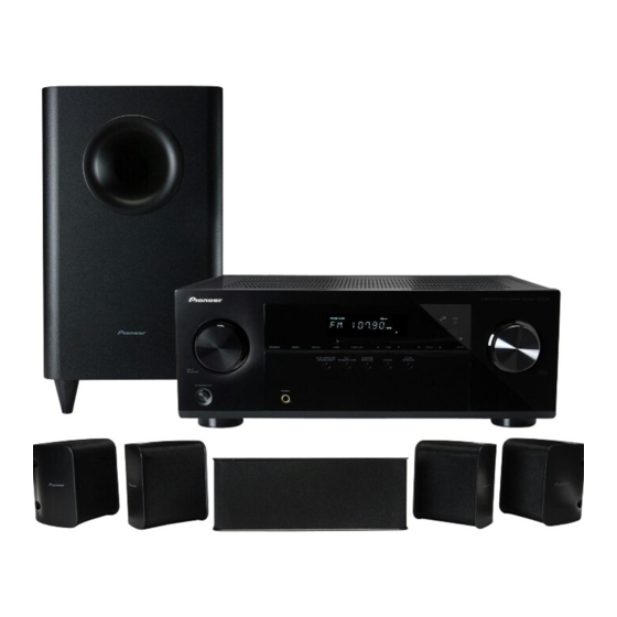
HOME CINEMA PACKAGE
HTP-071
AUDIO/VIDEO MULTI-CHANNEL RECEIVER
VSX-321-K-P
SUBWOOFER
S-22W-P
THIS MANUAL IS APPLICABLE TO THE FOLLOWING MODEL(S) AND TYPE(S).
Model
HTP-071
SYXE8
HTP-071
CXE
HTP-071
DLPWXE
HTP-071
AXE5
VSX-321-K-P
SYXE8
VSX-321-K-P
CXE
VSX-321-K-P
DLPWXE
VSX-321-K-P
AXE5
S-22W-P
—————
S-11-P
—————
HTP-071 is a Home Cinema Package and consists of VSX-321-K-P, S-22W-P and S-11-P.
PIONEER CORPORATION
PIONEER ELECTRONICS (USA) INC. P.O. Box 1760, Long Beach, CA 90801-1760, U.S.A.
PIONEER EUROPE NV Haven 1087, Keetberglaan 1, 9120 Melsele, Belgium
PIONEER ELECTRONICS ASIACENTRE PTE. LTD. 253 Alexandra Road, #04-01, Singapore 159936
PIONEER CORPORATION
Type
Power Requirement
AC 220 V to 230 V
AC 120 V
AC 220 V to 240 V
AC 220 V
AC 220 V to 230 V
AC 120 V
AC 220 V to 240 V
AC 220 V
—————
—————
1-1, Shin-ogura, Saiwai-ku, Kawasaki-shi, Kanagawa 212-0031, Japan
2011
Front
Surround
Center
HTP-071
SPEAKER SYSTEM
S-11-P
ORDER NO.
RRV4273
Remarks
K-IZV OCT.
2011 Printed in Japan
Advertisement
Table of Contents

Related Manuals for Pioneer VSX-321-K-P


Summary of Contents for Pioneer VSX-321-K-P
-
Page 1: Speaker System
————— S-11-P ————— ————— HTP-071 is a Home Cinema Package and consists of VSX-321-K-P, S-22W-P and S-11-P. PIONEER CORPORATION 1-1, Shin-ogura, Saiwai-ku, Kawasaki-shi, Kanagawa 212-0031, Japan PIONEER ELECTRONICS (USA) INC. P.O. Box 1760, Long Beach, CA 90801-1760, U.S.A. PIONEER EUROPE NV Haven 1087, Keetberglaan 1, 9120 Melsele, Belgium PIONEER ELECTRONICS ASIACENTRE PTE. -
Page 2: Safety Information
PIONEER Service Manual. A subscription to, or additional copies of, Also test with plug reversed Earth PIONEER Service Manual may be obtained at a nominal (Using AC adapter ground charge from PIONEER. plug as required) -
Page 3: Table Of Contents
8. EACH SETTING AND ADJUSTMENT ..........................49 8.1 UPDATING OF THE FIRMWARE ..........................49 9. EXPLODED VIEWS AND PARTS LIST..........................54 9.1 PACKING SECTION ..............................54 9.2 VSX-321-K-P SECTION ............................... 56 9.3 S-22W-P SECTION ..............................59 9.4 S-11-P SECTION................................60 10. SCHEMATIC DIAGRAM ..............................62 10.1 INPUT ASSY ................................ -
Page 4: Service Precautions
1. SERVICE PRECAUTIONS 1.1 NOTES ON SOLDERING • For environmental protection, lead-free solder is used on the printed circuit boards mounted in this unit. Be sure to use lead-free solder and a soldering iron that can meet specifications for use with lead-free solders for repairs accompanied by reworking of soldering. -
Page 5: Specifications
2. SPECIFICATIONS [VSX-321-K-P] Miscellaneous Power Requirements ..AC 220 V to 230 V, 50 Hz/60 Hz (SYXE8) Audio section AC 120 V, 60 Hz (CXE) (SYXE8) AC 220 V to 240 V, 50 Hz/60 Hz (DLPWXE) Rated power output Front, Center, Surround..100 W per channel (1 kHz, 6 Ω, 0.7 %) AC 220V, 50 Hz/60 Hz (AXE5) Power Consumption ...... - Page 6 Accessories Speaker cord (4 m) x 4 (8952S11005480-IL) Speaker cord (10 m) x 2 (8952S11005490-IL) Non-skid pads x 20 (8952S11005510-IL) Brackets for wall mounting x 4 Remote control (AXD7618) (8952S11005500-IL) (8300761800010-IL) Screw (M5) x 4 (8952S11005520-IL) Operating instructions (CD-ROM) (SYXE8 only) Dry cell batteries (6517000000440-IL) (AAA size IEC R03) x2...
-
Page 7: Basic Items For Service
Board to board extension jig cable GGD1772 Diagnosis (AMP Assy ↔ MAIN Assy) 3P extension jig cable GGD1773 Lubricants and Glues List Name Part No. Remarks Silicon grease GEM1057 Refer to "9.2 VSX-321-K-P SECTION". Silicon adhesive GYA1011 (KE40RTV-W) Refer to "9.2 VSX-321-K-P SECTION". HTP-071... -
Page 8: Pcb Locations
3.3 PCB LOCATIONS VSX-321-K-P DG ASSY D-MAIN ASSY CNT ASSY STBY ASSY MAIN ASSY G-T ASSY INPUT ASSY BR1 ASSY AMP ASSY G-L ASSY G-H ASSY HP ASSY FUNC ASSY FRONT ASSY NOTES: Parts marked by “NSP” are generally unavailable because they are not in our Master Spare Parts List. - Page 9 HTP-071...
-
Page 10: Block Diagram
4. BLOCK DIAGRAM 4.1 OVERALL CONNECTION DIAGRAM DG ASSY (7028071112010-IL) STBY ASSY (SYXE8: 7028071122040-IL) (CXE: 7028071122030-IL) (DLPWXE: 7028071122020-IL) CP603 (AXE5: 7028071122010-IL) 13P WAFER CP301 1/2- CP701 9P WAFER CP302 MAIN ASSY CP304 (SYXE8: 7028071121040-IL) (CXE: 7028071121030-IL) (DLPWXE: 7028071121020-IL) (AXE5: 7028071121010-IL) 8P WIRE 6P WIRE BD-TO... - Page 11 When ordering service parts, be sure to refer to "EXPLODED VIEWS and PARTS LIST" or "PCB PARTS LIST". The > mark found on some component parts indicates the importance of the safety factor of the part. Therefore, when replacing, be sure to use parts of identical designation. : The power supply is shown with the marked box.
-
Page 12: Overall Block Diagram
4.2 OVERALL BLOCK DIAGRAM FRONT ASSY INPUT ASSY HTP-071... - Page 13 ONT ASSY MAIN ASSY HP ASSY AMP ASSY PUT ASSY MAIN ASSY HTP-071...
-
Page 14: D-Main Block Diagram
4.3 D-MAIN BLOCK DIAGRAM D-MAIN ASSY SUB MICO I2C DATA EPF021A HDMI R/T Processor EP94A1K 74VHCU04 74LCX257MTCK A_R IN A_L IN TO INPUT PART I2C CONTROL BLOCK PCM9211 HTP-071... - Page 15 SN74LVC2GU04DCKR CEC-U UB MICOM MAIN MICOM EPF011C PF021A CONTROL LINE I2C DATA LOW PASS FILTER FR OUT FL OUT SR OUT 257MTCK SL OUT C OUT SW OUT SBR OUT SBL OUT HTP-071...
-
Page 16: Diagnosis
5. DIAGNOSIS 5.1 TROUBLESHOOTING [1] DSP TROUBLESHOOTING TROUBLESHOOTING FOR ALL DESTINATION Step 0: Preliminary confirmation Step 3: Regulator IC confirm the following items before checking IC609 (pin3) (to chassis) do screws of COAX jack securely tighten? Check the IC1 (pin 3) of Is the voltage of arround Tighten screws securely. - Page 17 Step 5: DIR Check that the S/PDIF signal is output. Check that changes by pulling out and inserting the digital input lines. 3: OPTICAL IC600 (pins 3,11) 11: COXIAL Check the path to OUTPUT Can observe the digital signal? pin of JACK601, JACK602. (0 V ↔...
- Page 18 Step 7: CODEC output (ANALOG) Step 6: DSP output (digital) to CODEC input Digital output of each CH when inputting the digital signal with audio. Analog output of each CH when inputting the digital signal with audio. IC601 (pin 7) IC603 (pin 1) DSP_BCK (BIT CLOCK) front R out...
- Page 19 [2] HDMI TROUBLESHOOTING HDMI Troubleshooting Cause for noncomplection of HDMI authentication between the source equipment and this unit. (the HDMI indicator is unlit or flasher) HDMI Simple Diagnosis Causes for no display or sound from the monitor Replace the HDMI cable. Replace the HDMI cable.
- Page 20 Step 2: Power supply CN601 (pin 14) CEC_ON Diagonose the MAIN Assy. Is the voltage 0 to 3.3 V? IC207 (pin 4) sub MICOM 3.3V Check the pin 5 of IC207. Is the voltage 3.3 V? CP104 (pins 1, 2) HDMI_10V Diagonose the MAIN Assy.
- Page 21 Step 3: Diagnosis Step 5: INPUT/OUTPUT Diagnosis Each data lines confirmation checks it after standby off/on. * when connected the equipment to CN601 (pin 10) JACK201 (pin 18) IN1 (CD/SAT): +5V_R317 (Not Insert) SUB_RESET Check the JACK201. If JACK201 Diagonose the MAIN Assy. Is the voltage 0 to 3.3 V? Is the voltage 5 V? is failure, replace JACK201.
- Page 22 Step 7: TMDS Step 6: SDA /SCL IC1002 (pins 30,31,33,34,36,37,39,40) TMDS OUTPUT IC201 (pin 7) SDA (HDMI_OUT) Check the IC1001 or IC1002. Are there signals If IC1001 or IC1002 is failure, (approx. 0.5 Vp-p) Check the JACK204 and IC201. replace IC1001 or IC1002. Does a signal output IN all lines? If JACK204 or IC201 is failure,...
-
Page 23: Protection Circuit
5.2 PROTECTION CIRCUIT HTP-071... -
Page 24: Ic Information
5.3 IC INFORMATION J046941000010-IL (EP94A1K)(D-MAIN ASSY: IC200) HDMI 1.3 4-In 1-Out Repeater with Audio Output • Pin Arrangement (Top View) X_IN EXT_SWING X_OUT AVSS VDDE RX23+ VDD_PLL RX23- PLL_XFC_A AVDD VSS_PLL RX13+ RX13- AVSS AVDD33 SPDIF RX03+ VSSE RX03- AVSS MCLK RXC3+ IIS_SCK... - Page 25 • Pin Function HDMI Input Ports Name In/Out Description RXC0- Differential Clock Input Pair for HDMI Input Port 0 RXC0+ Differential Clock Input Pair for HDMI Input Port 0 RX00- Differential Data Input Pair0 for HDMI Input Port 0 RX00+ Differential Data Input Pair0 for HDMI Input Port 0 RX10- Differential Data Input Pair1 for HDMI Input Port 0...
- Page 26 • Pin Function Audio Outputs Name In/Out Description MCLK System Clock output for audio DAC (128/256/384/512 * FSampling_Clock. Connecting a pull-up (logic 1) or pull-down (logic 0) resistor at this pin defines bit 4 of the slave IIC Address IIS_SCK IIS SCK output for IIS audio port.
- Page 27 8952VS3210020-IL (EPF021A) (D-MAIN ASSY: IC201) Generic Microcontroller Unit • Pin Arrangement (Top View) P2[1] P0[5] P2[2] P0[4] P2[3] P0[3] P2[4] P0[2] P2[5] P0[1] P2[6] P0[0] P2[7] P5[7] P5[6] TIM[0] P5[5] TIM[1] P5[4] P1[0] P1[1] P5[3] P1[2] P5[2] P1[3] P5[1] P7[0] P5[0] P7[4](CIR) P7[1]...
- Page 28 • Pin Function Name In/Out Buffer Type Description OP_MODE IXDXXP Chip operation mode. 0: Normal mode 1: ICP (In Circuit Flash Programming) mode RSTb BDUX8P External Reset (active low) with on-chip pull-up. When this pin is asserted low, the chip is totally reset. X_IN XTL24P 24 MHz crystal input...
- Page 29 8952VS3210030-IL (EPF011C) (D-MAIN ASSY: IC203) Generic MCU with 64K Embedded Flash • Pin Arrangement (Top View) P7[0](RXD) P1[1] P7[1](TXD) P8[7](PWM) P4[1] P2[1] P3[0] P3[1] P3[4] X_OUT P3[5] X_IN RSTb OP_MODE P9[0] P0[2] P7[4](CIR) P0[1] P5[0] P0[0] • Block Diagram Port 0 256B Direct Port 1 Data RAM...
- Page 30 • Pin Function Name In/Out Buffer Type Description OP_MODE IXDXXP Chip operation mode. 0: Normal mode 1: ICP (In Circuit Flash Programming) mode NOTE: The input crystal rate will be 24 MHz if this ICP mode is used. RSTb BDUX8P External Reset (active low) with on-chip pull-up.
- Page 31 PCM1681 (D-MAIN ASSY: IC601) 24-Bit, 192-kHz Sampling, Enhanced Multilevel Delta-Sigma, Eight-Channel Audio Digital-to-Analog Converter • Pin Arrangement (Top View) ZR1/ZR1/FMT0 MS/ADR/FMT1 MC/SCL/DEMP MD/SDA/MUTE AGND2 DATA1 LRCK DGND DATA2 AGND1 DATA3 DATA4 MSEL • Block Diagram Output Amp and Low-Pass Filter LRCK Output Amp and Low-Pass Filter...
- Page 32 • Pin Function Name In/Out Description ZR1/ZR1/FMT0 Zero-flag output 1 for SPI, zero-flag output 1 for I2C, format control input 0 for H/W(1) Select input for SPI, address input for I2C, format control input 1 for H/W (1) (2) MS/ADR/FMT1 MC/SCL/DEMP Shift clock input for SPI, serial clock input for I2C, de-emphasis control for H/W (1) (2) MD/SDA/MUTE...
- Page 33 J046921100710-IL (PCM9211) (D-MAIN ASSY: IC602) 216-kHz Digital Audio Interface Transceiver (DIX) with Stereo ADC and Routing • Pin Arrangement (Top View) ERROR/INT0 VDDRX NPCM/INT1 RXIN1 MPIO_A0 MPIO_A1 RXIN2 MPIO_A2 RXIN3 MPIO_A3 RXIN4/ASCKIO PCM9211 MPIO_C0 RXIN5/ABCKIO MPIO_C1 RXIN6/ALRCKIO MPIO_C2 RXIN7/ADIN0 MPIO_C3 MODE MPIO_B0 MS/ADR1...
- Page 34 • Block Diagram FILT AUXIN 0 AUTO RXIN7 RXIN 0 RXIN0 SCKO DOUT RXIN 1 RXIN1 MAIN OUTPUT AUXIN0 LRCK RXIN 2 RXIN2 SCKO/ BCK/LRCK PORT RXIN 3 RXIN3 AUXIN1 DOUT Lock :DIR AUXIN2 RXIN 4/ASCKI 0 RXIN4 Unlock:ADC RXIN 5/ABCKI 0 RXIN5 Clock/ Data Recovery...
- Page 35 • Pin Function Name In/Out Description ERROR/INT0 DIR Error detection output / Interrupt0 output DIR Non-PCM detection output / Interrupt1 output NPCM/INT1 MPIO_A0 Multipurpose I/O, Group A(1) MPIO_A1 Multipurpose I/O, Group A(1) MPIO_A2 Multipurpose I/O, Group A(1) MPIO_A3 Multipurpose I/O, Group A(1) MPIO_C0 Multipurpose I/O, Group C(1) MPIO_C1...
-
Page 36: Service Mode
6. SERVICE MODE 6.1 SERVICE MODE [1] Display mode for numbers of protection detections [Purpose] The numbers of detections for various protection processes are displayed. [How to enter/exit] During Standby mode, simultaneously press and hold the [PRESET –] and [STANDBY/ON] keys for 2 seconds to enter this mode. - Page 37 [2] Reset mode for numbers of protection detections [Purpose] For clearing all the counts of protection detections. (This mode resets the counts of protection detections.) [How to enter/exit] During Standby mode, simultaneously press and hold the [ALC/STANDARD SURR] and [STANDBY/ON] keys for 10 seconds to enter this mode.
- Page 38 TEMP (AMP overheat) error detection For detection of a TEMP error, the unit monitor THER_DET (PROTECT2) signal. If a TEMP error is detected, the processes shown below will be performed. The processes shown below are rough operational specifications and are not the actual commands from the mounted components.
-
Page 39: Disassembly
7. DISASSEMBLY 7.1 VSX-321-K-P Note: (1) Even if the unit shown in the photos and illustrations in this manual may differ from your product, the procedures described here are common. (2) For performing the diagnosis shown below, the following jigs for service is required: •... - Page 40 2. Notes on Disassembly and Reassembly Confirmation of Connection After completion of reassembly, before plugging the power cord into an outlet, make sure that the 4P wires from CN5 of the MAIN Assy are connected to CP104 of the D-MAIN Assy. If the unit is turned ON without these wires connected, the CODEC IC (IC602) on the D-MAIN Assy may be damaged.
- Page 41 3. Disassembly [1] Front Panel Section Remove the cabinet by removing the 10 screws. (1) Remove the five screws. (BBZ30P080FTB) • Bottom view (2) Remove the two screws. (1500001206010-IL) (3) Unhook the two hooks. (4) Arrange the front panel section as shown in the photo below.
- Page 42 [2] Heatsink Section Caution: Heatsink section in work becomes hot, and be careful with it. Remove the cabinet by removing the 10 screws. (1) Remove the three screws. (BBZ30P080FTC) • Bottom view (2) Remove the seven screws. G-L Assy (BBZ30P080FTC) G-H Assy (3) Release the five binders.
- Page 43 (6) Disconnect the one connector. MAIN Assy (CP404) CP404 AMP Assy (7) Connect the extension jig cable. Extension jig cable (AMP CN203 ↔ MAIN CP404) (GGD1773) AMP Assy (8) Rotate the heatsink section in the direction of the arrow. Heatsink [3] D-MAIN Assy Remove the cabinet by removing the 10 screws.
- Page 44 (3) Cut the binder. BR1 Assy (4) Disconnect the two B to B connectors. (CN600, CN601) (5) Remove the D-MAIN and DG Assemblies. CN209 CN600 CNT Assy D-MAIN Assy DG Assy CN1000 CN601 (6) Disconnect the one B to B connector and remove the CNT Assy.
- Page 45 [4] MAIN Assy Remove the cabinet by removing the 10 screws. [4-1] Chassis back Chassis back (1) Remove the nine screws. • Rear view (BBT30P100FTB) (2) Remove the two screws. (SYXE8, DLPWXE only)(CBZ30P080FTB) (3) Remove the chassis back. [4-2] MAIN Assy (1) Remove the three screws.
- Page 46 [4-3] Regulator ICs and Recifier diode (1) Remove the support. MAIN Assy (2) Tighten then loosen the screw in each of the Screwdriver four holes for temporary joining that are located on the rear side of the main chassis. (This is for shaving the thread grooves to facilitate attachment in the next step.) Main chassis Support...
-
Page 47: S-22W-P
[4-4] Diagnosis (1) Remove the one screw and remove the earth lead jumper. (BBZ30P080FTC) (2) Reassemble the earth lead jumper. Earth lead jumper Earth lead jumper G-H Assy G-H Assy (3) Insert any insulation sheet between AMP Assy and MAIN Assy. Insulation sheet AMP Assy MAIN Assy... -
Page 48: S-11-P
7.3 S-11-P Removing the FRONT / SURROUND SPEAKER 1. Remove the four screws. 2. Press on the grille bottom with both thumbs and slide it in frontward direction of the speaker while pressing with sufficient force. (Fig.1) 3. Press on the grille bottom with both thumbs and slide it in frontward direction of the speaker while pressing with sufficient force. -
Page 49: Each Setting And Adjustment
8. EACH SETTING AND ADJUSTMENT 8.1 UPDATING OF THE FIRMWARE [Purpose] Refer to this section when updating the firmware of each microcomputer is required by the service information, etc. [Necessary Tools and Connections] 1 MAIN microcomputer • PC with a serial port •... - Page 50 Connect as shown in the figure below. Insert the FFC with its contact surface facing the " mark. USB cable (HDMI/CEC microcomputer) 10P to 10P FFC UPDATE jig GGF1646 Rear side USB cable A type <-> B type Microcomputers update [Procedures] for MAIN microcomputer [ if the following messages are displayed ]...
- Page 51 5. Set speed update and update the MCU. 1 Set speed of update. 1 Set speed of update. Set Baud rate to 38400. Press the OK button. 2 Update the MCU. E.P.R=>Erase+Program+Read 7. Unplug the AC cord. Disconnect the FFC cable. 2 Update the MCU Press the E.P.R …...
- Page 52 11. Select the update file. Press the "OpenFile" button. End the application EPFlash. If the following messages are displayed, shut the update program down, and start the update again from step 8. Select "VSX-321_LPP_********.hex" file to update MCU. 12. Press the "START" button to update the firmware. 14.
- Page 53 17. Select the update file. Press the "FILE" button. 19. Press the button. 20. Press the button to update the firmware. Select "CECCore_ADDSEL(BB)_V***.hex" file to update MCU. Rate of the progression is appeared. When the update file is selecting, the check box is automatically on.
-
Page 54: Exploded Views And Parts List
For the applying amount of lubricants or glue, follow the instructions in this manual. (In the case of no amount instructions, apply as you think it appropriate.) 9.1 PACKING SECTION S-11-P VSX-321-K-P Poly bag Style Poly bag Packing Style Tape (Clear) - Page 55 (1) PACKING SECTION PARTS LIST Mark No. Description Part No. Mark No. Description Part No. 16 Operating Instructions See Contrast table (2) 1 Power Cord See Contrast table (2) 17 Operating Instructions See Contrast table (2) 2 AM Loop Antenna E601019000010-IL 18 Operating Instructions See Contrast table (2)
-
Page 56: Vsx-321-K-P Section
9.2 VSX-321-K-P SECTION DLPWXE only Cushion EVA HTP-071... - Page 57 for CXE, AXE5 for SYXE8, DLPWXE ×23 Silicon adhesive (GYA1011) Heatsink Silicon grease (GEM1057) HTP-071...
- Page 58 See Contrast table (2) 60 Screw 1500001206010-IL 30 Front Panel See Contrast table (2) 61 Screw 1500001456010-IL (2) CONTRAST TABLE VSX-321-K-P/SYXE8, CXE, DLPWXE and AXE5 are constructed the same except for the following: VSX-321-K-P VSX-321-K-P VSX-321-K-P VSX-321-K-P Mark Symbol and Description /SYXE8...
-
Page 59: S-22W-P Section
9.3 S-22W-P SECTION S-22W-P SECTION PARTS LIST Mark No. Description Part No. 1 Unit Assy 8952S22W00009-IL 2 Network Assy 8952S22W00011-IL 3 Speaker Terminal 8952S22W00004-IL 4 Foot Mold 8952S22W00007-IL 5 Foot Cushoin 8952S22W00200-IL 6 Cashmere 8952S22W00210-IL 7 Screw (Bind Head) 8952SHM700039-IL 8 Screw (Bind Head) 8952S21W05381-IL HTP-071... -
Page 60: S-11-P Section
9.4 S-11-P SECTION Front L, R, Surround L, R speaker Center speaker HTP-071... - Page 61 S-11-P SECTION PARTS LIST Mark No. Description Part No. Front L, R, Surround L, R speaker 1 Unit Speaker (Surround) 8952S11005250-IL 2 Speaker Wire 8952S11005140-IL 3 Speaker Terminal 8952S11005100-IL 4 Frame Net Assy 8952S11005350-IL 5 Case Rear 8952S11005380-IL 6 Felt 8952S11005411-IL 7 Cassimere 8952S11005430-IL...
-
Page 62: Schematic Diagram
10. SCHEMATIC DIAGRAM 10.1 INPUT ASSY R598 (SBL) R516 R509 C443 (SBL) R438 R439 10/50 R437 R445 R446 Q408 - INC2001AC1 C424 47N(EB)-100V C411 47N-K Q411 - INC2001AC1 R451 R452 C453 R454 R455 R456 C423 10/50 22N(EB)-100V LUG500 1P200mm C457 C441 R462 10/50... - Page 63 INPUT ASSY (7028071111010-IL) D402 KDS4148U (FL) R403 C401 D401 R404 KDS4148U 10/50 R409 R410 Q402 D404 INC2001AC1 KDS4148U (SL) CN400 R414 D403 C406 R415 C407 2.0MM-12P KDS4148U 10/50 R420 R421 C409 Q405 D406 INC2001AC1 KDS4148U C419 R426 C420 R427 10/50 C426 CP201 R428...
-
Page 64: Amp Assy
10.2 AMP ASSY AMP ASSY (7028071141010-IL) 2SD2390Y Q205SR C207SR R218SR R205SR R226SR 470K 47(1/4) 47/50(6.3*11) R224SR Q207SR C203SR C204SR KTC3200BL 220P-500V 33P-500V R214SR Q202SR C201SR R201SR R206SR KSA992F Q201SR 10/50 Q204SR KSA992F R204SR 2SC3964 R208SR R219SR 47(1/4) Q206SR Q203SR 2SB1560Y KTC3200BL (FL) CP201... - Page 65 2SD2390Y Q205FR C207FR R218FR R205FR 470K R226FR 47(1/4) 47/50(6.3*11) R224FR Q207FR C203FR C204FR KTC3200BL 220P-500V 33P-500V R214FR Q202FR R201FR C201FR R206FR KSA992F Q201FR 10/50 KSA992F Q204FR R204FR 2SC3964 R219FR R208FR 47(1/4) Q206FR Q203FR 2SB1560Y KTC3200BL CP202 C214 10/50 C217 10/100(6.3*11) C212 2SD2390Y C218...
-
Page 66: Main Assy (1/2)
10.3 MAIN ASSY (1/2) SPEAKER TERMINAL CN721 CP17 20010WS-04 C125Z1-27 1N-K 1N-K 1N-K 1N-K 1N-K 1N-K (HP) RLY1 (HP) RT1P237C RT1P RT1N237C RT1N 1SS133T 2K2(1) 2K2(1) 2K2(1) 10/50 GBJ1006 100N(EB)-100V TO CHASSIS CP203 100N(R)-250V CP202 100N(R)-250V 100N(R)-250V C112 10N-K GND2 0R1(5) KBPC604-6A C116... - Page 67 CP401 MAIN ASSY (MAIN BLOCK) (SYXE8: 7028071121040-IL) (CXE: 7028071121030-IL) (DLPWXE: 7028071121020-IL) (AXE5: 7028071121010-IL) Z1-27 R632 R625 (SW) (SW) JACK4 R626 R629 C627 R630 R627 R43 - Q602 C612 Q603 JACK3 100N-K BH76330FVM 100N-K 470/6.3(6.3*11) 100N-K 47/16 47N-Z /RST /SEN SCLK SDIO 10N-K VCC_5V...
-
Page 68: Main Assy (2/2)
10.4 MAIN ASSY (2/2) R268 CP1000 CP201 C125Z1-29 R269 C208 100N-K C209 330P-J C242 10N-K C214 R312 R317 R300 IC203 R299 M3030RFGPFP R298 R275 R223 R225 Q201 ISA1530AC1 C216 C243 D201 100N-K KDS4148U C217 100/10 C241 C220 10N-K Q202 RT1N237C R249 R250 R256... - Page 69 MAIN ASSY (CPU BLOCK) FPC201 1.0-11S-10PW (SYXE8: 7028071121040-IL) (CXE: 7028071121030-IL) (DLPWXE: 7028071121020-IL) (AXE5: 7028071121010-IL) R268 R269 D311 R325 R207 M150(1) 1SS133T R208 R209 CN704 R221 R222 1.25-2-27P R315 R316 R313 IC203 M3030RFGPFP R338 100 R339 100 R340 100 R323 R324 C215 10N-K C246...
-
Page 70: D-Main Assy (1/3)
10.5 D-MAIN ASSY (1/3) Q208 R290 2.2/50 R318 R289 R288 100N-K C208 C201 100N-K 100N-K C202 100N-K C203 IC200 100N-K C204 EP94A1K 100N-K C205 100N-K C206 R243 Q205 R317 100N-K C207 R213 100N-K C270 R222 C213 R228 100N-K C215 C221 C217 100N-K 100N-K... - Page 71 D-MAIN ASSY (HDMI BLOCK) (7028071161010-IL) 18M432MHZ C225 R246 XTAL201 2.2/50-Z8154 1N-K R248 C226 C240 1/50-Z8155 CB207 CB208 C239 10/16-Z8154 R329 R267 R330 R331 CB218 R258 R259 CB217 IC200 EP94A1K R285 C250 CB213 R284 R283 CB214 C242 R282 100N-K R281 C245 R280 100N-K R279...
-
Page 72: D-Main Assy (2/3)
10.6 D-MAIN ASSY (2/3) 470P-J C604FR R601FR R603FR C602FR R600FR 10/16-Z8154 AZ4580M C601FR 4N7-K IC603 470P-J C604FL C608 R603FL C602FL (FL) 1N-K R600FL R601FL 10/16-Z8154 (FL) C601FL 4N7-K C607 1N-K 470P-J C604SR IC601 R601SR R603SR C602SR PCM1681 R600SR 10/16-Z8154 C624 10/16-Z8154 C625 AZ4580M... - Page 73 D-MAIN ASSY (CODEC BLOCK) (7028071161010-IL) R653 R656 300K C659 47P-J IC600 74VHCU04 C661 47P-J R657 R651 R612 L141 LBC2012T-4.7UH C641 C639 C640 68N-K 10/16-Z8154 10/16-Z8154 C645 C646 100N-K 100N-K C609FL 10/16-Z8154 R270 R271 C609FR 10/16-Z8154 R314 R272 100K C634 C636 R273 R313 R646...
-
Page 74: D-Main Assy (3/3)
10.7 D-MAIN ASSY (3/3) L151 D160 L150 R738 R721 R722 R723 R724 R725 R726 R727 R729 R704 R730 IC101 R731 74LCX257MTCX R732 R702 R733 R703 C462 220N-K R705 R714 R707 0 R735 R701 R708 0 R711 R706 R709 R736 R741 R742 HTP-071... - Page 75 D-MAIN ASSY (DSP BLOCK) (7028071161010-IL) C530 470/6.3-Z8158 C532 C526 220N-K C527 C533 1N-K C528 33P-J C534 94 93 220N-K C529 100N-K R787 R788 C524 10P-D R789 R790 R791 R792 R793 R794 IC102 R795 C531 220N-K IC103 R796 IS42S16400F-6TL R797 L158 R818 R798 R799...
-
Page 76: Br1, Hp, Func And Front Assys
10.8 BR1, HP, FUNC and FRONT ASSYS BR1 ASSY (7028071133010-IL) CN600 CN209 C125Z1-23 (SBL) C250SBL 10P-D C250SBR 10P-D (SW) CP400 (SL) (FL) : Audio Signal Route (Front L ch) (FL) (SL) : Audio Signal Route (Surround L ch) : Audio Signal Route (Center ch) (SW) : Audio Signal Route (SubWoofer ch) (SBL) - Page 77 FRONT ASSY (7028071131010-IL) C727 10N-K C766 C728 10/50 R737 IC701 SC16315 MTZ7.5B CN701 C746 270MM/9P R779 2R2(1/4) FLCT R780 GNDU 2R2(1/4) CP701 CPU+3.3V CPU_ST_VCC C767 C753 C756 STBY_RLY 10N-K C730 HDMI+12V 1/50 C760 C762 Q702 2SA933S R778 Q703 RT1N144C STBY_KEY INPUT_UP GNDU INPUT_DN...
-
Page 78: Dg Assy
10.9 DG ASSY DG ASSY (7028071112010-IL) R615 R616 JACK601 L601 LBC2012T-4.7UH CN603 R612 R613 R614 HTP-071... -
Page 79: Cnt, G-T, G-L And G-H Assys
10.10 CNT, G-T, G-L and G-H ASSYS CNT ASSY (7028071151010-IL) BD1001 BD121T BD1002 BD121T BD1003 BD121T BD1004 BD121T BD1005 BD121T BD1006 BD121T BD1007 BD121T BD1008 BD121T BD1009 BD121T G-T ASSY (7028071123010-IL) G-L ASSY (7028071125010-IL) G-H ASSY (7028071124010-IL) CLAMP904 CLAMP903 CLAMP_WIRE CLAMP_WIRE CLAMP906 CLAMP907... -
Page 80: Stby Assy
10.11 STBY ASSY STBY ASSY (SYXE8: 7028071122040-IL) (CXE: 7028071122030-IL) (DLPWXE: 7028071122020-IL) (AXE5: 7028071122010-IL) • NOTE FOR FUSE REPLACEMENT CAUTION - FOR CONTINUED PROTECTION AGAINST RISK OF FIRE, REPLACE WITH SAME TYPE AND RATINGS OF FUSE. ZD303 MTZJ7.5B R326 D301 R333 CP302 D302 KDS4148U... -
Page 81: S-11-P
10.12 S-11-P Speaker Wire (8952S11005140-IL) Poly S/W-110 INPUT Speaker White P.SW: P.SW has extreme positive resistance-temperature characteristics. If an abnormal current flows to P.SW due to an excessive input or unusual signal, P.SW heats up and the resistance rapidly increases. With this function, the speakers are protected from excessive input or unusual signal. -
Page 82: Pcb Connection Diagram
11. PCB CONNECTION DIAGRAM 11.1 INPUT ASSY SIDE A INPUT ASSY Q411 Q416 Q408 Q414 Q417 Q412 Q409 Q415 IC400 Q402 Q405 Q413 Q407 Q406 Q410 IC403 IC402 Q427 Q426 Q421 Q420 Q419 CP400 CN210 HTP-071... - Page 83 SIDE B NOTE FOR PCB DIAGRAMS : 2. View point of PCB diagrams. Connector Capacitor 1. The parts mounted on this PCB include all necessary parts for several destinations. SIDE A For further information for respective desti- nations, be sure to check with the sche- matic diagram.
-
Page 84: Amp Assy
11.2 AMP ASSY SIDE A CN400 AMP ASSY CP202 CP201 CP203 Q208 Q202FR Q201FR Q202SR Q201SR Q202C Q201C Q207FR Q203FR Q207SR Q203SR Q207C Q203C Q205FR Q204FR Q206FR Q205SR Q204SR Q206SR Q205C Q204C Q206C SIDE B AMP ASSY CP203 CP202 CP201 HTP-071... - Page 85 SIDE A CN400 CP201 CP203 Q202SW Q201SW Q202SL Q201SL Q202FL Q201FL Q207SW Q203SW Q207SL Q203SL Q207FL Q203FL Q206C Q205SW Q204SW Q206SW Q205SL Q204SL Q206SL Q205FL Q204FL Q206FL SIDE B CP203 CP201 HTP-071...
-
Page 86: Main Assy
11.3 MAIN ASSY SIDE A MAIN ASSY MAIN TRANS. MAIN TRANS. HTP-071... - Page 87 SIDE A CP401 CP17 MAIN TRANS. MAIN TRANS. HTP-071...
- Page 88 SIDE B MAIN ASSY CP17 Q215 Q217 Q603 Q602 Q212 Q216 IC203 Q202 Q201 Q210 Q209 Q211 IC204 Q206 Q203 HTP-071...
- Page 89 SIDE B HTP-071...
-
Page 90: D-Main Assy
11.4 D-MAIN ASSY SIDE A D-MAIN ASSY HTP-071... - Page 91 SIDE A CP603 CN603 IC600 IC609 IC205 IC101 IC602 IC206 IC601 IC200 IC102 IC100 IC608 IC203 IC201 IC202 IC207 IC103 IC607 Q208 Q204 CN1000 CN601 HTP-071...
- Page 92 SIDE B D-MAIN ASSY CN603 IC606 IC605 IC604 IC603 IC104 CN601 HTP-071...
- Page 93 SIDE B HTP-071...
-
Page 94: Br1, Hp, Func And Front Assys
11.5 BR1, HP, FUNC and FRONT ASSYS SIDE A HP ASSY BR1 ASSY Q702 CP400 CN210 FUNC ASSY CN702 CP702 SIDE B CP702 CN702 Q705 FUNC ASSY CN210 Q703 Q707 Q701 BR1 ASSY HP ASSY E F G H HTP-071... - Page 95 SIDE A FRONT ASSY CN704B RMC701 CN704 SIDE B CN704 IC701 Q706 Q708 Q704 Q709 FRONT ASSY HTP-071...
-
Page 96: Dg Assy
11.6 DG ASSY SIDE A SIDE A DG ASSY CP603 CN603 SIDE B SIDE B DG ASSY CP603 HTP-071... -
Page 97: Cnt Assy
11.7 CNT ASSY SIDE A SIDE A CNT ASSY CP1000 CN1000 CP201 CN601 SIDE B SIDE B CP1000 CN1000 CNT ASSY HTP-071... -
Page 98: G-T, G-L And G-H Assys
11.8 G-T, G-L and G-H ASSYS SIDE A SIDE A G-T ASSY G-L ASSY G-H ASSY SIDE B SIDE B G-H ASSY G-T ASSY G-L ASSY HTP-071... -
Page 99: Stby Assy
11.9 STBY ASSY SIDE A SIDE A STBY ASSY SIDE B SIDE B STBY ASSY Q303 Q302 IC301 Q301 HTP-071... -
Page 100: Pcb Parts List
12. PCB PARTS LIST NOTES: Parts marked by “NSP” are generally unavailable because they are not in our Master Spare Parts List. The > mark found on some component parts indicates the importance of the safety factor of the part. Therefore, when replacing, be sure to use parts of identical designation. - Page 101 N751503151160-IL CN9302 CN, WAFER 7.92 mm L108353280290-IL L108011430210-IL L108011430210-IL L108011430210-IL 304 BRACKET 4010210196100-IL 4010210196000-IL 4010210196000-IL 4010210196000-IL PARTS LIST for VSX-321-K-P/SYXE8 Mark No. Description Part No. Mark No. Description Part No. C 204 D00033006D051-IL INPUT ASSY C 209,210 D00410107D051-IL SEMICONDUCTORS IC 400...
- Page 102 Mark No. Description Part No. Mark No. Description Part No. CN 9001 CONNECTOR L108353280360-IL CN 9002 CN.WAFER 3.96MM L104353130360-IL D 251 K005041480030-IL CN 9003,9004 CONNECTOR(3P) L102526700300-IL D 266-276 K067020500010-IL CN 9005 CN.WAFER 2.0MM L101200100410-IL CN 9017 CN.WAFER L109012512710-IL MISCELLANEOUS L 141,153 COIL,INDUCTOR D3104R7010200-IL CN 9201 CN,WAFER L109012512910-IL...
- Page 103 Mark No. Description Part No. Mark No. Description Part No. CN 704 CN.FPC 1.25MM L131125022720-IL RESISTORS R 326 C060033065050-IL RESISTORS R 779,780 C0602R2063050-IL CAPACITORS C 301 D040222083010-IL C 304 D00847208H010-IL DG ASSY SEMICONDUCTORS D 416 K005041480030-IL MISCELLANEOUS JA 601 OPTICAL RECEIVER E100116500040-IL JA 602 TER,RCA 1PIN...
Need help?
Do you have a question about the VSX-321-K-P and is the answer not in the manual?
Questions and answers