
Related Manuals for National Instruments PCI-DIO-96


Summary of Contents for National Instruments PCI-DIO-96
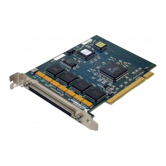
- Page 1 PCI-DIO-96/PXI-6508/PCI-6503 User Manual 96-Bit and 24-Bit Parallel Digital I/O Interface for PCI, PXI, and CompactPCI PCI-DIO-96/PXI-6508/PCI-6503 User Manual March 2009 374938B-01...
- Page 2 Thailand 662 278 6777, Turkey 90 212 279 3031, United Kingdom 44 (0) 1635 523545 For further support information, refer to the Technical Support and Professional Services appendix. To comment on National Instruments documentation, refer to the National Instruments Web site at and enter ni.com/info the info code feedback ©...
-
Page 3: Important Information
Instruments Corporation. National Instruments respects the intellectual property of others, and we ask our users to do the same. NI software is protected by copyright and other intellectual property laws. Where NI software may be used to reproduce software or other materials belonging to others, you may use NI software only to reproduce materials that you may reproduce in accordance with the terms of any applicable license or other legal restriction. -
Page 4: Table Of Contents
Chapter 2 Installation and Configuration Software Installation ......................2-1 Installing NI-DAQ...................2-1 Installing Other Software ................2-1 Hardware Installation.....................2-1 Installing the PCI-DIO-96 or PCI-6503 ............2-1 Installing the PXI-6508 ...................2-2 Board Configuration ......................2-2 Chapter 3 Signal Connections I/O Connector (PCI-DIO-96, PXI-6508) ...............3-1 I/O Connector Pin Assignments ..............3-1 Cable Assembly Connectors................3-3... - Page 5 Mode 2 Bidirectional Timing................4-7 Appendix A Specifications Appendix B Register-Level Programming 82C53 Programmable Interval Timer (PCI-DIO-96, PXI-6508 Only) ......B-2 Interrupt Control Circuitry ................B-2 Register Map and Description ..................B-4 Introduction ..................... B-4 Register Map ....................B-5 Register Descriptions ..................B-6 Register Description Format.............
- Page 6 Appendix C Technical Support and Professional Services Glossary Index Figures Figure 3-1. PCI-DIO-96 and PXI-6508 Connector Pin Assignments......3-2 Figure 3-2. Cable-Assembly Connector Pinout for the R1005050 Ribbon Cable (PCI-DIO-96 and PXI-6508)..........3-3 Figure 3-3. PCI-6503 I/O Connector Pin Assignments ...........3-6 Figure 3-4.
- Page 7 Table 3-2. PCI-6503 Signal Descriptions ............. 3-7 Table 3-3. Port C Signal Assignments ..............3-8 Table 4-1. The 82C55A Chips Used in the PCI-DIO-96, PXI-6508, and PCI-6503 ..................4-3 Table 4-2. Signal Names Used in Timing Diagrams ..........4-4 Table B-1.
-
Page 8: About This Manual
PCI-DIO-96 and PCI-6503 are members of the National Instruments PCI Series of expansion boards for PCI bus computers. The PXI-6508 is a member of the National Instruments PXI family of expansion boards for PXI and CompactPCI chassis. These boards are designed for... -
Page 9: Related Documentation
(PPI) chips on the PCI-DIO-96 or PXI-6508. The PCI-6503 contains only one PPI, PPI A. Your DIO board Your DIO board refers to either the PCI-DIO-96, PXI-6508, or PCI-6503 board. Related Documentation The following National Instruments document contains information that you may find helpful as you read this manual. -
Page 10: Introduction
I/O interface for PCI bus computers. Four 82C55A programmable peripheral interface (PPI) chips control the 96 bits of TTL-compatible digital I/O on the PCI-DIO-96 or PXI-6508. On the PCI-6503, one 82C55A PPI controls the 24 bits of TTL-compatible digital I/O. -
Page 11: Using Pxi With Compactpci
Your PXI-6508 device works in any standard CompactPCI chassis adhering to the PICMG 2.0 R2.1 CompactPCI core specification. What You Need to Get Started To set up and use your PCI-DIO-96/PXI-6508/PCI-6503 board, you will need the following: ❑ PCI-DIO-96, PXI-6508, or PCI-6503 board ❑... -
Page 12: Optional Equipment
Chapter 1 Introduction Optional Equipment National Instruments offers a variety of products to use with your DIO board, including cables, connector blocks, and other accessories, as follows: • Cables and cable assemblies • Connector blocks, 50-pin screw terminals • SCXI modules and accessories for isolating, amplifying, exciting, and multiplexing signals for relays and analog output. -
Page 13: Unpacking
Chapter 1 Introduction The mating connector for the PCI-6503 is a 50-position, polarized ribbon socket connector with strain relief. National Instruments uses a polarized (keyed) connector to prevent inadvertent upside-down connections. Recommended manufacturer part numbers for this mating connector are as follows: •... -
Page 14: Installation And Configuration
Installing the PCI-DIO-96 or PCI-6503 To install a PCI-DIO-96 or PCI-6503 in any available 5 V PCI expansion slot in your computer, complete the following steps: Turn off and unplug your computer. -
Page 15: Installing The Pxi-6508
Touch the metal part inside your computer to discharge any static electricity that might be on your clothes or body. Insert the PCI-DIO-96 or PCI-6503 in a 5 V PCI slot. It may be a tight fit, but do not force the device into place. -
Page 16: Signal Connections
Instruments signal conditioning devices, go to ni.com/signalconditioning I/O Connector (PCI-DIO-96, PXI-6508) The I/O connector for the PCI-DIO-96 and PXI-6508 has 100 pins that you can connect to 50-pin accessories with the R1005050 cable. I/O Connector Pin Assignments Figure 3-1 shows the pin assignments for the PCI-DIO-96 and PXI-6508 digital I/O connector. -
Page 17: Figure 3-1. Pci-Dio-96 And Pxi-6508 Connector Pin Assignments
BPC1 DPC1 APC1 CPC1 BPC2 DPC2 APC2 CPC2 BPC3 DPC3 CPC3 APC3 DPC4 BPC4 CPC4 APC4 DPC5 BPC5 CPC5 APC5 DPC6 BPC6 CPC6 APC6 DPC7 BPC7 CPC7 APC7 Figure 3-1. PCI-DIO-96 and PXI-6508 Connector Pin Assignments PCI-DIO-96/PXI-6508/PCI-6503 User Manual ni.com... -
Page 18: Cable Assembly Connectors
Both cables are joined to a single connector on one end and to individual connectors on the free ends. The 100-pin connector that joins the two cables plugs into the I/O connector of the PCI-DIO-96 and PXI-6508. The other two connectors are 50-pin connectors, one of which is connected to pins 1 through 50 and the other connected to pins 51 through 100 of the PCI-DIO-96 and PXI-6508 connector. -
Page 19: I/O Connector Signal Descriptions
Chapter 3 Signal Connections I/O Connector Signal Descriptions Table 3-1 lists the signal descriptions for the PCI-DIO-96 and PXI-6508 I/O connector pins. Table 3-1. Signal Descriptions for PCI-DIO-96 and PXI-6508 I/O Connectors Alternate † Signal Name Port ID Description 1, 3, 5, 7, 9, 11, 13, 15 APC<7..0>... - Page 20 Chapter 3 Signal Connections Table 3-1. Signal Descriptions for PCI-DIO-96 and PXI-6508 I/O Connectors (Continued) Alternate † Signal Name Port ID Description 67, 69, 71, 73, 75, 77, CPB<7..0> Bidirectional data lines for port B 79, 81 of PPI C—CPB7 is the MSB, CPB0 is the LSB.
-
Page 21: I/O Connector (Pci-6503)
23 24 25 26 27 28 29 30 31 32 33 34 35 36 37 38 39 40 41 42 43 44 45 46 47 48 +5 V 49 50 Figure 3-3. PCI-6503 I/O Connector Pin Assignments PCI-DIO-96/PXI-6508/PCI-6503 User Manual ni.com... -
Page 22: Port C Pin Assignments
C signal assignments for each configuration. You can also use ports A and B in different modes; the table does not show every possible combination. Consult Appendix B, Register-Level Programming, for register-level programming information. © National Instruments Corporation PCI-DIO-96/PXI-6508/PCI-6503 User Manual... -
Page 23: Digital I/O Signal Connections
82C55A configurations as modes whereas NI-DAQmx, Traditional NI-DAQ (Legacy), LabWindows/CVI, and LabVIEW documentation refers to them as handshaking and no handshaking. On the PCI-DIO-96 and PXI-6508, these signal assignments are the same for all four 82C55A PPIs. Refer to Table 3-1 for more information. -
Page 24: Figure 3-4. Digital I/O Connections Block Diagram
TTL signals and sensing external device states such as the state of the switch in Figure 3-4. Digital output applications include sending TTL signals and driving external devices such as the LED shown in Figure 3-4. © National Instruments Corporation PCI-DIO-96/PXI-6508/PCI-6503 User Manual... -
Page 25: Power Connections
Signal Connections Power Connections Pin 49 and, on the PCI-DIO-96 and PXI-6508, pin 99 of the I/O connector supply +5 V from the computer power supply via a self-resetting fuse. The fuse resets automatically within a few seconds after the overcurrent condition is removed. -
Page 26: Figure 3-5. Dio Channel Configured For High Dio Power-Up State With External Load
0.4 mA with a 2.8 V output. The maximum leakage current on most lines is 10 μA. The maximum leakage current on the PC(0) and PC(3) lines is 20 μA. © National Instruments Corporation 3-11 PCI-DIO-96/PXI-6508/PCI-6503 User Manual... -
Page 27: Low Dio Power-Up State (Pxi-6508, Pci-6503 Only)
V = 2.2 V; Voltage across R I = 28 μA + 10 μA; 2.8 V across the 100 kΩ pull-up resistor and 10 μA maximum leakage current (except lines PC0 and PC3) = 5.7 kΩ; 2.2 V/38 μA therefore PCI-DIO-96/PXI-6508/PCI-6503 User Manual 3-12 ni.com... - Page 28 The 5.7 kΩ resistor reduces the amount of a logic low sink current by 0.8 mA with a 0.4 V output. © National Instruments Corporation 3-13 PCI-DIO-96/PXI-6508/PCI-6503 User Manual...
-
Page 29: Theory Of Operation
Theory of Operation This chapter contains a functional overview of the PCI-DIO-96, PXI-6508, and PCI-6503 and explains the operation of each functional unit. Functional Overview The block diagram in Figure 4-1 illustrates the key functional components of your DIO board. -
Page 30: Figure 4-1. Pci-Dio-96/Pxi-6508 Block Diagram
1 A Fuse Note: Current revisions of the NI PCI-DIO-96 and PXI-6508 no longer support the OKI 82C53 programmable interval timer. If you are using a PCI-DIO-96 revision G or earlier or PXI-6508 revision D or earlier, refer to Appendix B, Register-Level Programming, for more information about using the 82C53. -
Page 31: Pci Interface Circuitry
PCI MITE at power on. You do not need to set any switches or jumpers. 82C55A Programmable Peripheral Interface The 82C55A PPI chip is the heart of your DIO board. The PCI-DIO-96 and PXI-6508 contain four PPIs. The PCI-6503 contains one PPI. Each of these chips has 24 programmable I/O pins that represent three 8-bit ports: PA, PB, and PC. -
Page 32: Timing Specifications
Bidirectional Data Lines at the Specified Port—For output mode, this signal indicates the availability of data on the data line. For input mode, this signal indicates when the data on the data lines should be valid. PCI-DIO-96/PXI-6508/PCI-6503 User Manual ni.com... -
Page 33: Mode 1 Input Timing
Data after STB* = 1 — RD* = 0 to INTR = 0 — RD* = 1 to IBF = 0 † All timing values are in nanoseconds. Figure 4-2. Timing Specifications for Mode 1 Input Transfer © National Instruments Corporation PCI-DIO-96/PXI-6508/PCI-6503 User Manual... -
Page 34: Mode 1 Output Timing
— ACK* = 0 to OBF* = 1 — ACK* Pulse Width — ACK* = 1 to INTR = 1 † All timing values are in nanoseconds. Figure 4-3. Timing Specifications for Mode 1 Output Transfer PCI-DIO-96/PXI-6508/PCI-6503 User Manual ni.com... -
Page 35: Mode 2 Bidirectional Timing
ACK* = 0 to Output ACK* = 1 to Output Float — RD* = 1 to IBF = 0 † All timing values are in nanoseconds. Figure 4-4. Timing Specifications for Mode 2 Bidirectional Transfer © National Instruments Corporation PCI-DIO-96/PXI-6508/PCI-6503 User Manual... -
Page 36: Input Signals
Specifications This appendix lists the specifications for the PCI-DIO-96, PXI-6508, and PCI-6503. These specifications are typical at 25 °C unless otherwise noted. Digital I/O Number of channels PCI-DIO-96 and PXI-6508 ..... 96 I/O PCI-6503 ......... 24 I/O Compatibility ......... TTL Power on state PCI-DIO-96 ........ -
Page 37: Appendix A Specifications
† = 0 V, resistors set to pull-down † The PCI-DIO-96 bias resistors are always set to pull-up. On the PXI-6508 and PCI-6503, use jumper W1 to select pull-up or pull-down. Exception: Lines PC3 and PC0 are 20 μA. ‡... -
Page 38: Bus Interface
Bus Interface Type ............Slave Power Requirement Power consumption........ 400 mA at +5 VDC (±5%) Power available at I/O connector ... +4.65 to +5.25 V fused at 1 A © National Instruments Corporation PCI-DIO-96/PXI-6508/PCI-6503 User Manual... - Page 39 Appendix A Specifications Physical Dimensions PCI-DIO-96 ........13.7 × 10.7 cm (5.4 × 4.2 in.) PXI-6508 .........17.5 × 10.7 cm (6.9 × 4.2 in.) PCI-6503..........12.2 × 9.5 cm (4.8 × 3.7 in.) Weight PCI-DIO-96 ........101 g (3.6 oz) PXI-6508 .........148 g (5.2 oz) PCI-6503..........55 g (1.9 oz)
-
Page 40: Shock And Vibration
MIL-STD-810E Method 514. Test levels exceed those recommended in MIL-STD-810E for Category 1 (Basic Transportation, Figures 514.4-1 through 514.4-3). Safety The PCI-DIO-96/PXI-6508/PCI-6503 meets the requirements of the following standards of safety for electrical equipment for measurement, control, and laboratory use: •... - Page 41 Waste Electrical and Electronic Equipment (WEEE) At the end of their life cycle, all products must be sent to a WEEE recycling EU Customers center. For more information about WEEE recycling centers and National Instruments WEEE initiatives, visit ni.com/environment/weee.htm National Instruments...
-
Page 42: Register-Level Programming
LabWindows/CVI, NI-DAQmx, or Traditional NI-DAQ (Legacy) with your DIO board, you need not read this appendix. While it is possible to program your DAQ device at the register level, National Instruments strongly recommends using NI-DAQmx, Traditional NI-DAQ (Legacy), or driver software and application development software such as LabVIEW, Measurement Studio for Visual Studio .NET, or LabWindows/CVI to program your NI PCI-DIO-96, PXI-6508, and... -
Page 43: 82C53 Programmable Interval Timer (Pci-Dio-96, Pxi-6508 Only
The 82C53 has three 16-bit counters, which can each be used in one of six different modes. The PCI-DIO-96 and PXI-6508 can use two of the counters to generate interrupt requests; the third counter is not used and is not accessible. -
Page 44: Figure B-1. Interrupt Control Circuitry Block Diagram
Appendix B Register-Level Programming — 82C53 Programmable Interval Timer (PCI-DIO-96, PXI-6508 Only) The block diagram in Figure B-1 illustrates the interrupt control circuitry. 82C53 Counter/Timer 2 MHz CLK0 +5 V OUT0 GATE0 CLK1 +5 V OUT1 Interrupt GATE1 CLK2 OUT2... -
Page 45: Register Map And Description
Appendix B Register-Level Programming — Register Map and Description Register Map and Description This section describes in detail the address and function of each PCI-DIO-96, PXI-6508, and PCI-6503 register. Introduction The three 8-bit ports of the 82C55A are divided into two groups of 12 signals: group A and group B. -
Page 46: Register Map
Register-Level Programming — Register Map and Description Register Map Table B-1 lists the address map for your DIO board. The PCI-DIO-96 and PXI-6508 use all of the registers. The PCI-6503 uses a subset of the registers, as indicated in the table. -
Page 47: Register Descriptions
These bits also select the mode in which the ports are operating; that is, mode 0, mode 1, or mode 2. When the control word flag is 0, bits 3 through 0 select the bit set/reset format of port C. PCI-DIO-96/PXI-6508/PCI-6503 User Manual ni.com... -
Page 48: Figure B-2. Control Word Formats For The 82C55A
0 = Bit Set/Reset 1 = Set 0 = Reset Unused Bit Select (000) (001) (010) (111) b. Control Word Flag, Bit Set/Reset (bit 7 = 0) Figure B-2. Control Word Formats for the 82C55A © National Instruments Corporation PCI-DIO-96/PXI-6508/PCI-6503 User Manual... -
Page 49: Table B-2. Port C Set/Reset Control Words
Bit Set or Reset Bit Number Control Word Control Word in Port C 0xxx0001 0xxx0000 xxxxxxxb 0xxx0011 0xxx0010 xxxxxxbx 0xxx0101 0xxx0100 xxxxxbxx 0xxx0111 0xxx0110 xxxxbxxx 0xxx1001 0xxx1000 xxxbxxxx 0xxx1011 0xxx1010 xxbxxxxx 0xxx1101 0xxx1100 xbxxxxxx 0xxx1111 0xxx1110 bxxxxxxx PCI-DIO-96/PXI-6508/PCI-6503 User Manual ni.com... -
Page 50: Register Description For The 82C53 (Pci-Dio-96, Pxi-6508 Only
Appendix B Register-Level Programming — Register Map and Description Register Description for the 82C53 (PCI-DIO-96, PXI-6508 Only) Figure B-3 shows the control word format used to program the 82C53. Bits 7 and 6 of the control word select the counter to be programmed. Bits 5 and 4 select the mode by which the count data is written to and read from the selected counter. -
Page 51: Register Description For The Interrupt Control Registers
0 or counter 1. This appendix lists the bit maps and signal definitions. Interrupt Control Register 1 Address: Base address + 14 (hex) Type: Write-only Word Size: 8-bit Bit Map (PCI-DIO-96/PXI-6508): DIRQ1 DIRQ0 CIRQ1 CIRQ0 BIRQ1 BIRQ0 AIRQ1 AIRQ0... - Page 52 INTEN bit in Interrupt Control Register 2 are both set, PPI A sends an interrupt, INTRA, to the computer. If this bit is cleared, PPI A does not send the interrupt INTRA to the computer, regardless of the setting of INTEN. © National Instruments Corporation B-11 PCI-DIO-96/PXI-6508/PCI-6503 User Manual...
-
Page 53: Interrupt Control Register 2
Appendix B Register-Level Programming — Interrupt Control Register 2 Interrupt Control Register 2 Address: Base address + 15 (hex) Type: Write-only Word Size: 8-bit Bit Map (PCI-DIO-96/PXI-6508): INTEN CTRIRQ CTR1 Bit Map (PCI-6503): INTEN Name Description 7–3 Reserved. INTEN Interrupt Enable Bit—If this bit is set, the DIO board can interrupt the computer. -
Page 54: Interrupt Clear Register (Pci-Dio-96, Pxi-6508 Only
Appendix B Register-Level Programming — Interrupt Clear Register (PCI-DIO-96, PXI-6508 Only) Interrupt Clear Register (PCI-DIO-96, PXI-6508 Only) The interrupt clear register has no bits associated with it. Use this register to reset the state of the interrupt request signal once the interrupt routine has been entered. To clear the interrupt, perform an 8-bit write to this register address;... -
Page 55: Programming
PCl Local Bus The PCI-DIO-96, PXI-6508, and PCI-6503 are fully compatible with the PCI Local Bus Specification, Revision 2.1, from the PCI Special Interest Group (SIG). The PXI-6508 is fully compliant with the National Instruments PXI Specification, Revision 1.0. All three boards use the PCI Local Bus to move data. -
Page 56: Pci Initialization
To program at the register level without NI-DAQmx or Traditional NI-DAQ (Legacy), you must know the PCI-DIO-96 or PXI-6508 base memory address and, if using interrupts, install an interrupt handler. This manual does not discuss writing an interrupt handler. In order for the board to operate properly, you must configure the PCI MITE ASIC. - Page 57 CWrite(0x14,0x000d1000) Write(0xd00c0,0x000d1080) In this example, the new base address for the PCI-DIO-96 or PXI-6508 is now 0xd1000. It is important that the memory range to which you re-map the board is not being used by another device or system resource. You can exclude this memory from use with a memory manager.
-
Page 58: Programming Considerations For The 82C55A
8-bit control word. Any of the eight bits of port C can be set or reset with one control word. This feature generates control signals for port A and port B when these ports are operating in mode 1 or mode 2. © National Instruments Corporation B-17 PCI-DIO-96/PXI-6508/PCI-6503 User Manual... -
Page 59: Mode 0-Basic I/O
Output Input Input 10011000 Input Input Output Output 10011001 Input Input Output Input 10011010 Input Input Input Output 10011011 Input Input Input Input † Upper nibble of port C ‡ Lower nibble of port C PCI-DIO-96/PXI-6508/PCI-6503 User Manual B-18 ni.com... -
Page 60: Mode 1-Strobed Input
1. You can use bits PC6 and PC7 of port C as extra input or output lines. Port C bits PC6 and PC7 1 = Input 0 = Output Figure B-4. Control Word to Configure Port A for Mode 1 Input © National Instruments Corporation B-19 PCI-DIO-96/PXI-6508/PCI-6503 User Manual... -
Page 61: Figure B-5. Control Word To Configure Port B For Mode 1 Input
Port C Status-Word Bit Definitions for Input (Ports A and B) section, the Port C Status-Word Bit Definitions for Output (Ports A and B) section, and the Port C Status-Word Bit Definitions for Bidirectional Data Path (Port A Only) section for detailed definitions. PCI-DIO-96/PXI-6508/PCI-6503 User Manual B-20 ni.com... -
Page 62: Port C Status-Word Bit Definitions For Input (Ports A And B
INTRB flag from port B of the 82C55A. Control INTEB by setting/resetting PC2. IBFB Input Buffer Full for Port B—A high setting indicates that data has been loaded into the input latch for port B. © National Instruments Corporation B-21 PCI-DIO-96/PXI-6508/PCI-6503 User Manual... -
Page 63: Figure B-6. Port C Pin Assignments On I/O Connector When Port C Configured For Mode 1 Input
Loop until the INTRA (PC3) and IBFA (PC5) status flags are set, indicating that the 82C55A is ready for a transfer and that the input buffer is full Read (PortA) Read data from port A PCI-DIO-96/PXI-6508/PCI-6503 User Manual B-22 ni.com... -
Page 64: Mode 1-Strobed Output
During a mode 1 data write transfer, you can obtain the status of the handshaking lines and interrupt signals by reading port C. Notice that the bit definitions are different for a write and a read transfer. © National Instruments Corporation B-23 PCI-DIO-96/PXI-6508/PCI-6503 User Manual... -
Page 65: Port C Status-Word Bit Definitions For Output (Ports A And B
Interrupt Enable Bit for Port B—Setting this bit enables the INTRB flag from port B of the 82C55A. Control this bit by setting/resetting PC2. OBFB* Output Buffer Full for Port B—A low setting indicates that the CPU has written data to port B. PCI-DIO-96/PXI-6508/PCI-6503 User Manual B-24 ni.com... -
Page 66: Figure B-9. Port C Pin Assignments On I/O Connector When Port C Configured For Mode 1 Output
Loop until the INTRA (PC3) and OBFA* (PC7) status flags are set, indicating that the 82C55A is ready for a transfer and that the output buffer is not full Write (PortA, Data) Write data to port A © National Instruments Corporation B-25 PCI-DIO-96/PXI-6508/PCI-6503 User Manual... -
Page 67: Mode 2-Bidirectional Bus
During a mode 2 data transfer, you can obtain the status of the handshaking lines and interrupt signals by reading port C. The following sections show the port C status-word bit definitions for a mode 2 transfer. PCI-DIO-96/PXI-6508/PCI-6503 User Manual B-26 ni.com... -
Page 68: Port C Status-Word Bit Definitions For Bidirectional Data Path (Port A Only
Input/Output—Use these bits for general-purpose I/O lines if group B is configured for mode 0. If group B is configured for mode 1, refer to the bit explanations shown in the preceding mode 1 sections. © National Instruments Corporation B-27 PCI-DIO-96/PXI-6508/PCI-6503 User Manual... -
Page 69: Configured For Mode 2
Loop until the INTRA (PC3) status flag is set, indicating the 82C55 is ready for a transfer If IBFA (PC5) is set, read (PortA)If input buffer is full, read data If OBFA* (PC7) is set, write (PortA, data) If output buffer is not full, write data PCI-DIO-96/PXI-6508/PCI-6503 User Manual B-28 ni.com... -
Page 70: Interrupt Handling
82C55A, set the appropriate enable bit for the selected 82C55A; for example, if you select both mode 2 interrupts for PPI C, set CIRQ0 to interrupt the computer. To interrupt the computer using one of the 82C53 counter outputs on the PCI-DIO-96 or PXI-6508, program the counters as described in the Interrupt Programming Example section. -
Page 71: Programming Considerations For The 82C53
Set AIRQ0 to enable PPI A, port A interrupts Programming Considerations for the 82C53 The PCI-DIO-96 and PXI-6508 contain an 82C53 programmable interval timer. The following section contains a general overview and configuration information for the 82C53. General Information The 82C53 contains three counter/timers, each of which can operate in one of six different modes. -
Page 72: Interrupt Programming Example
Write(Cnfg, 0x30) Turn off counter 0 Write(IREG2, 0x00) Disable all PCI-DIO-96/PXI-6508 interrupts In order for any of the interrupts to be processed, you must write and install an Note interrupt service routine. -
Page 73: Technical Support And Professional Services
Technical Support and Professional Services Visit the following sections of the award-winning National Instruments Web site at for technical support and professional services: ni.com • Support—Technical support at includes the ni.com/support following resources: – Self-Help Technical Resources—For answers and solutions,... - Page 74 You also can visit the Worldwide Offices section of to access the branch ni.com/niglobal office Web sites, which provide up-to-date contact information, support phone numbers, email addresses, and current events. PCI-DIO-96/PXI-6508/PCI-6503 User Manual ni.com...
- Page 75 < less than – negative of, or minus Ω ohms percent ± plus or minus positive of, or plus +5 V +5 Volts signal amperes ACK* acknowledge input signal © National Instruments Corporation PCI-DIO-96/PXI-6508/PCI-6503 User Manual...
- Page 76 CIRQ0 PPI C port A interrupt enable bit CIRQ1 PPI C port B interrupt enable bit centimeters CompactPCI refers to the core specification defined by the PCI Industrial Computer Manufacturer’s Group (PICMG) PPI C port A PCI-DIO-96/PXI-6508/PCI-6503 User Manual ni.com...
- Page 77 DMA is the fastest method of transferring data to/from computer memory. digital output PPI D port A PPI D port B PPI D port C feet ground signal © National Instruments Corporation PCI-DIO-96/PXI-6508/PCI-6503 User Manual...
- Page 78 A interrupt enable bit INTEB port B interrupt enable bit INTEN interrupt enable bit INTRA port A interrupt request status INTRB port B interrupt request status light-emitting diode least significant bit meters maximum megabytes of memory min. minutes PCI-DIO-96/PXI-6508/PCI-6503 User Manual ni.com...
- Page 79 Signal Conditioning eXtensions for Instrumentation—the National Instruments product line for conditioning low-level signals within an external chassis near sensors so only high-level signals are sent to DAQ boards in the noisy PC environment © National Instruments Corporation PCI-DIO-96/PXI-6508/PCI-6503 User Manual...
- Page 80 PC, that has the functionality of a classic standalone instrument input voltage watts WRT* write signal PCI-DIO-96/PXI-6508/PCI-6503 User Manual ni.com...
- Page 81 (figure), B-7 voltage source (caution), 3-10 description, B-6 PCI-6503 (table), 3-7 port C PCI-DIO-96 and PXI-6508 (table), 3-4 set/reset control words (table), B-8 Numerics status-word bit definitions for bidirectional data path, B-27...
- Page 82 I/O power-up state selection, 3-10 bus interface specifications, A-3 high DIO, 3-10 low DIO, 3-12 digital I/O signal connections, 3-8 block diagram (figure), 3-9 cable assembly connectors, 3-3 digital I/O specifications, A-1 cabling, custom, 1-3 calibration certificate (NI resources), C-2 PCI-DIO-96/PXI-6508/PCI-6503 User Manual ni.com...
- Page 83 PCI-6503 (table), 3-7 GND signal IBF signal description (table), 4-4 PCI-6503 (table), 3-7 IBFA bit PCI-DIO-96 and PXI-6508 (table), 3-4 mode 1 strobed input description, B-21 mode 2 bidirectional bus description, B-27 IBFB bit description, B-21 hardware installation...
- Page 84 2 bidirectional bus KnowledgeBase, C-1 interrupt programming example, B-30 programming considerations, B-26 control word to configure port A (figure), B-26 low DIO power-up state, 3-12 port C pin assignments on I/O figure, 3-12 connector (figure), B-28 PCI-DIO-96/PXI-6508/PCI-6503 User Manual ni.com...
- Page 85 1 through 50 (figure), 3-3 B-27 PCI-6503 I/O connector (figure), 3-6 OBFB* bit PCI-DIO-96 and PXI-6508 (figure), 3-2 mode 1 strobed output description, B-24 port C pin assignments operation of DIO board. See Theory of correlation between mode and...
- Page 86 C status-word bit definitions for output, B-24 programming example, B-25 RD* signal description (table), 4-4 mode 2 bidirectional bus, B-26 register-level programming, B-1, B-14 control word to configure port A 82C55A modes of operation, B-17 (figure), B-26 examples, B-14, B-29 PCI-DIO-96/PXI-6508/PCI-6503 User Manual ni.com...
- Page 87 Index port C pin assignments on I/O signal descriptions connector (figure), B-28 PCI-6503 (table), 3-7 port C status-word bit PCI-DIO-96 and PXI-6508 pin definitions, B-27 assignments (table), 3-4 programming example, B-28 timing specifications, 4-4 PCI initialization, B-15 mode 1 input timing, 4-5...
- Page 88 1 output timing, 4-6 mode 2 bidirectional timing, 4-7 signal names used in timing diagrams (table), 4-4 training and certification (NI resources), C-1 transfer rates specifications, A-3 troubleshooting (NI resources), C-1 Web resources, C-1 WR* signal description (table), 4-4 PCI-DIO-96/PXI-6508/PCI-6503 User Manual ni.com...
Need help?
Do you have a question about the PCI-DIO-96 and is the answer not in the manual?
Questions and answers