
Related Manuals for National Instruments DAQ PCI-6023E


Summary of Contents for National Instruments DAQ PCI-6023E
-
Page 1: User Manual
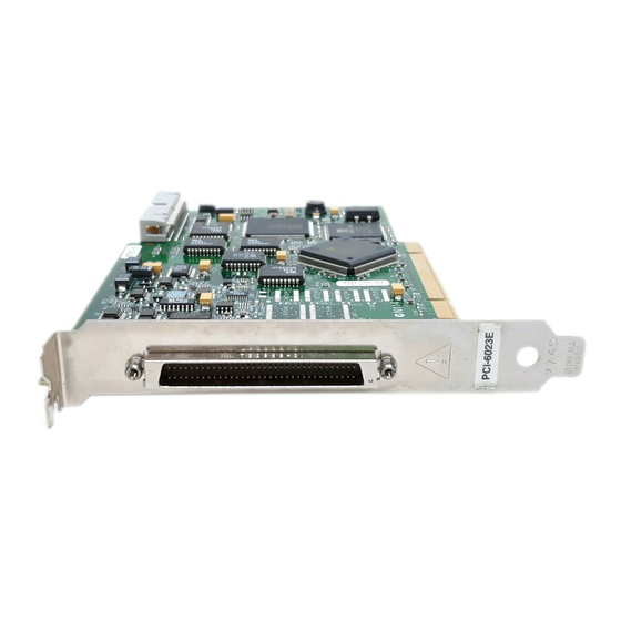
PCI-6023E/6024E/6025E User Manual Multifunction I/O Boards for PCI Bus Computers PCI-6023E/6024E/6025E User Manual October 1998 Edition Part Number 322072A-01... - Page 2 Singapore 2265886, Spain 91 640 0085, Sweden 08 730 49 70, Switzerland 056 200 51 51, Taiwan 02 377 1200, United Kingdom 01635 523545 National Instruments Corporate Headquarters 6504 Bridge Point Parkway Austin, Texas 78730-5039 USA Tel: 512 794 0100 © Copyright 1998 National Instruments Corporation. All rights reserved.
-
Page 3: Important Information
The PCI-6023E, PCI-6024E, and PCI-6025E boards are warranted against defects in materials and workmanship for a period of one year from the date of shipment, as evidenced by receipts or other documentation. National Instruments will, at its option, repair or replace equipment that proves to be defective during the warranty period. This warranty includes parts and labor. -
Page 4: Table Of Contents
National Instruments Documentation ...xiii Related Documentation...xiv Customer Communication ...xiv Chapter 1 Introduction Features of the PCI-6023E, PCI-6024E, and PCI-6025E ...1-1 What You Need to Get Started ...1-2 Unpacking ... 1-2 Software Programming Choices ...1-3 National Instruments Application Software ...1-3 NI-DAQ Driver Software ...1-3 Register-Level Programming ...1-5... - Page 5 Timing Connections ... 4-30 Programmable Function Input Connections ... 4-31 DAQ Timing Connections ... 4-32 SCANCLK Signal ... 4-33 EXTSTROBE* Signal ... 4-33 TRIG1 Signal... 4-34 TRIG2 Signal... 4-35 STARTSCAN Signal... 4-36 CONVERT* Signal ... 4-38 PCI-6023E/6024E/6025E User Manual © National Instruments Corporation...
- Page 6 Chapter 5 Calibration Loading Calibration Constants ...5-1 Self-Calibration...5-2 External Calibration ...5-2 Other Considerations ...5-3 Appendix A Specifications Appendix B Custom Cabling and Optional Connectors Appendix C Common Questions Appendix D Customer Communication © National Instruments Corporation PCI-6023E/6024E/6025E User Manual Contents...
- Page 7 CONVERT* Signal Routing... 3-7 Figure 3-4. RTSI Bus Signal Connection ... 3-9 Figure 4-1. I/O Connector Pin Assignment for the PCI-6023E/PCI-6024E ... 4-2 Figure 4-2. I/O Connector Pin Assignment for the PCI-6025E... 4-3 Figure 4-3. Programmable Gain Instrumentation Amplifier (PGIA) ... 4-10 Figure 4-4.
- Page 8 Measurement Precision ...3-3 Table 4-1. I/O Connector Signal Descriptions ...4-4 Table 4-2. I/O Signal Summary ...4-7 Table 4-3. Port C Signal Assignments ...4-23 Table 4-4. Signal Names Used in Timing Diagrams ...4-25 © National Instruments Corporation PCI-6023E/6024E/6025E User Manual Contents...
-
Page 9: About This Manual
I/O, and timing I/O. This manual describes the electrical and mechanical aspects of the PCI-6023E, PCI-6024E, and PCI-6025E boards from the PCI E Series product line and contains information concerning their operation and programming. -
Page 10: Conventions Used In This Manual
NI-DAQ refers to the NI-DAQ driver software for PC compatible computers unless otherwise noted. Refers to all PC AT series computers with PCI bus unless otherwise noted. PCI-6023E/6024E/6025E User Manual Index contains an alphabetical list of key terms and topics in this manual, including the page where you can find each one. -
Page 11: National Instruments Documentation
SCXI SCXI stands for Signal Conditioning eXtensions for Instrumentation and is a National Instruments product line designed to perform front-end signal conditioning for National Instruments plug-in DAQ boards. National Instruments Documentation The PCI-6023E/6024E/6025E User Manual is one piece of the documentation set for your DAQ system. -
Page 12: Related Documentation
• Customer Communication National Instruments wants to receive your comments on our products and manuals. We are interested in the applications you develop with our products, and we want to help if you have problems with them. To make it easy for you to contact us, this manual contains comment and configuration forms for you to complete. -
Page 13: Introduction
32 lines of digital I/O. The PCI-6024E features 16 channels of analog input, two channels of analog output, a 68-pin connector and eight lines of digital I/O. The PCI-6023E is identical to the PCI-6024E, except that it does not have analog output channels. -
Page 14: What You Need To Get Started
Remove the board from the package and inspect the board for loose components or any other sign of damage. Notify National Instruments if the board appears damaged in any way. Do not install a damaged board into your computer. Never touch the exposed pins of connectors. -
Page 15: Software Programming Choices
Software Programming Choices You have several options to choose from when programming your National Instruments DAQ and SCXI hardware. You can use National Instruments application software, NI-DAQ, or register-level programming. National Instruments Application Software ComponentWorks contains tools for data acquisition and instrument control built on NI-DAQ driver software. - Page 16 An example of a low-level function is writing directly to registers on the DAQ device. NI-DAQ does not sacrifice the performance of National Instruments DAQ devices because it lets multiple devices operate at their peak.
-
Page 17: Register-Level Programming
Register-Level Programming The final option for programming any National Instruments DAQ hardware is to write register-level software. Writing register-level programming software can be very time-consuming and inefficient, and is not recommended for most users. Even if you are an experienced register-level programmer, using NI-DAQ... -
Page 18: Optional Equipment
Chapter 1 Introduction Optional Equipment National Instruments offers a variety of products to use with your board, including cables, connector blocks, and other accessories, as follows: • • • • • For more specific information about these products, refer to your National Instruments catalogue or call the office nearest you. -
Page 19: Installation And Configuration
Installation and Configuration This chapter explains how to install and configure your PCI-6023E, PCI-6024E, or PCI-6025E board. Software Installation Install your software before you install your board. Refer to the appropriate release notes indicated below for specific instructions on the software installation sequence. -
Page 20: Hardware Installation
PCI-6023E/6024E/6025E User Manual Hardware Overview, for more information about the various Write down your board’s serial number in the PCI-6023E/6024E/6025E Hardware and Software Configuration Form in Appendix D, this manual. Turn off and unplug your computer. -
Page 21: Hardware Overview
Hardware Overview This chapter presents an overview of the hardware functions on your board. Figure 3-1 shows a block diagram for the PCI-6023E, PCI-6024E, and PCI-6025E. Voltage Analog Analog Mode Input Multiplexer Muxes Dither Calibration Generator PFI / Trigger Timing... -
Page 22: Table 3-1. Available Input Configurations
For diagrams showing the signal paths of the three configurations, refer to Connections. Input Range The PCI-6023E, PCI-6024E, and PCI-6025E boards have a bipolar input range that changes with the programmed gain. Each channel may be programmed with a unique gain of 0.5, 1.0, 10, or 100 to maximize the PCI-6023E/6024E/6025E User Manual Table 3-1. -
Page 23: Table 3-2. Measurement Precision
Figure 3-2d, eliminates both the added noise and the effects of quantization. Dither has the effect of forcing quantization noise to become a zero-mean random variable rather than a deterministic function of the input signal. © National Instruments Corporation Table 3-2. Measurement Precision Gain Input Range... -
Page 24: Multichannel Scanning Considerations
Dither enabled; no averaging Multichannel Scanning Considerations The PCI-6023E, PCI-6024E, and PCI-6025E boards can scan multiple channels at the same maximum rate as their single-channel rate; however, pay careful attention to the settling times for each of the boards. No extra settling time is necessary between channels as long as the gain is constant and source impedances are low. -
Page 25: Analog Output
In normal operation, a DAC output will glitch whenever it is updated with a new value. The glitch energy differs from code to code and appears as distortion in the frequency spectrum. © National Instruments Corporation Chapter 3 PCI-6023E/6024E/6025E User Manual... -
Page 26: Digital I/O
Chapter 3 Hardware Overview Digital I/O The PCI-6023E, PCI-6024, and PCI-6025E boards contain eight lines of digital I/O (DIO<0..7>) for general-purpose use. You can individually software-configure each line for either input or output. At system startup and reset, the digital I/O ports are all high impedance. -
Page 27: Programmable Function Inputs
I/O connector for different applications. You can also individually enable each of the PFI pins to output a specific internal timing signal. For example, if you need the © National Instruments Corporation Chapter 3 Figure 3-3. CONVERT* Signal Routing... -
Page 28: Board And Rtsi Clocks
PCI E Series board sharing the RTSI bus. These bidirectional lines can drive any of eight timing signals onto the RTSI bus and can receive any of these timing signals. This signal connection scheme is shown in Figure 3-4. PCI-6023E/6024E/6025E User Manual © National Instruments Corporation... -
Page 29: Figure 3-4. Rtsi Bus Signal Connection
Refer to the for a description of the signals shown in Figure 3-4. © National Instruments Corporation Trigger Clock switch Figure 3-4. RTSI Bus Signal Connection Timing Connections section of Chapter 4, Chapter 3 Hardware Overview DAQ-STC TRIG1 TRIG2 CONVERT*... -
Page 30: Signal Connections
Maximum input ratings for each signal are given in the Protection column of Table 4-2. National Instruments is © National Instruments Corporation Connectors, for pin assignments of the optional liable for any damages resulting from such signal connections. -
Page 31: Figure 4-1. I/O Connector Pin Assignment For The Pci-6023E/Pci-6024E
PFI1/TRIG2 DGND +5 V DGND PFI5/UPDATE* PFI6/WFTRIG DGND PFI9/GPCTR0_GATE GPCTR0_OUT FREQ_OUT Not available on the PCI-6023E Figure 4-1. I/O Connector Pin Assignment for the PCI-6023E/PCI-6024E 34 68 ACH0 33 67 AIGND 32 66 ACH9 31 65 ACH2 30 64 AIGND... -
Page 32: Figure 4-2. I/O Connector Pin Assignment For The Pci-6025E
© National Instruments Corporation AIGND AIGND ACH0 ACH8 ACH1 ACH9 ACH2 ACH10 ACH3 ACH11 ACH4 ACH12 ACH5 ACH13 ACH6 ACH14 ACH7 ACH15 AISENSE DAC0OUT DAC1OUT RESERVED AOGND DGND DIO0 DIO4 DIO1 DIO5 DIO2 DIO6 DIO3 DIO7 DGND +5 V +5 V... -
Page 33: Table 4-1. I/O Connector Signal Descriptions
Chapter 4 Signal Connections Table 4-1 shows the I/O connector signal descriptions for the PCI-6023E, PCI-6024E, and PCI-6025E. Signal Name Reference AIGND ACH<0..15> AIGND AISENSE AIGND DAC0OUT AOGND DAC1OUT AOGND AOGND DGND DIO<0..7> DGND PA<0..7> DGND PB<0..7> DGND PC<0..7> DGND... - Page 34 PFI3/GPCTR1_SOURCE DGND PFI4/GPCTR1_GATE DGND GPCTR1_OUT DGND © National Instruments Corporation Direction Output Scan Clock—This pin pulses once for each A/D conversion in scanning mode when enabled. The low-to-high edge indicates when the input signal can be removed from the input or switched to another signal.
- Page 35 GPCTR0_OUT DGND FREQ_OUT DGND Indicates that the signal is active low Not available on the PCI-6023E Not available on the PCI-6023E or PCI-6024E PCI-6023E/6024E/6025E User Manual Direction Input PFI5/Update—As an input, this is one of the PFIs. Output As an output, this is the UPDATE* (AO Update) signal. A...
-
Page 36: Table 4-2. I/O Signal Summary
Table 4-2 shows the I/O signal summary for the PCI-6023E, PCI-6024E, and PCI-6025E. Signal Type and Signal Name Direction ACH<0..15> AISENSE AIGND DAC0OUT (6024E and 6025E only) DAC1OUT (6024E and 6025E only) AOGND DGND DIO<0..7> PA<0..7> (6025E only) PB<0..7> (6025E only) PC<0..7>... -
Page 37: Analog Input Signal Overview
Input Signal Types of Signal Sources When configuring the input channels and making signal connections, you must first determine whether the signal sources are floating or ground-referenced. PCI-6023E/6024E/6025E User Manual Table 4-2. I/O Signal Summary (Continued) Impedance Protection Input/ (Volts) -
Page 38: Floating Signal Sources
(NRSE), referenced single ended (RSE), and differential (DIFF). With the different configurations, you can use the PGIA in different ways. Figure 4-3 shows a diagram of your board’s PGIA. © National Instruments Corporation Chapter 4 PCI-6023E/6024E/6025E User Manual... -
Page 39: Figure 4-3. Programmable Gain Instrumentation Amplifier (Pgia)
Exceeding the differential and common-mode input ranges distorts your input signals. Exceeding the maximum input voltage rating can damage the board and the computer. National Instruments is such signal connections. The maximum input voltage ratings are listed in the Protection column of Table 4-2. -
Page 40: Analog Input Signal Connections
Figure 4-4 summarizes the recommended input configuration for both types of signal sources. © National Instruments Corporation Chapter 4 Differential Connections for Nonreferenced or section in this chapter). If you have a grounded... -
Page 41: Figure 4-4. Summary Of Analog Input Connections
See text for information on bias resistors. Single-Ended — Ground Referenced (RSE) Single-Ended — Nonreferenced (NRSE) See text for information on bias resistors. PCI-6023E/6024E/6025E User Manual Signal Source Type Floating Signal Source ACH(+) ACH (-) AIGND AIGND AISENSE AIGND Figure 4-4. Summary of Analog Input Connections... -
Page 42: Differential Connection Considerations (Diff Input Configuration)
Differential signal connections also allow input signals to float within the common-mode limits of the PGIA. © National Instruments Corporation The input signal is low level (less than 1 V). The leads connecting the signal to the board are greater than 10 ft (3 m). -
Page 43: Differential Connections For Ground-Referenced Signal Sources
I/O Connector With this type of connection, the PGIA rejects both the common-mode noise in the signal and the ground potential difference between the signal source and the board ground, shown as V PCI-6023E/6024E/6025E User Manual ACH+ ACH- Input Multiplexers... -
Page 44: Differential Connections For Nonreferenced Or Floating Signal Sources
PGIA. The PGIA will then saturate, causing erroneous readings. You must reference the source to AIGND. The easiest way is to connect the positive side of the signal to the positive input © National Instruments Corporation ACH+ ACH-... - Page 45 PCI-6023E/6024E/6025E User Manual 4-16 © National Instruments Corporation...
-
Page 46: Single-Ended Connection Considerations
© National Instruments Corporation The input signal is high level (greater than 1 V). The leads connecting the signal to the board are less than 10 ft (3 m). -
Page 47: Single-Ended Connections For Floating Signal Sources (Rse Configuration)
If the input circuitry of a board were referenced to ground, in this situation as in the RSE input configuration, this difference in ground potentials would appear as an error in the measured voltage. PCI-6023E/6024E/6025E User Manual Input Multiplexers AISENSE... -
Page 48: Common-Mode Signal Rejection Considerations
PGIA can reject common-mode noise pickup in the leads connecting the signal sources to the board. The PGIA can reject common-mode signals as long as V+ within ±11 V of AIGND. © National Instruments Corporation ACH+ ACH- Input Multiplexers... -
Page 49: Analog Output Signal Connections
PCI-6024E and PCI-6025E The analog output signals are DAC0OUT, DAC1OUT, and AOGND. DAC0OUT and DAC1OUT are not available on the PCI-6023E. DAC0OUT is the voltage output signal for analog output channel 0. DAC1OUT is the voltage output signal for analog output channel 1. -
Page 50: Digital I/O Signal Connections
Figure 4-10 shows DIO<0..3> configured for digital input and DIO<4..7> configured for digital output. Digital input applications include receiving TTL signals and sensing external device states such as the state of the © National Instruments Corporation TTL Signal DGND I/O Connector Figure 4-10. -
Page 51: Pci-6025E Only
Figure 4-11 depicts signal connections for three typical digital I/O applications. +5 V +5 V Switch I/O Connector PCI-6023E/6024E/6025E User Manual TTL Signal Figure 4-11. Digital I/O Connections Block Diagram 4-22 Port A PA<3..0> Port B PB<7..4>... -
Page 52: Table 4-3. Port C Signal Assignments
Mode 2 Handshaking (Bidirectional Bus) *Indicates that the signal is active low. Subscripts A and B denote port A or port B handshaking signals. © National Instruments Corporation Table 4-3. Port C Signal Assignments Signal Assignments 4-23 Chapter 4 Signal Connections... -
Page 53: Digital I/O Power-Up State
A given DIO line is pulled high at power up. To pull it low on power up with an external resistor, follow these steps: PCI-6023E/6024E/6025E User Manual (approximately +5 VDC) with a 100 k ) whose value will give you a maximum of 0.4... -
Page 54: Table 4-4. Signal Names Used In Timing Diagrams
Name Type STB* Input Output © National Instruments Corporation Using the following formula, calculate the largest possible load to maintain a logic low level of 0.4 V and supply the maximum driving current: V = I * R = V/I, where: V = 0.4 V... - Page 55 Internal Internal DATA Bidirectional PCI-6023E/6024E/6025E User Manual Description Acknowledge Input—A low signal on this handshaking line indicates that the data written to the port has been accepted. This signal is a response from the external device indicating that it has received the data from your DIO board.
-
Page 56: Mode 1 Input Timing
Data after STB* = 1 RD* = 0 to INTR = 0 RD* = 1 to IBF = 0 All timing values are in nanoseconds. © National Instruments Corporation Description Figure 4-13. Timing Specifications for Mode 1 Input Transfer 4-27... -
Page 57: Mode 1 Output Timing
WR* = 1 to OBF* = 0 ACK* = 0 to OBF* = 1 ACK* Pulse Width ACK* = 1 to INTR = 1 All timing values are in nanoseconds. PCI-6023E/6024E/6025E User Manual Description Figure 4-14. Timing Specifications for Mode 1 Output Transfer 4-28 Minimum Maximum —... -
Page 58: Mode 2 Bidirectional Timing
ACK* = 0 to Output ACK* = 1 to Output Float RD* = 1 to IBF = 0 All timing values are in nanoseconds. © National Instruments Corporation Description Figure 4-15. Timing Specifications for Mode 2 Bidirectional Transfer 4-29 Chapter 4... -
Page 59: Power Connections
Under no circumstances should you connect these +5 V power pins directly to analog or digital ground or to any other voltage source on the board or any other device. Doing so can damage the board and the computer. National Instruments liable for damages resulting from such a connection. -
Page 60: Programmable Function Input Connections
As an input, you can individually configure each PFI pin for edge or level detection and for polarity selection, as well. You can use the polarity selection for any of the 13 timing signals, but the edge or level detection © National Instruments Corporation Source I/O Connector Figure 4-16. -
Page 61: Daq Timing Connections
Figure 4-18 shows a typical pretriggered DAQ sequence. The description for each signal shown in these figures is included later in this chapter. STARTSCAN Scan Counter PCI-6023E/6024E/6025E User Manual TRIG1 CONVERT* Figure 4-17. Typical Posttriggered Acquisition 4-32... -
Page 62: Scanclk Signal
A 10 µs and a 1.2 µs clock are available for generating a sequence of eight pulses in the hardware-strobe mode. Figure 4-20 shows the timing for the hardware-strobe mode EXTSTROBE* signal. © National Instruments Corporation Figure 4-18. Typical Pretriggered Acquisition CONVERT* SCANCLK Figure 4-19. -
Page 63: Trig1 Signal
Figures 4-21 and 4-22 show the input and output timing requirements for the TRIG1 signal. Rising-edge polarity Falling-edge polarity PCI-6023E/6024E/6025E User Manual V OH V OL = 600 ns or 5 s Figure 4-20. EXTSTROBE* Signal Timing = 10 ns minimum Figure 4-21. -
Page 64: Trig2 Signal
PFI. The TRIG2 signal is not used in posttriggered data acquisition. The output is an active high pulse with a pulse width of 50 to 100 ns. This output is set to tri-state at startup. © National Instruments Corporation 4-35 PCI-6023E/6024E/6025E User Manual... -
Page 65: Startscan Signal
The second action is an active high pulse that terminates at the start of the last conversion in the scan, which indicates a scan in progress. PCI-6023E/6024E/6025E User Manual = 10 ns minimum Figure 4-23. TRIG2 Input Signal Timing = 50-100 ns Figure 4-24. -
Page 66: Figure 4-25. Startscan Input Signal Timing
If you select an external CONVERT*, the first external pulse after STARTSCAN generates a conversion. The STARTSCAN pulses should be separated by at least one scan period. © National Instruments Corporation = 10 ns minimum Figure 4-25. STARTSCAN Input Signal Timing = 50-100 ns a. -
Page 67: Convert* Signal
50 to 150 ns. This output is set to tri-state at startup. Figures 4-27 and 4-28 show the input and output timing requirements for the CONVERT* signal. Rising-edge polarity Falling-edge polarity PCI-6023E/6024E/6025E User Manual = 10 ns minimum Figure 4-27. CONVERT* Input Signal Timing 4-38 © National Instruments Corporation... -
Page 68: Aigate Signal
AIGATE does not gate them back on until the beginning of the next scan. © National Instruments Corporation 4-39 PCI-6023E/6024E/6025E User Manual... -
Page 69: Sisource Signal
(UI) counter is started if you select internally generated UPDATE*. As an output, the WFTRIG signal reflects the trigger that initiates waveform generation. This is true even if the waveform generation is being PCI-6023E/6024E/6025E User Manual = 50 ns minimum = 23 ns minimum Figure 4-29. -
Page 70: Update* Signal
PFI. The output is an active low pulse with a pulse width of 300 to 350 ns. This output is set to tri-state at startup. © National Instruments Corporation = 10 ns minimum Figure 4-30. WFTRIG Input Signal Timing = 50-100 ns Figure 4-31. -
Page 71: Uisource Signal
UISOURCE signal in the level-detection mode. You can configure the polarity selection for the PFI pin for either active high or active low. Figure 4-34 shows the timing requirements for the UISOURCE signal. PCI-6023E/6024E/6025E User Manual = 10 ns minimum Figure 4-32. UPDATE* Input Signal Timing = 300-350 ns Figure 4-33. -
Page 72: General-Purpose Timing Signal Connections
This output is set to tri-state at startup. Figure 4-35 shows the timing requirements for the GPCTR0_SOURCE signal. © National Instruments Corporation Chapter 4 = 50 ns minimum = 23 ns minimum Figure 4-34. UISOURCE Signal Timing... -
Page 73: Gpctr0_Gate Signal
0. This is true even if the gate is being externally generated by another PFI. This output is set to tri-state at startup. PCI-6023E/6024E/6025E User Manual = 50 ns minimum = 23 ns minimum Figure 4-35. GPCTR0_SOURCE Signal Timing 4-44 ©... - Page 74 You can disable this input so that software can control the up-down functionality and leave the DIO6 pin free for general use. © National Instruments Corporation = 10 ns minimum Figure 4-36. GPCTR0_GATE Signal Timing in Edge-Detection Mode Figure 4-37.
-
Page 75: Gpctr1_Source Signal
PCI-6023E/6024E/6025E User Manual = 50 ns minimum = 23 ns minimum Figure 4-38. GPCTR1_SOURCE Signal Timing 4-46 ©... - Page 76 This input can be disabled so that software can control the up-down functionality and © National Instruments Corporation = 10 ns minimum Figure 4-39. GPCTR1_GATE Signal Timing in Edge-Detection Mode Figure 4-40.
- Page 77 If you use an internal timebase clock, the gate signal cannot be synchronized with the clock. In this case, gates applied close to a source edge take effect either on that source edge or on the next one. This PCI-6023E/6024E/6025E User Manual Source Clock Period Source Pulse Width...
-
Page 78: Freq_Out Signal
• • • © National Instruments Corporation Use differential analog input connections to reject common-mode noise. Use individually shielded, twisted-pair wires to connect analog input signals to the board. With this type of wire, the signals attached to the CH+ and CH–... - Page 79 • • For more information, refer to the application note, Field Wiring and Noise Consideration for Analog Signals, available from National Instruments. PCI-6023E/6024E/6025E User Manual Separate board signal lines from high-current or high-voltage lines. These lines can induce currents in or voltages on the board signal lines if they run in parallel paths at a close distance.
-
Page 80: Calibration
CalDACs with values either from the original factory calibration or from a calibration that you subsequently performed. This method of calibration is not very accurate because it does not take into account the fact that the board measurement and output voltage errors can © National Instruments Corporation PCI-6023E/6024E/6025E User Manual... -
Page 81: Self-Calibration
Self-Calibration Your board can measure and correct for almost all of its calibration-related errors without any external signal connections. Your National Instruments software provides a self-calibration method. This self-calibration process, which generally takes less than a minute, is the preferred method of assuring accuracy in your application. -
Page 82: Other Considerations
In this case, it is advisable to account for the nominal gain error of the analog output channel either in software or with external hardware. See Appendix A, Specifications, for analog output gain error information. © National Instruments Corporation PCI-6023E/6024E/6025E User Manual Chapter 5 Calibration... -
Page 83: Appendix A Specifications
Specifications This appendix lists the specifications of PCI-6023E, PCI-6024E, and PCI-6025E boards. These specifications are typical at 25° C unless otherwise noted. Analog Input Input Characteristics Number of channels ... 16 single-ended or 8 differential Type of ADC... Successive approximation Resolution ... - Page 84 Note: Accuracies are valid for measurements following an internal E Series Calibration. Averaged numbers assume dithering and averaging of 100 single-channel readings. Measurement accuracies are listed for operational temperatures within ± 1 °C of internal calibration temperature and ± 10 °C of external or factory calibration temperature. PCI-6023E/6024E/6025E User Manual Powered On ± 42 ±...
- Page 85 Input bias current ... ±200 pA Input offset current... ±100 pA CMRR (DC to 60 Hz) © National Instruments Corporation Pregain error after calibration ... ±12 V max Pregain error before calibration ... ±28 mV max Postgain error after calibration ... ±0.5 mV max Postgain error before calibration...
-
Page 86: Dynamic Characteristics
Gain temperature coefficient ...±20 ppm/°C Analog Output (PCI-6024E and PCI-6025E only) Output Characteristics Number of channels...2 voltage Resolution ...12 bits, 1 in 4,096 Max update rate ...100 kHz, system dependent PCI-6023E/6024E/6025E User Manual Signal Gain Dither Off Pregain...±15 µV/°C Postgain ...±240 µV/°C Bandwidth... -
Page 87: Accuracy Information
DMA modes... Scatter-gather Accuracy Information Transfer Characteristics Relative accuracy (INL) Monotonicity... 12 bits, guaranteed after Offset error Gain error (relative to internal reference) © National Instruments Corporation Nominal Range (V) Positive Negative 24 Hours –10 0.0177 After calibration ... ± 0.3 LSB typ, ± 0.5 LSB max Before calibration ... -
Page 88: Voltage Output
Offset temperature coefficient ...± 50 µV/°C Gain temperature coefficient ...±25 ppm /°C Digital I/O Number of channels Compatibility ...TTL/CMOS PCI-6023E/6024E/6025E User Manual Magnitude ... Duration... 2.0 µs PCI-6025E ...32 input/output PCI-6023E and PCI-6024E ...8 input/output ± 12 mV © National Instruments Corporation... - Page 89 Input low current (V Input high current (V Output low voltage (I Output high voltage (I Handshaking... 2-wire Power-on state PA<0..7> ... Input (High-Z), © National Instruments Corporation Appendix A Level = 0 V) = 5 V) = 24 mA) = 13 mA)
-
Page 90: Digital Trigger
Data transfers ...DMA, interrupts, programmed DMA modes ...Scatter-gather Triggers Digital Trigger Compatibility ...TTL Response ...Rising or falling edge PCI-6023E/6024E/6025E User Manual Counter/timers ...24 bits Frequency scalers ...4 bits Counter/timers ...20 MHz, 100 kHz Frequency scalers ...10 MHz, 100 kHz 100 k pull up to... -
Page 91: Operating Environment
© National Instruments Corporation Level ... 5.000 V (±3.5 mV) (actual Temperature coefficient ... ±5 ppm/°C max Long-term stability ... ±15 ppm/ PCI-6023E/6024E ... 68-pin male SCSI-II type PCI-6025E ... 100-pin female 0.05D type Appendix A Specifications value stored in EEPROM) -
Page 92: Custom Cabling
This appendix describes the various cabling and connector options for the boards. Custom Cabling National Instruments offers cables and accessories for you to prototype your application or to use if you frequently change board interconnections. If you want to develop your own cable, however, the following guidelines may be useful: •... -
Page 93: Optional Connectors
Figure B-1 shows the pin assignments for the 68-pin E Series connector. This connector is available when you use the SH6868 or R6868 cable assemblies with the PCI-6023E and PCI-6024E. It is also the MIO-16 68-pin connector available when you use the SH1006868 cable assembly with the PCI-6025E. -
Page 94: Figure B-1. 68-Pin E Series Connector Pin Assignments
PFI1/TRIG2 10 44 DGND +5 V DGND PFI5/UPDATE* PFI6/WFTRIG DGND PFI9/GPCTR0_GATE GPCTR0_OUT FREQ_OUT Not available on the PCI-6023E Figure B-1. 68-Pin E Series Connector Pin Assignments Custom Cabling and Optional Connectors ACH0 AIGND ACH9 ACH2 AIGND ACH11 AISENSE ACH12 ACH5... -
Page 95: Figure B-2. 68-Pin Extended Digital Input Connector Pin Assignments
Custom Cabling and Optional Connectors Figure B-2 shows the pin assignments for the 68-pin extended digital input connector. This is the other 68-pin connector available when you use the SH1006868 cable assembly with the PCI-6025E. PCI-6023E/6024E/6025E User Manual 34 68 33 67 32 66... -
Page 96: Figure B-3. 50-Pin E Series Connector Pin Assignments
Figure B-3 shows the pin assignments for the 50-pin E Series connector. This connector is available when you use the SH6850 or R6850 cable assemblies with the PCI-6023E and PCI-6024E. It is also one of the two 50-pin connectors available when you use the RI005050 cable assembly with the PCI-6025E. -
Page 97: Figure B-4. 50-Pin Extended Digital Input Connector Pin Assignments
Custom Cabling and Optional Connectors Figure B-4 shows the pin assignments for the 50-pin extended digital input connector. This is the other 50-pin connector available when you use the R1005050 cable assembly with the PCI-6025E. PCI-6023E/6024E/6025E User Manual 11 12 13 14 15 16... -
Page 98: General Information
What is the DAQ-STC? The DAQ-STC is the System Timing Control application-specific integrated circuit (ASIC) designed by National Instruments and is the backbone of the PCI E Series boards. The DAQ-STC contains seven 24-bit counters and three 16-bit counters. The counters are divided into the following three groups: •... -
Page 99: Installation And Configuration
What jumpers should I be aware of when configuring my PCI E Series board? The PCI E Series boards are jumperless and switchless. Which National Instruments document should I read first to get started using DAQ software? Your NI-DAQ or application software release notes documentation is always the best starting place. - Page 100 CTR VIs will still run. However, there are many differences in the counters between the PCI E Series and other boards; the counter numbers are different, timebase selections are different, and the DAQ-STC counters © National Instruments Corporation Enable the PFI5 line for output, as follows: •...
- Page 101 At system power-on and reset, both the PFI and DIO lines are set to high impedance by the hardware. This means that the board circuitry is not actively driving the output either high or low. However, these lines PCI-6023E/6024E/6025E User Manual call in NI-DAQ to configure the output line. By Select_Signal...
- Page 102 Table 4-2 shows that there is a 50 k pull-up resistor. This pull-up resistor will set the DIO(0) pin to a logic high when the output is in a high impedance state. © National Instruments Corporation PCI-6023E/6024E/6025E User Manual...
-
Page 103: Customer Communication
Electronic Services Bulletin Board Support National Instruments has BBS and FTP sites dedicated for 24-hour support with a collection of files and documents to answer most common customer questions. From these sites, you can also download the latest instrument drivers, updates, and example programs. For recorded instructions on how to use the bulletin board and FTP services and for BBS automated information, call 512 795 6990. -
Page 104: Telephone And Fax Support
Telephone and Fax Support National Instruments has branch offices all over the world. Use the list below to find the technical support number for your country. If there is no National Instruments office in your country, contact the source from which you purchased your software to obtain support. -
Page 105: Technical Support Form
National Instruments for technical support helps our applications engineers answer your questions more efficiently. If you are using any National Instruments hardware or software products related to this problem, include the configuration forms from their user manuals. Include additional pages if necessary. -
Page 106: Other Products
Complete a new copy of this form each time you revise your software or hardware configuration, and use this form as a reference for your current configuration. Completing this form accurately before contacting National Instruments for technical support helps our applications engineers answer your questions more efficiently. -
Page 107: Documentation Comment Form
Documentation Comment Form National Instruments encourages you to comment on the documentation supplied with our products. This information helps us provide quality products to meet your needs. Title: PCI-6023E/6024E/6025E User Manual Edition Date: October 1998 Part Number: 322072A-01 Please comment on the completeness, clarity, and organization of the manual. - Page 108 – negative of, or minus ° degree amperes alternating current AC coupled allowing the transmission of AC signals while blocking DC signals analog input channel signal © National Instruments Corporation Value –12 –9 – 6 –3 PCI-6023E/6024E/6025E User Manual...
- Page 109 PCI-6023E/6024E/6025E User Manual © National Instruments Corporation...
- Page 110 CMRR common-mode rejection ratio—a measure of an instrument’s ability to reject interference from a common-mode signal, usually expressed in decibels (dB) cold-junction a method of compensating for inaccuracies in thermocouple circuits compensation © National Instruments Corporation PCI-6023E/6024E/6025E User Manual Glossary...
- Page 111 (2) collecting and measuring the same kinds of electrical signals with A/D and/or DIO boards plugged into a computer, and possibly generating control signals with D/A and/or DIO boards in the same computer PCI-6023E/6024E/6025E User Manual © National Instruments Corporation...
- Page 112 A/D conversion © National Instruments Corporation PCI-6023E/6024E/6025E User Manual Glossary...
- Page 113 GATE gate signal glitch an unwanted momentary deviation from a desired signal GPCTR general purpose counter GPCTR0_GATE general purpose counter 0 gate signal PCI-6023E/6024E/6025E User Manual © National Instruments Corporation...
- Page 114 I/O. hexadecimal hertz—the number of events per second inches integral nonlinearity—a measure in LSB of the worst-case deviation from the ideal A/D or D/A transfer characteristic of the analog I/O circuitry © National Instruments Corporation PCI-6023E/6024E/6025E User Manual Glossary...
- Page 115 1,000, or 10 measure such as volts, hertz, and meters kilo—the prefix for 1,024, or 2 computer memory 1,000 samples PCI-6023E/6024E/6025E User Manual , used with units of , used with B in quantifying data or © National Instruments Corporation...
- Page 116 NI-DAQ National Instruments driver software for DAQ hardware © National Instruments Corporation PCI-6023E/6024E/6025E User Manual Glossary...
- Page 117 132 Mbytes/s. peak to peak a measure of signal amplitude; the difference between the highest and lowest excursions of the signal programmable function input PCI-6023E/6024E/6025E User Manual G-10 © National Instruments Corporation...
-
Page 118: Programmable Gain Instrumentation Amplifier
DAQ board to keep a continuous buffer filled with data, so that when the trigger conditions are met, the sample includes the data leading up to the trigger condition points pullup © National Instruments Corporation G-11 PCI-6023E/6024E/6025E User Manual Glossary... - Page 119 Also called a grounded measurement system. PCI-6023E/6024E/6025E User Manual G-12 © National Instruments Corporation...
- Page 120 RTSI bus real-time system integration bus—the National Instruments timing bus that connects DAQ boards directly, by means of connectors on top of the boards, for precise synchronization of functions seconds samples sample counter the clock that counts the output of the channel clock, in other words, the number of samples taken.
- Page 121 (2) software—a property of a function that begins an operation and returns only when the operation is complete system noise a measure of the amount of noise seen by an analog circuit or an ADC when the analog inputs are grounded PCI-6023E/6024E/6025E User Manual G-14 © National Instruments Corporation...
- Page 122 For example, one pulse from the update clock produces one update which sends one new sample to every analog output channel in the group. update rate the number of output updates per second © National Instruments Corporation G-15 PCI-6023E/6024E/6025E User Manual Glossary...
- Page 123 See also breakdown voltage. PCI-6023E/6024E/6025E User Manual G-16 © National Instruments Corporation...
- Page 124 4-8 to 4-9 floating signal sources, 4-9 ground-referenced signal sources, 4-9 analog input modes, 4-8 to 4-19 © National Instruments Corporation available input configurations (table), 3-2 common-mode signal rejection considerations, 4-19 differential connections, 4-13 to 4-16...
- Page 125 CONVERT* signal DAQ timing connections, 4-38 to 4-39 signal routing (figure), 3-7 custom cabling, B-1 to B-2 customer communication, xiv, D-1 to D-2 PCI-6023E/6024E/6025E User Manual DAC0OUT signal analog output signal connections, 4-20 description (table), 4-4 signal summary (table), 4-7...
- Page 126 I/O specifications, A-7 signal summary (table), 4-7 dither, 3-3 to 3-4 documentation conventions used in manual, xii-xiii National Instruments documentation, xiii organization of manual, xi-xii related documentation, xiv e-mail support, D-2 EEPROM storage of calibration constants, 5-1 electronic support services, D-1 to D-2...
- Page 127 B-2 to B-6 50-pin E Series connector pin assignments (figure), B-5 50-pin extended digital input connector pin assignments (figure), B-6 PCI-6023E/6024E/6025E User Manual 68-pin E Series connector pin assignments (figure), B-3 68-pin extended digital input connector pin assignments (figure), B-4...
- Page 128 I/O specifications, A-7 to A-8 signal summary (table), 4-7 PC<0..7> signal description (table), 4-4 digital I/O specifications, A-7 to A-8 signal summary (table), 4-7 PCI-6023E/6024E/6025E. See also hardware overview. block diagram, 3-1 features, 1-1 optional equipment, 1-6 © National Instruments Corporation...
- Page 129 (figure), 4-18 ground-referenced signal sources (figure), 4-19 physical specifications, A-9 pin assignments PCI-6023E/6024E (figure), 4-2 PCI-6025E (figure), 4-3 Port C pin assignments description, 4-23 signal assignments (table), 4-23 posttriggered acquisition (figure), 4-32 power connections, 4-30...
- Page 130 4-40 to 4-43 timing specifications, 4-25 to 4-29 mode 1 input timing (figure), 4-27 mode 1 output timing (figure), 4-28 © National Instruments Corporation mode 2 bidirectional timing (figure), 4-29 signal names used in diagrams (table), 4-25 to 4-26...
- Page 131 (figure), 4-33 general-purpose timing signal connections, 4-43 to 4-49 FREQ_OUT signal, 4-49 GPCTR0_GATE signal, 4-44 to 4-45 GPCTR0_OUT signal, 4-45 PCI-6023E/6024E/6025E User Manual GPCTR0_SOURCE signal, 4-43 to 4-44 GPCTR0_UP_DOWN signal, 4-45 GPCTR1_GATE signal, 4-46 to 4-47 GPCTR1_OUT signal, 4-47 GPCTR1_UP_DOWN signal,...
- Page 132 UPDATE* signal, 4-41 to 4-42 WFTRIG signal, 4-40 to 4-41 WFTRIG signal, 4-40 to 4-41 WR* signal description (table), 4-26 mode 1 output timing (figure), 4-28 mode 2 bidirectional timing (figure), 4-29 © National Instruments Corporation PCI-6023E/6024E/6025E User Manual Index...
Need help?
Do you have a question about the DAQ PCI-6023E and is the answer not in the manual?
Questions and answers