Table of Contents
Advertisement
Quick Links
This service information is designed for experienced repair technicians only and is not designed for use by the general public.
It does not contain warnings or cautions to advise non-technical individuals of potential dangers in attempting to service a
product.
Products powered by electricity should be serviced or repaired only by experienced professional technicians. Any attempt to
service or repair the product or products dealt with in this service information by anyone else could result in serious injury or
death.
Revision : 03
Digital Cellular Telephone
900 MHz
Tx Frequency Range:
880 - 915MHz
Rx Frequency Range:
925 - 960 MHz
Tx / Rx separation
10.4 MHz
RF Channel Bandwidth
200 kHz
Number of RF channels
174
Speech coding
Full rate / Half rate / Enhanced Full rate
-10 °C to +55 °C
Operating temperature
Type
Class 4 Handheld
RF Output Power
2 W maximum
Modulation
GMSK (BT = 0.3)
Connection
8 ch / TDMA
Voice digitizing
13 kbps RPE-LTP / 13 kbps ACLEP / 5.6 kbps CELP / VSLEP
Transmission speed
27
Signal Reception
Direct conversion
Antenna VSWR
< 2.5 : 1
Height:
Dimensions
Width:
Depth: 17.85 mm (Depth excludes protrusions)
Volume
79 cc
Weight
102 g
Main Display
TFT LCD; approximately 16 million colours
Illumination
16 LEDs for Keypad Backlighting (14 Blue & 2 White)
4 LEDs for LCD Backlighting (White)
1 LEDs for Sub LCD (White)
Keys
21-key Keypad, Navigation key, 1 memo key
1.8 V & 3 V Plug-in type only
SIM
External DC Supply
5.8 V
Voltage
Battery
3.7 V nominal, 830 mAh, Li-Ion
3.7 V nominal, 810 mAh, Li-Ion for China market
Charging Time
150 minutes
Standby Time
up to 240 hrs
Talk Time
up to 5 hrss
Talk and standby time will be dependent on network conditions, SIM card, backlight usage
and network condition.
WARNING
2 0 0 5
P a n a s o n i c M o b i l e C o m m u n i c a t i o n s C o . , L t d .
A l l r i g h t s r e s e r v e d . U n a u t h o r i z e d c o p y i n g a n d
d i s t r i b u t i o n i s a v i o l a t i o n o f l a w .
ORDER NO. OMTD050601C8
EB-VS3
1800 MHz
1900 MHz
1710 -1785 MHz
1850 - 1910 MHz
1805 -1880 MHz
1930 - 1990 MHz
20.4 MHz
20.4 MHz
299
374
Class 1 Handheld
Class 1 Handheld
1 W maximum
1 W maximum
96 mm
46 mm
Advertisement
Table of Contents

Related Manuals for Panasonic EB-VS3


Summary of Contents for Panasonic EB-VS3
- Page 1 ORDER NO. OMTD050601C8 Digital Cellular Telephone EB-VS3 900 MHz 1800 MHz 1900 MHz Tx Frequency Range: 880 - 915MHz 1710 -1785 MHz 1850 - 1910 MHz Rx Frequency Range: 925 - 960 MHz 1805 -1880 MHz 1930 - 1990 MHz 20.4 MHz...
-
Page 2: Table Of Contents
The information contained in this manual and all rights in any design disclosed therein, are and remain the exclusive property of Panasonic Mobile Communications Co., Ltd. Other patents applying to material contained in this publication:... - Page 3 7. REPAIR PROCEDURES ............... . . 7-1 7.1.
- Page 4 ORDER NO. OMTD050601C8 Digital Cellular Telephone EB-VS3 VOL. 1 ........... .
-
Page 5: Introduction
They must not be incinerated, or disposed of as ordinary rubbish. 1.1. Purpose of the Manual This Service Manual contains the information and procedures required for installing, operating and servicing the Panasonic GSM Personal Cellular Mobile Telephone system operating on GSM Digital Cellular Networks. -
Page 6: General Description
2.2. Features The Panasonic Cellular Telephone Model EB-VS3 is a high performance, small, light, handset for business and domestic use. The following features are provided: Dual Codec, which includes Full Rate, Half Rate and Enhanced Full Rate (EFR) Speech Codec. -
Page 7: Operating Instructions
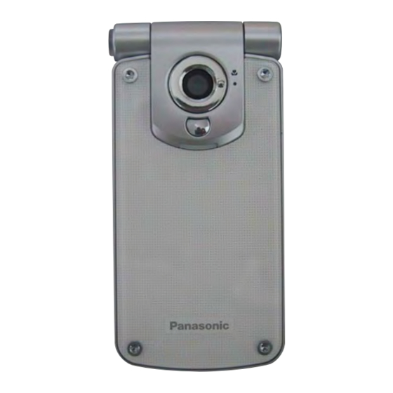
3. OPERATING INSTRUCTIONS 3.1. General This section provides a brief guide to the operation and facilities available on the telephone handset. Refer to the Operating Instructions supplied with the telephone for full operational information. 3.2. Phone Overview Earpiece Main Display Navigation Key One Push Auto Open Button Right Soft Key... -
Page 8: Key Functions
3.3. Key Functions Key Name Function Key Icon *1 Press outside edges to scroll up [i], down [o], left [4] or [i] [o] right [5] to move through menus and text. [4] [5] Navigation key Press centre [ ] to select to select option, or take a picture or record a video clip in Camera mode. -
Page 9: Quick Keys
3.4. Quick Keys Function In standby mode Open Main menu / Alert mute / Keyguard off Open Main menu Open Browser Short press [i] / [o] / [4] / [5] Open shortcut menu Open Call log ] / [ ] / [ Alert mute Keyguard on Dial your voice mailbox... -
Page 10: Display
3.5. Display Standby display Time Signal strength icon Date Battery charge level icon Wallpaper Left Soft key selection area Right Soft key selection area Status Icons Icon Meaning Signal strength; the more bars visible, the stronger the signal. In roaming area Battery charge level Battery is charging GPRS is active... -
Page 11: Menu Structure
3.6. Features Menu Structure Games Games Sound volume Settings Backlight Information Vibration Reset WAP profiles Picture Camera Video Alarms Tools Sound recorder Calculator Pictures My Media Sounds Videos Games Text templates Memory status MMS message Create new Messages SMS message Inbox Archive Call Voicemail... -
Page 12: Technical Specifications
4. TECHNICAL SPECIFICATIONS 4.1. Tx Characteristics All data is applicable to E-GSM 900 and GSM 1800 except where stated. Frequency Error ±0.1 ppm max., relative to base station frequency. Modulation Phase Error RMS: Equal to or less than 5 ° Peak: Equal to or less than 20 °... -
Page 13: Rx Characteristics
Spurious Emissions at Antenna Connector Limits (dBm) Frequency Filter Approx Frequency Range offset Bandwidth Video B/W E-GSM 900 GSM1800 − −36 −36 100 kHz to 50 MHz 10 kHz 30 kHz − −36 −36 50 MHz to 500 MHz 100 kHz 300 kHz −36 −36... - Page 14 GSM 1800 Full Rate Speech The reference sensitivity performance in terms of frame erasure, bit error, or residual bit error rates (whichever is appropriate) is specified in the following table, according to the propagation conditions. Channels Propagation Conditions Propagation Conditions Propagation Conditions Static Conditions TU high...
- Page 15 Blocking: Small MS level in dBµVemf( ) Frequency E-GSM 900 GSM 1800 FR ± 600 kHz to FR ± 800 kHz FR ± 800 kHz to FR± 1.6 MHz FR ± 1.6 MHz to FR ± 3 MHz 915 MHz to FR - 3 MHz –...
-
Page 16: Technical Description
ORDER NO. OMTD050601C8 Digital Cellular Telephone EB-VS3 VOL. 2 ......... . - Page 17 ORDER NO. OMTD050601C8 Digital Cellular Telephone EB-VS3 VOL. 3 ..... . . 6. DISASSEMBLY / REASSEMBLY INSTRUCTIONS ............
-
Page 18: Disassembly / Reassembly Instructions
6. DISASSEMBLY / REASSEMBLY INSTRUCTIONS 6.1. General This section provides disassembly and reassembly procedures for the main components of the telephone. These assemblies MUST be performed by qualified service personnel at an authorised service centre. The following Warnings and Cautions MUST be observed during all disassembly / reassembly operations: WARNING The equipment described in this manual contains polarised capacitors utilising liquid electrolyte. -
Page 19: Disassembly
6.2. Disassembly Lower Case Assembly and Main PCB removal 1. Place thumbs at outer edges of battery cover, press down, then slide the battery cover toward direction of the arrow. 2. Lift and remove battery. 3. Using tweezers, remove the two screw caps. Discard these items. Two screw caps. - Page 20 4. Use the Trident screwdriver to remove the four case screws. Retain the screws for re-use. Four case screws 5. Separate the two halves of the lower case assembly using a plastic strip (of Guitar pick thichness) as shown. 6. Remove the SIM/Speaker board by finger. SIM/Speaker PCB –...
- Page 21 7. Using tweezers, remove the hinge holder. Hindge holder 8. Carefully insert tweezers into the gap between FPC and Main PCB. 9. Gently lift up the tweezers direction of the arrow and then remove the FPC connector. 10.Remove Main PCB from the lower front cover. Note: Take care not to damage the FPC connector when disconnecting the FPC from the Main PCB.
- Page 22 3. Use the trident screwdriver to remove the four screws. Retain the screws for re-assembly Four screws 4. Set the phone into the "Close" position. 5. Use a strip of plastic (of guitar pick thickness) to separate the case halves. 6.
- Page 23 7. Set the phone to the "Open" position. 8. Using a small screw driver or tweezers, apply presure to the one push hinge direction while pulling the hinge away from the case. One push hinge 9. Lift and remove the case assembly. –...
- Page 24 LCD Removal 1. Using tweezers, carefully open the ZIF connector. 2. Remove four FPC from upper PCB. Caution: Lift up(open) or push down (close) flex lock crefully, If damaged, a new connector must be placed on PCB. ZIF connector 3. Peel the the adhesive tape and them remove the Upper PCB. Upper PCB Adhesive tape 4.
-
Page 25: Reassembly
6.3. Reassembly CAUTION IF ANY RF, BLUETOOTH OR BASEBAND SHIELDS ARE REMOVED FROM THE PCB AT ANY TIME, THEY MUST BE REPLACED WITH NEW ITEMS. ONCE REMOVED, THE SHIELDS MUST NOT BE REUSED. Notes: If the case assemblies have been disassembled and reassembled more than three times, they should be replaced with new items. - Page 26 5. Postion the camera macro switch and the case-mounted actuator so that they engage when the case halves are mated. Upper Cover Macro Mode Switch Upper Case Assembly 6. Place the Upper Case Assembly on the upper cover. Assemble the Upper Cover with the Upper Case Assembly. Close the four snaps making sure that both assemblies are connected.
- Page 27 9. Rotate and align the hinge pivot with the open area facing upward and carefuly insert the main area of the lower front cover, taking care to tilt the upper cover assembly without causing damege to the flex circuit during reassembly. 10.
- Page 28 15. Place the Main PCB on the lower front cover. 16. Connect the FPC connector on the Main PCB. 17. Connect the SIM PCB on the Main PCB. 18. Place the lower back case on the lower front cover. Fit the lower front cover to the lower back case. Close the four snaps making sure that both halves are connected.
-
Page 29: Repair Procedures
7. REPAIR PROCEDURES 7.1. Introduction This section describes the equipment and software required to test and calibrate the phone. Calibration Procedures are described in Section 8. The handset can be connected to a compatible personal computer for electronic adjustment and fault diagnosis. This section provides a description of the equipment required to perform those tasks. -
Page 30: Lead Free (Pbf) Solder
Re-flowing / Re-touching 1. Re-touching by soldering iron: HAKKO 928 soldering iron is recommended. 900S-T-B tip for thicker solder joints and 900M-T-LB tip for thinner solder joints are recommended. 2. Tip temperature/time Normal pad: 325 ± 10 °C, less than five seconds Large Pad: 400 ±... -
Page 31: Jigs And Tools
7.4. Jigs and Tools Personal Computer (PC) The PC (IBM compatible) is used as a Unit Under Test controller. This, in conjunction with the channel box software, allows all of the test facilities normally provided through the keypad of the Unit Under Test. The Microsoft Windows®... - Page 32 Dummy Battery with RF Test Jig (Part No. 3WZ001169AAA) Figure 5.2. : Dummy Battery with RF Test Jig Power Cable (Part No. 3WZ001130AAA) The power cable provides the necessary connections between the PCB repair jig / dummy battery and external power supply. Figure 5.3.
- Page 33 Calibrated Torque Screwdriver This screwdriver is required to secure the case screws on the phone. It must have settings for 1.3 kgf and 2.5 kgf. Power Supply Two power supplies is required to provide power to the PCB via the PCB Repair Jig while a second unit is required to provide power baseband calibration and unit testing.
- Page 34 ORDER NO. OMTD050601C8 Digital Cellular Telephone EB-VS3 VOL. 4 ......... . .
-
Page 35: Software Download
8. SOFTWARE DOWNLOAD 8.1. Flash Tool update and operation guide 8.1.1. Introduction The system has been tested on the following platforms: Windows ® 98, 2000, XP. System overview PC (with "Dongle") Phone serial port Headset Jack Stabilized Power Supply Voltage : 3.7 V NOTE : If using a battery pack to power the phone, ensure that it is fully charged. - Page 36 3. A notice is displayed warning the user to close down all other Windows applications. Close any open programs and then click "Next". 4. An information window is then displayed. When read, click "Next". 5. Flash Downloader will be installed under this folder by default. –...
- Page 37 6. Click "install" button. – 8-3 –...
- Page 38 7. The following screen is displayed. 8. Click "Install" button. Note: This driver is for using USB cable. 9. Click "Exit" button. Then installation of the Dongle driver will start automatically. 10. Select the language preference. Then click "OK" button. –...
- Page 39 11. Click "Next >" button. Then installation will start. – 8-5 –...
- Page 40 12. Click "Finish" button. Installation of the USB Cable Driver 1. Plug in the Dongle to the PC. 2. Connect the USB cable between the PC and handset. 3. Ensure that the handset is powerd OFF. 4. Short press the power key of handset. Note: Do not press &...
- Page 41 6. Following screen will be appeared. 7. Click "Continue Anyway" button. 8. Click "Finish" button. – 8-7 –...
- Page 42 Software Upgrade Procedure- FlashTool operation by using SPK file. Select [ Start ] - [ FlashTool ] - [ FlashTool_6_1 ] in PC menu. Then the following screen apperas. Click the tab of "Use SPK file". Select SPK file The following screen is displayed. Click "None"...
- Page 43 The following screen is displayed. Move to the folder where diffs is located Select spk file and press "Open" button. Then the path and name of .spk file are displayed. Then Click "OK". Check that all required files are in the same folder. COM port set-up The following screen is displayed –...
- Page 44 Each item can be changed by clicking the blue part. First COM port: Specify port number to connect the data cable. Number of COM ports : Number of actual machines to write. Normally one machine at a time, so 1 will be OK. Baud rate : When COM port is used on PC, enter 115200.
- Page 45 When download starts, progress bar is displayed. Do not disconnect the date cable while downloading. When download is successful, the following screen is displayed. – 8-11 –...
- Page 46 In case of an error, the following screen is displayed. If a download fails, check all connect ions between the phone, data cable and PC. Before restarting the download procedure , remove and then re-attach the phone battery. – 8-12 –...
-
Page 47: Calibration Procedure
9. CALIBRATION PROCEDURE 9.1. Introduction The following procedure MUST be performed after replacement or repair of the PCB. Failure to do so may result in incorrect operation of the telephone. The following adjustment MUST be made to the complete unit using the appropriate Repair Jig. The applied voltage should be a constant 3.7 V with a current limit of 2.5 A. - Page 48 Power Level Tables The following tables show the measurement limits according to power level: EGSM 900 Output Power (dBm) Power Level (PL) Target Nominal 32.00 32.25 32.50 29.20 29.45 30.70 27.90 28.15 28.40 26.75 27.00 27.25 24.50 25.00 25.50 22.50 23.00 23.50 20.50...
- Page 49 GSM 1900 Output Power (dBm) Power Level (PL) Target Nominal 29.00 29.25 29.50 27.10 27.35 27.60 25.50 25.75 26.00 23.50 24.00 24.50 21.50 22.00 22.50 19.50 20.00 20.50 17.50 18.00 18.50 15.50 16.00 16.50 13.50 14.00 14.50 11.50 12.00 12.50 9.50 10.00 10.50...
-
Page 50: Baseband Calibration
9.3. Baseband Calibration System Overview PCB Repair Jig With Jig Data Cable "Dongle" PS-1 (DC Power supply) 3.7V P-test (Enter the P-Test Mode) Press the * key and # key at the same time and then turn on the power key of the mobile phone. * Key and # Key Turn on power Start the PhoneTool program. - Page 51 1. Click the "V24 AT# On" , and check the log window. >>> "AT# OK" 2. Click the "Update Info" button, and check the log window. >>> "OK" Note: If the massage "ERROR" is displayed, check the cable connections, the power supply and that the phone is switched on.
- Page 52 4. Click "Connection" button. 5. Click "Non signaling mode". 6. Check the "On" box located on the ADC measurement box. 7. Change the power supply voltage from 3.7 V to 4.2 V. 8. Monitor the vbat ADC value in the ADC Meas. Box. If this average value is outside the range of 3436 to 3927, then the unit has failed.
- Page 53 Battery Temperature AD Calibration PCB Repair Jig With Jig Data Cable "Dongle" PS-2 (DC Power supply) 1.8 V & 0 PS-1 (DC Power supply) 3.7 V 1. Connect the PS-2 so that 1.8 V is supplied to BATT-Temp. 2. Monitor the average value of the tbat ADC reading. If this average value is outside the range of 3798 to 3986, then the unit has failed.
-
Page 54: Data Overwrite Procedure
1. Connect power supply PS-2 (Bipolar) so that it supplies 3.6 V to VBAT. 2. Change PS-1 so that it is set 4.2 V with a current limit of 800 mA. 3. Monitor the current . ADC value in the ADC Meas. Box. If this average value is outside the range of 3524 to 3970, then the unit has field. - Page 55 4. Select "Any File" of the Files of type. 5. Click "Lock in" and then select which is saved "VS3_ADC_ Cal" text (Tab delimited) file from PC. 6. Select Text file and then click "Open". 7. Click "Download current Eeprom value to phone". 8.
-
Page 56: Vctcxo (Frequency) Calibration
9.5. VCTCXO (Frequency) Calibration 1. Click the "V24 AT# On", and check the log window. >>> "AT#OK". 2. Click the "Update Info" button, and check the log window. >>> "OK". 3. Click mode button and select "Backlight". 4. Set the LCD type to "Main". 5. - Page 57 1. Click the "Check Connection" button. 2. Click the "Non-Signaling Mode" button 3. Select "TSC=5" (Make sure the call box has the same setting for TSC) 4. Check the Random of the GMSK Mode. 5. Check the "1900 Band" box to the right of the TX ARFCN box. (Very important Not checking this box will cause the phone to transmit in the DCS band instead of the required PCS band) 6.
-
Page 58: Transmit Power Calibration
9.6. Transmit Power Calibration To begin calibration of the transmitter, select "Non signaling Test" from the "Modes" pull-down menu in PhoneTool and complete the following steps. 1. Click the "Connection" button. 2. Click the "Non signaling mode" button. 3. Select "TSC=5" and check the "Random" of GMSK Mode. 4. - Page 59 To adjust the DAC to obtain the desired Tx power level. 1. Check "Advanced options". 2. Select the required "Band" 3. Input the Tx ARFCN (See "Tx Power Calibration Channels" at the end of this section for the input channel). and press Enter Key.
- Page 60 8. Repeat Step 4 to 6 (Input and set) the target power level is displayed on the power meter. (Refer to the Calibration Specification tables at the end of this section for target power levels.) 9. Enter the final DAC16 value from Step 6 into the TX Excel spreadsheet. The spreadsheet will automatically calculate the channel compensation value and it in the appropriate eep memory location on the eep worksheet within the same Excel file.
- Page 61 Input the Calibrated Ramping values Channel 12 Channel 668 Channel 612 PL Meas. Ramp Default Ramp Offset PL Meas. Ramp Default Ramp Offset PL Meas. Ramp Default Ramp Offset 1142 1142 1140 1140 1116 1116 1009 1009 Channel 88 Channel 688 Channel 824 PL Meas.
- Page 62 09B8 eep_static.gmsk_rf_comp.gmsk_pa_ch_comp[1][9][0] 09BA eep_static.gmsk_rf_comp.gmsk_pa_ch_comp[1][9][1] 09BC eep_static.gmsk_rf_comp.gmsk_pa_ch_comp[1][9][2] 09BE eep_static.gmsk_rf_comp.gmsk_pa_ch_comp[1][9][3] 09C0 eep_static.gmsk_rf_comp.gmsk_pa_ch_comp[1][10][0] 09C2 eep_static.gmsk_rf_comp.gmsk_pa_ch_comp[1][10][1] 09C4 eep_static.gmsk_rf_comp.gmsk_pa_ch_comp[1][10][2] 09C6 eep_static.gmsk_rf_comp.gmsk_pa_ch_comp[1][10][3] 09C8 eep_static.gmsk_rf_comp.gmsk_pa_ch_comp[1][11][0] 09CA eep_static.gmsk_rf_comp.gmsk_pa_ch_comp[1][11][1] 09CC eep_static.gmsk_rf_comp.gmsk_pa_ch_comp[1][11][2] 09CE eep_static.gmsk_rf_comp.gmsk_pa_ch_comp[1][11][3] 09D0 eep_static.gmsk_rf_comp.gmsk_pa_ch_comp[1][12][0] 09D2 eep_static.gmsk_rf_comp.gmsk_pa_ch_comp[1][12][1] 09D4 eep_static.gmsk_rf_comp.gmsk_pa_ch_comp[1][12][2] 09D6 eep_static.gmsk_rf_comp.gmsk_pa_ch_comp[1][12][3] 09D8 eep_static.gmsk_rf_comp.gmsk_pa_ch_comp[1][13][0] Calibration Limits The following tables provide the target output power levels for calibration. For each power level, the target power is listed in the Nominal column.
- Page 63 Data Overwrite Procedure 1. From the "Modes" pull-down menu, select "EEPROM". 2. Click "Read EEPROM" value from the phone. The "eep-static" folder is opened. 3. Click "Load Eeprom Text File". 4. Select "Any File" of the Files of type. 5. Click "Lock in" and then select which is saved "VS3_GSMK_0ffset_ Cal" text (Tab delimited) file from PC. 6.
- Page 64 7. Click "Download current Eeprom value to phone". 8. Click "OVERWRITE" button. The "S3_GSMK_0ffset_ Cal" values in the phone will be overwritten by the new values – 9-18 –...
-
Page 65: Rxlev Calibration
9.7. Rxlev Calibration Rxlev Gain Calibration For RX Level calibration, the mobile must be connected to a GSM Test Set, The power into the mobile should be "-75.5 dBm/High" or "-48.5 dBm/Low" Gain. Click the "Connection" button. Click the "Non-Signaling Mode" button. Input the Rx ARFCN (EGSM=37ch, DCS=670 ch, PCS=650 ch) and press the Enter key. - Page 66 High Gain / Low Gain / -75.5 dBm -48.5 dBm 1000 RX Lev Gain off Channel off RX Lev Gain off Channel off RX Lev Gain off Channel off Please write Gain offset and Channel offset by using eep Rom editor. 027A eep_static.rf_adjcomp.rxlev_gain_comp[1][0] 027B...
- Page 67 Data Overwrite Procedure 1. From the "Modes" pull-down menu, select "EEPROM". 2. Click "Read EEPROM" value from the phone. The "eep-static" folder is opened. 3. Click "Load Eeprom Text File". 4. Select "Any File" of the Files of type. 5. Click "Lock in" and then select which is saved "VS3_Rxlevel_ Cal" text (Tab delimited) file from PC. 6.
- Page 68 7. Click " Download current Eeprom value to phone ". 8. Click "OVERWRITE " button. The " VS3_RxLeve_ Cal" values in the phone will be overwritten by the new values from the PC. - 9-22 -...
-
Page 69: Vol.5
ORDER NO. OMTD050601C8 Digital Cellular Telephone EB-VS3 VOL. 5 ........ -
Page 70: Replacement Parts List
10. REPLACEMENT PARTS LIST 10.1. Upper Unit REF. NO. PART NO. DESCRIPTION M001 3CE001828AAB UPPER CASE (SILVER) 3CE001828AAC UPPER CASE (BLACK) M002 3DA002234AAB UPPER COVER (SILVER) 3DA002234AAD UPPER COVER (BLACK) M003 3CF002716AAC MAIN LCD PANEL M003 3CF002716AAD MAIN LCD PANEL M020 M039 M004... -
Page 71: Lower Unit
10.2. Lower Unit REF. NO. PART NO. DESCRIPTION M041 3VA001994BAA ONE-PUSH HINGE M042 3CT001183AAA HINGE GUIDE M043 3MB001193AAC DUMMY BUTTON (SILVER) 3MB001193AAD DUMMY BUTTON (BLACK) M044 3CH001353CAC HOLDER, STACKER M045 3CV001780AAA WATER PROOF CUSHION M046 3DA002237AAB LOWER COVER (SILVER) M048 3DA002237AAD LOWER COVER (BLACK) M061... -
Page 72: Main Pcb Assembly
10.3. Main PCB Assembly Ref. No. Part No. Part Name & Description Grid Ref. No. Part No. Part Name & Description Grid BT900 N4EZA14A0001 BATTERY C526 F1G1A104A012 CERAMIC CAPACITOR 0.1 uF 10V C101 F1G1H270A565 CERAMIC CAPACITOR 27 pF 50V C527 F1G1A104A012 CERAMIC CAPACITOR 0.1 uF 10V... - Page 73 Ref. No. Part No. Part Name & Description Grid Ref. No. Part No. Part Name & Description Grid C627 F1G1A104A012 CERAMIC CAPACITOR 0.1 uF 10V D908 B0BD6R800011 DIODE C628 F1G1A104A012 CERAMIC CAPACITOR 0.1 uF 10V D909 B0BD6R800011 DIODE C629 F1G1A104A012 CERAMIC CAPACITOR 0.1 uF 10V D910...
- Page 74 Ref. No. Part No. Part Name & Description Grid Ref. No. Part No. Part Name & Description Grid R120 ERJ1GEJ181C FIXED RESISTOR 180 Ohm 1/20W R659 ERJ2GE0R00X FIXED RESISTOR 0 Ohm 1/16W R124 ERJ1GE0R00C FIXED RESISTOR 0 Ohm 1/20W R660 ERJ2GE0R00X FIXED RESISTOR 0 Ohm 1/16W...
-
Page 75: Upper Pcb
10.4. Upper PCB Assembly Ref. No. Part No. Part Name & Description Grid Ref. No. Part No. Part Name & Description Grid C3004 F1G1A104A012 CERAMIC CAPACITOR 0.1 uF 10 V R3063 ERJ2GEJ102X FIXED RESISTOR 1K Ohm 1/16W C3005 F1G1A104A012 CERAMIC CAPACITOR 0.1 uF 10 V R3064 ERJ2GE0R00X... - Page 76 10.5. SIM PCB Assembly Ref. No. Part No. Part Name & Description Grid Ref. No. Part No. Part Name & Description Grid C701 F1H0J225A019 CERAMIC CAPACITOR 2.2 uF 6.3 V C702 F1G1A104A012 CERAMIC CAPACITOR 0.1 uF 10 V C703 F1G1A104A012 CERAMIC CAPACITOR 0.1 uF 10 V C704...
-
Page 77: Upper Pcb
ORDER NO. OMTD050601C8 Digital Cellular Telephone EB-VS3 VOL. 6 .......... -
Page 78: Baseband
11. BLOCK DIAGRAMS 11.1. Baseband Added to MP1G 256Mb FLASH Demultiplexedd 16-bit Flip sensor U500 parallel data bus 256MB 16-BIT SIM INTERFACE FLASHROM CARD TYAX Changed HS AMP. from MP1G 128MB 16-BIT PSRAM FLASH density IO CONNECTOR 256MB PSRAM density 16-BIT FLASHROM CHARGER... -
Page 79: Rf Band
11.2. RF Band U101 Transceiver Voltage Regulator Control Adjust Timing & Bias Fast FL203 Measurement Fast CP PCS 1900 FL202 DCS 1800 3-Wire Frac CW GSM 850 or FL201 EGSM 900 SigmaDelta MASH Int CW &Cntrl Modulator RX/TX Cntrl U401 U103 TCXO Antenna Switch Module... -
Page 80: Circuit Diagram
12. CIRCUIT DIAGRAMS KEYOUT[6] 12.1. Main PCB (Baseband) S1001 KEYIN[0] KEYOUT[5] KEYOUT[0-3,5-7] VBAT S1002 D1002 RF I/F VRF0 KEYOUT[6] KEYIN[0-4] VRF1 S1003 KEYOUT[3] KEYIN[2] KEYIN[4] TP517 KEYIN[4] VBAT VRF2 U500 S-GOLD LITE (BASEBAND PROCESSOR) S101 S105 S109 S115 S125 S121 V_SD KEYIN[3] PALEVEL... -
Page 81: Main Pcb (Rf Band)
12.2. Main PCB (RF Band) VC[1] VC[1] H : 2.7 V VC[2] VC[2] L : 0 V VC[3] VC[3] SYNC BLOCK OPERATING MODE OPERATING MODE VRF1 VRF0 VRF1 GSM 850/900 GSM 850/900 ANTENNA BLOCK DCS/PCS 900 MHz : 32.45 dBm VRF0 : 1.5 V 1800 MHz : 29.25 dBm R301... -
Page 82: Upper Pcb
12.3. Upper PCB CN3001 U3001 MAIN LCD I/F MAIN PCB I/F COMPANION E3019 DIF_CS R3064 LCD_SCS SCS# FPLINE E3005 DIF_CLK R3065 VSYNC R3095 FPFRAME VSYNC E3018 DIF_RS R3066 FPSHIFT E3006 DIF_MTSR R3067 DRDY E3007 DIF_MRST R3068 FL3006 E3020 AP_RST R3063 RESET# RGB[13] R3062... -
Page 83: Fpc Pcb
12.4. FPC PCB RECP RECP RECP RECN RECN RECN LED_EN LED_EN LED_EN LCD_SCS LCD_SCS LCD_SCS AP_RST AP_RST AP_RST DIF_RESET DIF_RESET DIF_RESET CLK32K CLK32K CLK32K DIF_MRST DIF_MRST DIF_MRST DIF_MTSR DIF_MTSR DIF_MTSR DIF_CLK DIF_CLK DIF_CLK DISP_IRQ DISP_IRQ DISP_IRQ DIF_RS DIF_RS DIF_RS DIF_CS DIF_CS DIF_CS PWM1... -
Page 84: Sim Pcb
12.5. SIM PCB CN702 (SIM CN) CN701 V_SIM V_SIM SIM_IO SIM_IO SIM_RST R701 SIM_RST SIM_CLK SIM_CLK FL701 SPOUT2 E701 SPOUT2 E702 SPOUT1 SPOUT1 SPEAKER – 12-5 –... -
Page 85: Layout Diagram
13. LAYOUT DIAGRAMS 13.1. Main PCB (Upper Side) R1047 R1048 RV501 DS1003 DS1011 TP504 TP908 R606 TP531 TP528 TP535 TP525 TP536 TP617 TP540 RV508 TP613 C630 0.1U C581 TP533 TP529 TP523 TP524 R565 TP614 C577 C573 R566 0.1U DS1013 TP520 C572 TP539 TP538... -
Page 86: Main Pcb (Bottom Side)
13.2. Main PCB (Bottom Side) R301 C109 C101 C103 CN502 RV901 E1001 3.3K C1012 C1005 C205 C220 270p C305 E1002 2.2U 270p C304 C204 R306 1K L208 5.1nH C219 C310 0.01U R303 L209 5.1nH R304 C206 12p 18nH L105 R405 L103 4.7nH FL1001 C221... -
Page 87: Upper Pcb (Upper Side)
13.3. Upper PCB (Upper Side) TP3009 TP3010 TP3014 TP3007 TP3022 TP3005 TP3012 TP3006 TP3021 TP3001 TP3031 TP3017 TP3015 TP3008 TP3011 TP3003 TP3030 TP3029 TP3023 TP3020 TP3002 TP3027 TP3025 TP3026 TP3028 – 13-3 –... - Page 88 13.4. Upper PCB (Bottom Side) R3077 470K R3048 C3055 R3049 C3053 C3023 C3090 C3089 0.1U 0.1U C3058 C3057 0.1U C3053 R3096 R3072 C3009 0.1U R3098 R3073 C3021 C3020 R3074 R3075 0.1U 0.1U C3092 R3099 R3097 RV3005 RV3004 RV3003 C3094 C3010 C3011 R3092 R3091...
-
Page 89: Fpc Pcb
13.5. FPC PCB – 13-5 –... -
Page 90: Sim Pcb
13.6. SIM PCB CN701 C705 RV702 R701 RV705 2.2U C701 FL701 CN702 – 13-6 –...