Table of Contents
Advertisement
Quick Links
Service
Manual
• For purposes of improvement, specifications and design are subject to change without notice.
• Please use this service manual with referring to the operating instructions without fail.
• Some illustrations using in this service manual are slightly different from the actual set.
S0678-1V03DM/DG1305
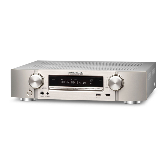
NR1504
Copyright 2013 D&M Holdings Inc. All rights reserved.
WARNING: Violators will be prosecuted to the maximum extent possible.
NR1504 /
U1B/N1B/N1SG
AV Surround Receiver
/K1B
Ver. 3
Please refer to the
MODIFICATION NOTICE.
Advertisement
Table of Contents

Related Manuals for Marantz NR1504 /U1B


Summary of Contents for Marantz NR1504 /U1B
- Page 1 Service NR1504 / U1B/N1B/N1SG /K1B Manual AV Surround Receiver • For purposes of improvement, specifications and design are subject to change without notice. • Please use this service manual with referring to the operating instructions without fail. • Some illustrations using in this service manual are slightly different from the actual set. Ver.
-
Page 2: Table Of Contents
CONTENTS ABOUT THIS MANUAL .............4 LEVEL DIAGRAM ..............89 What you can do with this manual ..........4 Using Adobe Reader (Windows version) ........5 BLOCK DIAGRAM ..............95 SAFETY PRECAUTIONS ............7 POWER DIAGRAM ..............96 NOTE FOR SCHEMATIC DIAGRAM .........8 WIRING DIAGRAM ..............97 NOTE FOR PARTS LIST ............8 PRINTED WIRING BOARDS ...........98 TECHNICAL SPECIFICATIONS ..........10 SCHEMATIC DIAGRAMS (1/25) ...........107... - Page 3 MARANTZ DESIGN AND SERVICE Using superior design and selected high grade components, MARANTZ company has created the ultimate in stereo sound. Only original MARANTZ parts can insure that your MARANTZ product will continue to perform to the specifications for which it is famous.
-
Page 4: About This Manual
ABOUT THIS MANUAL Read the following information before using the service manual. What you can do with this manual Search for a Ref. No. (phrase) Jump to the target of a schematic diagram connector (Ctrl+Shift+F) You can use the search function in Acrobat Reader to search for a Ref. -
Page 5: Using Adobe Reader (Windows Version)
Using Adobe Reader (Windows version) Add notes to this data (Sign) Magnify schematic / printed wiring board diagrams - 1 The Sign function lets you add notes to the data in (Ctrl+Space, mouse operation) this manual. Save the file once you have finished adding notes. Press Ctrl+Space on the keyboard and drag the [Example using Adobe Reader X] mouse to select the area you want to view. - Page 6 Magnify schematic / printed wiring Magnify schematic / printed wiring board diagrams - 2 board diagrams - 3 (Pan & Zoom function) (Loupe Tool function) The Pan & Zoom function lets you see which part of The Loupe Tool function lets you magnify a specific a magnified diagram is being shown in a separate part of a diagram in a separate window.
-
Page 7: Safety Precautions
SAFETY PRECAUTIONS The following items should be checked for continued protection of the customer and the service technician. leakage current check Before returning the set to the customer, be sure to carry out either (1) a leakage current check or (2) a line to chassis resistance check. -
Page 8: Note For Schematic Diagram
NOTE FOR SCHEMATIC DIAGRAM WARNING: Parts indicated by the z mark have critical characteristics. Use ONLY replacement parts recommended by the manufacturer. CAUTION: Before returning the set to the customer, be sure to carry out either (1) a leakage current check or (2) a line to chassis resistance check. If the leakage current exceeds 0.5 milliamps, or if the resistance from chassis to either side of the power cord is less than 460 kohms, the set is defective. - Page 9 Personal notes:...
-
Page 10: Technical Specifications
TECHNICAL SPECIFICATIONS n Audio section n Tuner section • Power amplifier (Note: μV at 75 Ω/ohms, 0 dBf = 1 x 10–15 W) Receiving Range: FM 87.5 MHz – 107.9 MHz Rated output: AM 520 kHz – 1710 kHz Front: Usable Sensitivity: FM 1.2 μV (12.8 dBf) 50 W + 50 W (8 Ω/ohms, 20 Hz –... -
Page 11: Caution In Servicing
PRESET CH PRESET CH Service Jig When you repair the printing board, you can use the following JIG (Extension cable kit). Please order it from Marantz Official Service Distributor in your region if necessary. 8U-110084S EXTENSION UNIT KIT 1 Set... -
Page 12: Disassembly
DISASSEMBLY • Disassemble in order of the arrow in the following figure. • In the case of the re-assembling, assemble it in order of the reverse of the following flow. • In the case of the re-assembling, observe "attention of assembling". •... -
Page 13: Front Panel Assy
About the photos used for "descriptions of the DISASSEMBLY" section • The shooting direction of each photograph used herein is indicated on the left side of the respective photograph as "Shooting direction: ***". • Refer to the diagram below about the shooting direction of each photograph. •... - Page 14 (2) Disconnect the connector wires and FFC. Remove the Style pin and screws. CP4401 Remove:ACETA TAPE STYLE PIN:Loosen STYLE PIN : Loosen N2801 (3) Remove the screws and Style pin. Shooting direction: C Shooting direction: D STYLE PIN : Loosen Please refer to "EXPLODED VIEW"...
-
Page 15: Radiator Assy
2. RADIATOR ASSY Proceeding : TOP COVER → RADIATOR ASSY (1) Remove the screws. View from the bottom (2) Remove the screws and Style pin. STYLE PIN : Loosen Shooting direction: C Shooting direction: D... - Page 16 (3) Disconnect the connector wires and FFC. Remove the Style pin and screws. (4) Disconnect the connector wires. STYLE PIN : Loosen CP4802 CP4800 CP4801 Please refer to "EXPLODED VIEW" for the disassembly method of each PCB included in RADIATOR ASSY.
-
Page 17: Reg Assy
3. REG ASSY Proceeding : TOP COVER → RADIATOR ASSY → REG ASSY (1) Disconnect the connector wires, then remove the screws. CP4602 CP4603 CP4615 CP4614 Shooting direction: B Please refer to "EXPLODED VIEW" for the disassembly method of each PCB included in REG ASSY. -
Page 18: Pcb Rc5_Mx
4. PCB RC5_MX Proceeding : TOP COVER → PCB RC5_MX (1) Remove the screws. Shooting of photograph: A (2) Disconnect the connector board. Board to board... -
Page 19: Pcb Hdmi Assy
5. PCB HDMI ASSY Proceeding : TOP COVER → → PCB RC5_MX PCB HDMI ASSY (1) Disconnect the connector wires and FFC, then disconnect the connector board. STYLE PIN : Loosen N3405 CX1000 N2801 Board to board NOTE : When you remove a HDMI board, be careful of breakage of "PCB FRONT_CNT". -
Page 20: Power Trans Main
6. POWER TRANS MAIN Proceeding : TOP COVER → → PCB HDMI ASSY → POWER TRANS MAIN PCB RC5_MX (1) Cut the wire clamp band, then disconnect the connector wires and Style pin. CP4001 STYLE PIN : Loosen CP4142 (2) Disconnect the connector wires. CP4602 CP4603 Shooting direction: B... - Page 21 (3) Remove the Style pin. Shooting direction: D CP4401 STYLE PIN : Loosen (4) Remove the screws. View from the bottom NOTE : It will separate and TRANS will fall from SET, if screws is removed.
-
Page 22: Av Assy
7. AV ASSY Proceeding : TOP COVER → → PCB HDMI ASSY → PCB RC5_MX AV ASSY (1) Disconnect the connector wires, then remove the screws. CP4401 CP4401 CN4002 Please refer to "EXPLODED VIEW" for the disassembly method of each PCB included in AV ASSY. 8. -
Page 23: Pcb Spk
9. PCB SPK Proceeding : TOP COVER → → PCB HDMI ASSY → PCB RC5_MX AV ASSY → → PCB SMPS PCB SPK (1) Remove the screws. View from the bottom (2) Disconnect the connector wires, then remove the screws and Style pin. Remove the screws, after remove the RADIATOR ASSY. -
Page 24: Special Mode
SPECIAL MODE Special mode setting button No.1-6,10,13: Press the "ON/STANDBY ( X )" button to turn on the power while pressing both the button A and the button B at the same time. No.7-9,11: Turn on the power, then press and hold down the A and B buttons for over 3 seconds. No.12: Turn on the power, then press and hold down the A and B buttons for over 10 seconds. -
Page 25: Μcom/Dsp Version Display Mode
1. µcom/DSP Version display mode 1.1. Operation specifications µcom/DSP version display mode: When the set is started up in this mode, the version information is displayed. Starting up: Press the "ON/STANDBY ( X )" button to turn on the power while pressing the "DISPLAY" and "STATUS" buttons. Now, press the "STATUS"... - Page 26 i Ethernet(DM860A) 1st Boot Loader, Hardware ID : E t h e r n e t F B L Press the "STATUS" button. * * * * * * - b d o Ethernet(DM860A) 2nd Boot Loader, Rhapsody Flag : E t h e r n e t S B L Press the "STATUS"...
- Page 27 1.3. Error display See the following table for each "Error information" display and its explanation (status). Display order is q , w , e , r . Condition Status FL Display Trouble shooting • Please check the Compared with the destination setting destination-resistors on the board.
- Page 28 1.4. Version display on the Setup Menu Use the following procedure to display the firmware version. (1) Press the “SETUP” button on the remote control. (2) Select “General-Information-Firmware”. A version with 12 digits is displayed as shown in the following image. Firmware Version 8200-2593-2131...
-
Page 29: Panel/Remote Lock Selection Mode
2. PANEL/REMOTE LOCK Selection mode 2.1. Behavior specifications In this mode, you can switch between the PANEL LOCK MODE and the Mode for preventing remote control acceptance. 2.2. Starting up Press the "ON/STANDBY ( X )" button to turn on power while pressing the "DISPLAY" and "M-DAX" buttons. Press the "PRESET CH +"... -
Page 30: Service Related Selection Mode
3. Service Related Selection mode 3.1. Behavior specifications In this mode, you can switch between the Diagnostic mode (SERVICE CHECK) and the Displaying the protection mode (PROTECTION). 3.2. Starting up Press the "ON/STANDBY ( X )" button to turn on power while pressing the "PRESET CH-" and "STATUS" buttons. Press the "PRESET CH+"... - Page 31 3.4. DIAGNOSTIC MODE (Video/Audio (signal) path confirmation mode 3.4.1. Specification This mode is used for confirming the Video and Audio (signal) paths. (Troubleshooting) Confirming the operation of unit can be easily done after repair. Backup data will not be lost. 3.4.2.
- Page 32 3.4.6 Audio system confirmation items fig. XX: Refer to the block diagram of the fig.XXth. Confirmation item FL display settings Contents of confirmationRemarks analog pass Input Source: CBL/SAT ·Analog input ⇒ Speaker output A 0 1 : A N A L O G P A S S fig.7 Input Mode: ANALOG(fixed)
-
Page 33: Block Diagram
BLOCK DIAGRAM NR1504 VIDEO DIAGRAM Fig.1:Analog Video (Signal) Pass SPI FLASH HDMI IN HDMI1 HDMI2 TMDS IN TMDS SW ADV3002 HDMI3 HDMI OUT HDMI4 ADV7623 TMDS OUTPUT OUT1 HDMI TRANSCEIVER TMDS IN HDMI5 ADV8195 TMDS IN FRONT HDMI BUFFER TMDS IN USBD+/- CCIR-656(8-BIT) DM860A... - Page 34 NR1504 VIDEO DIAGRAM Fig.2:HDMI Pass (Main) SPI FLASH HDMI IN HDMI1 HDMI2 TMDS IN TMDS SW ADV3002 HDMI3 HDMI OUT HDMI4 ADV7623 TMDS OUTPUT OUT1 HDMI TRANSCEIVER TMDS IN HDMI5 ADV8195 TMDS IN FRONT HDMI BUFFER TMDS IN USBD+/- CCIR-656(8-BIT) DM860A SLI11131 ETHERNET...
- Page 35 NR1504 VIDEO DIAGRAM Fig.3:HDMI CEC SPI FLASH HDMI IN HDMI1 HDMI2 TMDS IN TMDS SW ADV3002 HDMI3 HDMI OUT HDMI4 ADV7623 TMDS OUTPUT OUT1 HDMI TRANSCEIVER TMDS IN HDMI5 u COM ADV8195 TMDS IN FRONT HDMI BUFFER TMDS IN USBD+/- CCIR-656(8-BIT) DM860A SLI11131...
- Page 36 NR1504 AUDIO DIAGRAM fFg.4:HDMI Audio(AVR) 28.6363MHz 28.6363MHz HDMI IN HDMI IN ADV 7623 HDMI1 HDMI1 HDMI TRANCEIVER TMDS HDMI2 HDMI2 HDMI TMDS HDMI OUT1 HDMI OUT1 ARC_+/- SWITCHER AUDIO ARC_+/- ARC_+/- HDMI3 HDMI3 RXI2S ADV3002 PROCESSOR RXMCLK HDMI4 HDMI4 RX64FS RXFS HDMI5 HDMI5...
- Page 37 NR1504 AUDIO DIAGRAM Fig.5:HDMI Audio(Audio : TV) 28.6363MHz HDMI IN ADV 7623 HDMI1 HDMI TRANCEIVER TMDS HDMI2 HDMI TMDS HDMI OUT1 ARC_+/- SWITCHER AUDIO ARC_+/- RXI2S HDMI3 ADV3002 PROCESSOR RXMCLK HDMI4 RX64FS RXFS HDMI5 HDMI RECEIVER DATAF_ADV PROCESSOR DSPOUTFS_ADV DSPOUT64FS_ADV ADV8195 FRONT ARCSPDIF...
- Page 38 NR1504 VIDEO DIAGRAM Fig.6:GUI menu SPI FLASH HDMI IN HDMI1 HDMI2 TMDS IN TMDS SW ADV3002 HDMI3 HDMI OUT HDMI4 ADV7623 TMDS OUTPUT OUT1 HDMI TRANSCEIVER TMDS IN HDMI5 u COM ADV8195 TMDS IN FRONT HDMI BUFFER TMDS IN USBD+/- CCIR-656(8-BIT) DM860A SLI11131...
- Page 39 NR1504 AUDIO DIAGRAM Fg.7:Analog (Signal) Pass 28.6363MHz 28.6363MHz HDMI IN ADV 7623 HDMI1 HDMI TRANCEIVER TMDS HDMI2 HDMI TMDS HDMI OUT1 ARC_+/- SWITCHER AUDIO ARC_+/- ARC_+/- RXI2S HDMI3 ADV3002 PROCESSOR RXMCLK HDMI4 RX64FS RXFS HDMI5 HDMI RECEIVER DATAF_ADV PROCESSOR DSPOUTFS_ADV DSPOUT64FS_ADV ADV8195 FRONT...
- Page 40 NR1504 AUDIO DIAGRAM Fig.8:DIGITAL 28.6363MHz 28.6363MHz HDMI IN ADV 7623 HDMI1 HDMI TRANCEIVER TMDS HDMI2 HDMI TMDS HDMI OUT1 ARC_+/- SWITCHER AUDIO ARC_+/- ARC_+/- HDMI3 RXI2S ADV3002 PROCESSOR RXMCLK HDMI4 RX64FS RXFS HDMI5 HDMI RECEIVER DATAF_ADV PROCESSOR DSPOUTFS_ADV DSPOUT64FS_ADV ADV8195 FRONT ARCSPDIF TMDS...
- Page 41 NR1504 AUDIO DIAGRAM Fig.9:HDMI 28.6363MHz 28.6363MHz HDMI IN ADV 7623 HDMI1 HDMI TRANCEIVER TMDS HDMI2 HDMI TMDS HDMI OUT1 ARC_+/- SWITCHER AUDIO ARC_+/- ARC_+/- RXI2S HDMI3 ADV3002 PROCESSOR RXMCLK HDMI4 RX64FS RXFS HDMI5 HDMI RECEIVER DATAF_ADV PROCESSOR DSPOUTFS_ADV DSPOUT64FS_ADV ADV8195 FRONT ARCSPDIF TMDS...
- Page 42 NR1504 AUDIO DIAGRAM Fig.10:Analog A/D 28.6363MHz 28.6363MHz HDMI IN ADV 7623 HDMI1 HDMI TRANCEIVER TMDS HDMI2 HDMI TMDS HDMI OUT1 ARC_+/- SWITCHER AUDIO ARC_+/- ARC_+/- HDMI3 RXI2S ADV3002 PROCESSOR RXMCLK HDMI4 RX64FS RXFS HDMI5 HDMI RECEIVER DATAF_ADV PROCESSOR DSPOUTFS_ADV DSPOUT64FS_ADV ADV8195 FRONT ARCSPDIF...
- Page 43 3.5. Errors checking mode (Displaying the protection history) 3.5.1.Operation specifications Error mode (Displaying the protection history): When the set is started up in this mode, the error information is displayed. 3.5.2.About the display on the FL display When the "STATUS" button is pressed after the error (protection history display) mode is set, a history like the one shown below is displayed, depending on the conditions.
-
Page 44: Specifications
3.5.3.Clearing the protection history There are two ways to clear the protection history, as described below. (1) Start up the set in error (protection display) mode and display the error, then press and hold down the "DISPLAY" button for 3 seconds. P R T : D C Press and hold down "DISPLAY"... -
Page 45: Dual Backup Memory
4. DUAL BACKUP MEMORY This product has a Dual Backup Memory function. The conventional Backup functions to memorize, in the EEPROM ("IC1024") in the circuit, a current setting of the moment the main power is turned off so that it can be restored when it is turned ON again. -
Page 46: Protection Pass Mode
5. Protection Pass mode 5.1. Specifications • Turn the power on with Protection disabled. Except for disabling the Protection detection, this operation is the same as the normal power on. 5.2. Operation Press the "Power Operation ( X )" button while pressing "DISPLAY"... -
Page 47: Network Initialization Mode
7. NETWORK Initialization mode 7.1. Behavior specifications Initializes NETWORK related settings. (1) Favorites (2) Favorites Station (3) Presets (4) Internet Radio Recently Played (5) Flickr contacts (6) User ID (7) Resume Playback station 7.2. Starting up q Turn on the power and switch to NETWORK FUNCTION. w Wait until ”No Network Connection”... -
Page 48: Jig For Servicing
When you repair the printing board, you can use the following JIG (Extension cable kit). Please order it from Marantz Official Service. Distributor in your region if necessary. NOTE: The incorrect connection with in the JIG (EXTENSION UNIT KIT) may cause damage. - Page 49 Board to board PCB VIDEO (3) Detach PCB HDMI from the chassis, and turn it over. Please put an insulation sheet that is larger than PCB HDMI under PCB. Attach the BACK PANEL. PCB HDMI Insulation sheet Board to board b Connect the ground point of PCB to the chassis with a ground lead or the like.
-
Page 50: When The Microprocessor Is Replaced With A New One
WHEN THE MICROPROCESSOR IS REPLACED WITH A NEW ONE When the U-PRO (Microprocessor) or the Flash ROM is replaced, confirm the following. After PCB Name Ref. No. Description Remark replaced HDMI IC1023 R5F56108VNFP SOFTWARE: Main HDMI U1006 EN29LV160DBTI SOFTWARE: DSP ROM HDMI IC1012 EPM3032A-TC44 SOFTWARE: AUDIO PLD... - Page 51 [All model commonness] 1.3. Turn on the AV receiver Operate the following. Turn on the AV receiver. (1) Connect the power cable to the AC outlet while simultaneously pushing the "M-DAX" and "SOUND MODE" button of the front panel. (2) Confirm the power indicator is green and "WRITTING" is displayed in the front panel. 1.4.
- Page 52 (3) When connection is good, then you can see the "Communication check OK." message. (4) If connection is not good, then you can see the "Communication check NG" message. Please confirm the following (a) Check the connection of the AV receiver and PC. (refer to "1.2. Connection of the AV receiver" ) (b) Check the operation mode of the AV receiver.
- Page 53 1.7. Complete the firmware updating (1) Click the "Update" button. XXXXXXXX XXXXXXX (2) When writing of the firmware is completed, the power of AV receiver turns on automatically and you can see the "Update completed" message. When U2603 is replaced, update the firmware and then run “Network Initialization mode”.(47 page) (3) If you can’t complete the firmware update, please retry the firmware update from "1.3.
-
Page 54: How To Update By Dpms
2. How to update by DPMS You can update the firmware by downloading the latest version from the Internet. 2.1. Connecting to the Network (1) System requirements • Internet Connection by Broadband Circuit • Modem • Router • Ethernet cable (CAT-5 or greater recommended) (2) Setting Internet Computer... - Page 55 2.3. About the error code See the table below for error codes, details of faults, and coping strategies when the firmware is updated through DPMS (Marantz Product Management Server). Error Details of Error code Display Coping strategies Code Reset and update again.
- Page 56 Error Details of Error code Display Coping strategies Code Main CPU failed to receive firmware Turn off and on the power. for rewriting sent from DM860A (when U p d a t i n g f a i l Updating starts automatically. an error occurred).
- Page 57 Error Details of Error code Display Coping strategies Code Check the network connection. Connection to DPMS timed out Carry out the update in an environment C o n n e c t i o n F a i l 3 9 when Main CPU was rewritten.
- Page 58 Error Details of Error code Display Coping strategies Code DSP, PLD etc. failed to receive Turn off and on the power. firmware for rewriting sent from U p d a t i n g f a i l Updating starts automatically. DM860A (when timed out).
- Page 59 Error Details of Error code Display Coping strategies Code Line congestion via DPMS access Check the network connection. was notified when DM860A related Carry out the update in an environment S e r v e r b u s y A 3 firmware was rewritten (Application that has little network load.
- Page 60 Device display during firmware update Display of target device during firmware update. Target device Display Error code when an error occurs 08 - 0C 10 - 15 Main M a i n : * * % * * * m i n 22 - 24 36 - 3E 50 - 52...
-
Page 61: How To Update By Usb Memory
3. How to update by USB Memory You can update the firmware by downloading the latest version with USB Memory. 3.1. Connecting to the USB (1) Requirements • The USB memory device format should be set to FAT16 or FAT32. •... - Page 62 USB location is below USB memory root Model Name Model Area Product ID NR1504 U1 North America (E3) 100100190100 NR1504 N1 Europe (E2) / Singapore(E1) 100100190200 NR1504 K1 China (E1C) 100100190500 + firmwares + 100100190100 + APLD.bin + DSP.bin + enc_update.xml + GUI.bin + IMG.bcd + MAIN.bin...
- Page 63 3.5. Start update Turn on the power of this unit in the "DISPLAY" + "SOUND MODE" button. 3.6. "USB Update Start" on FL Display After arround half minutes, FL display shows the following message. FL Display Upper * F I R M W A R E U P D A T E Lower U S B...
- Page 64 3.3. About the error code See the table below for error codes and details of faults when the firmware is updated through USB memory. Error Details of Error code Display Coping strategies Code Disconnect and connect the USB Unable to detect USB. C o n n e c t i o n F a i l 0 1 memory.
- Page 65 Error Details of Error code Display Coping strategies Code No FirmwareFile in USB after Disconnect and connect the USB F i l e s N o t F o u n d SBLMode. memory. FirmwareFile in USB after SBLMode Check the supported Model name/area N o t M a t c h F i r m for unsupported Model name/area for the FirmwareFile.
- Page 66 Error Details of Error code Display Coping strategies Code This unit automatically retries several times. Wait until the FL display stops. No FirmwareFile in USB. If the FL display stops at the Error F i l e s N o t F o u n d display, press and hold the "ON/ STANDBY ( X )"...
- Page 67 Error Details of Error code Display Coping strategies Code This unit automatically retries several Mismatched CheckSum in response times. Wait until the FL display stops. or no response from Sub for I If the FL display stops at the Error U p d a t e C h e c k N G command.
- Page 68 Error Details of Error code Display Coping strategies Code This unit automatically retries several times. Wait until the FL display stops. FirmwareFile in USB for unsupported If the FL display stops at the Error N o t M a t c h F i r m Model name/area display, press and hold the "ON/ STANDBY ( X )"...
- Page 69 3.4. Device display during firmware update Display of target device during firmware update. Target device Display Error code when an error occurs 08 - 0B 10 - 15 Main CPU 20 - 27 M a i n : * * % * * * m i n 36 - 3B 50 - 52...
-
Page 70: Adjustment
ADJUSTMENT Audio Section Adjusting Idling Current Required measurement equipment: DC Voltmeter 1. Preparation (1) Temperature should be at avoid direct blow from an air conditioner or an electric fan and humidity should be moderate, and place the set at normal usage environment. 15 °C ~ 30 °C (59 °F ~ 86 °F) (2) Presetting •... -
Page 75: Trouble Shooting
TROUBLE SHOOTING 1. POWER 1.1. Power not turn on Power not turn on. When the power turned on, When the power turned on, does the ON/STANDBY does the ON/STANDBY indicator on the front panel indicator on the front panel flashing green? flashing red? Refer to 1.2.Fuse is blown. -
Page 76: Analog Video
2. Analog video MONITOR OUT (CVBS/HDMI) output NG Input CVBS/ Input SOURCE : CBL/SAT HDMI To troubleshooting To A 3.2 HDMI/DVI. - Page 77 Output CVBS Check on set value of each IC. Is they the following voltage values? HDMI B'D HDMI B'D flaw. N3404-4pin : L(0V) N3404-5pin : H(5V) Extend HDMI B'D using a jig. Is the power supply voltage correctly output? Check connection of FRONT V+5V : C5407 : + side CONNECTOR BD and AV BD.
- Page 78 HDMI test point BAR CODE HDMI PCB CX1000 N3404 N3402 7028-07387-101-0 C1113 FB1015 C1116 C1482 C1484 CLP1001 C1471 C1048 C1497 R1315 FB1013 C1453 R1316 CP1001 C1077 R1271 R1273 C1518 U1003 N3403 C1091 C1120 C1511 C1505 C1455 N3405 R1376 C1103 C1227 C1228 C1341 C1114 IC1017...
-
Page 79: Hdmi/Dvi
(6) Is the BD/DVD player's HDMI output setting correct? the BD/DVD player's operating instructions. (7) When you use a Marantz BD/DVD player's, is the fluorescent display tube's "HDMI" indicator lit? If you use a non-Marantz BD/ DVD player's, proceed to "YES". - Page 80 Check TV Use an HDCP-compatible TV. PC TVs (11) Is the TV HDCP-compatible? cannot be used. If the TV is not compatible with resolutions of 1080P, no picture will be output, even (12) Is the TV compatible with resolutions of 1080P? if the BD/DVD player's resolution is set to 1080P.
-
Page 81: Audio
4. AUDIO 4.1. AUDIO CHECK Audio output NG. CHECK1 INPUT SURROND MODE SOURCE Check ANALOG audio BLOCK. Audio output OK? ANALOG 2CH DIRECT ANALOG CHECK2 INPUT SURROND MODE SOURCE Check Digital audio BLOCK. Legacy Audio output OK? COAX or OPT Don't care (PCM or DolbyDigital or dts…) CHECK3... - Page 82 4.2. Power AMP (MAIN UNIT) No sound is output. The protector operates. Is the power transistor open or short- circuited? Replace the power transistor. 2SB1560/2SD2390 Is the emitter resistance of the power transistor open? Replace the emitter resistance. 0.47Ω Is the base resistance of the power transistor open? Replace the base resistance.
-
Page 83: Analog Audio
4.3. Analog audio No sound is output Is the voltage of ±7V supplied to The power supply of ±7V is repaired. AV B'D CP5201? Is the audio signal transmitted to The power amplifier is repaired. AV B'D CP5202? Connect the connectors properly. Is the serial data for electronic volume Is the connector correctly connected transmitted to AV B'D CP5200? -
Page 84: Network/Usb
5. Network/USB 5.1. Cannot connect to network Checking the environment Turn off the power and check the LAN cable Is the LAN cable properly connected? properly, and then turn the power back on. Checking the settings Set the IP address and other parameters properly. - Page 85 5.2. USB device is not recognized Checking the USB device Are you using a USB hub? Don't use the USB hub. Only mass storage devices in FAT16 or FAT32 format or MTPcompatible devices Is the USB device compatible with the set? and iPod (Remove some models) are supported.
- Page 86 HDMI test point BAR CODE HDMI PCB CX1000 N3404 N3402 7028-07387-101-0 C1113 FB1015 C1116 C1482 CX1000 C1484 CLP1001 C1471 C1048 C1497 R1315 FB1013 C1453 R1316 CP1001 C1077 R1271 R1273 C1518 U1003 N3403 C1455 N3405 C1091 C1120 C1511 C1505 R1376 C1103 C1341 C1227 C1228 C1114...
-
Page 87: Smps
6. SMPS DC 5V is not output. Is there damage in IC4140 Replace the IC4140 (TOP258MG) and (TOP258MG)? D4142/D4143/D4144/D4145. Is there the damage in D4142/D4143/ Is the fuse (F4140) blown? Replace the damaged parts. D4144/D4145/IC4140? Is there solder short circuit in the PCB Repair the solder short part of the PCB board? board. - Page 88 Operation waveform for each part Primary drain (Caution: High voltage, electric shock) After primary side rectification (Caution: High voltage, electric shock) After secondary rectifications OPTION L4141 C4148 0.01/250V OPTION OPTION L4140 F4140 SQ2014 LIVE JP4140 JUMPER D4142 1N4007 JK4140 ZD4151 AC INLET D4143 1N4007...
-
Page 89: Level Diagram
LEVEL DIAGRAM LEVEL DIAGRAM FRONT ch R2A15218FP ANALOG H/POUT + SPEAKER LINE IN GAIN + PCM1690 + PCM9211 + - - MUTE PRE OUT ZONE2 EXT IN (SR5008,NR1604 ONLY) (SR5008 ONLY) +30dB SP OUT 4.48Vrms/8Ω MAX SIGNAL LEVEL 0dBFS +20dB +20dB 1.41Vrms PCM1690... - Page 90 LEVEL DIAGRAM CENTER ch R2A15218FP + SPEAKER GAIN PCM1690 (SR5008 ONLY) + + - - MUTE PRE OUT EXT IN (SR5008 ONLY) +30dB SP OUT 4.48Vrms/8Ω 0dBFS MAX SIGNAL LEVEL 1.41Vrms +20dB +20dB DOLBY LIMIT LEVEL (ALLch-3dBFS) 0dBFS +29dB +10dB +10dB -10dBFS -20dBFS(DIG.IN)
- Page 91 LEVEL DIAGRAM SUBWOOFER ch R2A15218FP MUTE PRE OUT GAIN PCM1690 + + SW2 (SR5008 ONLY) - - MUTE PRE OUT EXT IN (SR5008 ONLY) +30dB MAX SIGNAL LEVEL Config1 DOLBY LIMIT LEVEL (ALLch-3dBFS) 0dBFS 0.88Vrms +20dB +20dB 0dBFS +10dB +10dB -10dBFS PREOUT 317mVrms...
- Page 92 LEVEL DIAGRAM SURROUND ch R2A15218FP + SPEAKER GAIN PCM1690 (SR5008 ONLY) + + - - MUTE PRE OUT EXT IN (SR5006 ONLY) +30dB SP OUT MAX SIGNAL LEVE 4.48Vrms/8Ω 0dBFS 1.41Vrms +20dB +20dB 0dBFS Config2 DOLBY LIMIT LEVEL 1.41Vrms(ALLch-3dBFS) +29dB +10dB +10dB -10dBFS...
- Page 93 LEVEL DIAGRAM SURR.BACK ch R2A15218FP + SPEAKER GAIN PCM1690 + (SR5008 ONLY) + - - MUTE PRE OUT EXT IN (SR5008 ONLY) +30dB SP OUT NON CLICP MAX SIGNAL LEVEL 4.0Vrms 4.48Vrms/8Ω SP OUT(D/A OUT) 0dBFS DOLBY LIMIT LEVEL 1.41Vrms(ALLch-3dBFS) 1.41Vrms +20dB +20dB...
- Page 94 LEVEL DIAGRAM ZONE2 R2A15218FP from F-ch from SPEAKER DA SB-ch + LINE IN + MAIN NET/USB DAC BD3812F ZONE2 +30dB SP OUT 0dBFS PCM5100 2.0Vrms MAX SIGNAL LEVEL 2.00Vrms +20dB +20dB 0dBFS -10dBFS +10dB +10dB -20dBFS(DIG.IN) LINE IN 200mV -20dBFS PREOUT -18.0dB 16.0dB...
-
Page 95: Block Diagram
BLOCK DIAGRAM NR1504 GND BLOCK DIAGRAM AC CORD HDMI B'D A_GND RET_GND MAIN + SPK B'D D_GND D_GND A_GND D_GND MAIN TRANS VOL_IC FRONT_CNT B'D SMPS_S3 V_GND V_GND A_GND A_GND JUMPER SHORT REG_CNT B'D RET_GND AUDIO S2 VIDEO S4 A_GND V_GND SMPS B`D AMP +B S1... -
Page 96: Power Diagram
POWER DIAGRAM NR1504 VCC DIAGRAM MAIN +B S1(AMP +B) MAIN -B NJM7808FA A+8.0V (Pre) S2(+8V,-8V) DA+5.0V NJM7805FA A-8.0V (Pre) NJM7908FA MAIN TRANS S4(VIDEO) A.V+5.0V NJM7805FA A.TUNER+5.0V RELAY A.V-5.0V NJM7905FA -VKK S5(VKK) FL AC (F1) S6(FILAMENT) FL AC (F2) D5V(MX-PORT) M3.3V (CPU) NJM2845DL1 AC CORD SWM3.3V (FLT) -
Page 97: Wiring Diagram
WIRING DIAGRAM NR1504 WIRING BLOCK DIAGRAM AC CORD MAIN + SPK B'D HDMI + USB B'D RC5/M-X B'D FRONT CNT B'D MAIN POWER TRANS VIDEO+INPUT B'D REG-CNT B'D S3 TAP S2 TAP SMPS B'D 7808 7908 7805 7905 7805 D10SB60 5CH AMP B'D 23P CARD CABLE FRONT B'D... -
Page 98: Printed Wiring Boards
PRINTED WIRING BOARDS Lead-free Solder When soldering, use the Lead-free Solder (Sn-Ag-Cu). HDMI (A SIDE) FRONT HDMI (A SIDE) BAR CODE HDMI PCB CX1000 N3404 N3402 7028-07387-101-0 C1113 FB1015 N1005 C1116 C1482 CLP1001 C1484 C1471 C1048 C1497 R1315 FB1013 R1051 R1057 C1453 R1053... - Page 99 FRONT HDMI (A SIDE) HDMI (A SIDE) C1485 R1333 R1360 C1165 R1321 C1500R1322 R1552 FB1014 C1477 C1495 C1502 R1359 C1180 C1080 R1243 C1166 FB1012 C1183 C1585 C1487 C1185 C1182 C1167 C1184 C1179 C1472 R1379 C1508C1514 C1206 C1204 IC1016 C1215 C1220 NJM8080G C1216 C1068...
- Page 100 GUIDE-L (A SIDE) HDMI-GUIDE-B (A SIDE) SPK (A SIDE) C4025 JACK4000 J4025 J4033 C4027 C4029 C4028 C4026 J4042 C4024 J4019 R4007 C4001 C4023 J4058 J4041 L4001 RLY4001 L4003 J4028 J4057 C4011 C4009 R4008 R4009 R4001 R4010 C4003 C4008 RLY4000 J4024 L4002 R4000 J4032...
- Page 101 GUIDE-L (B SIDE) HDMI-GUIDE-B (B SIDE) SPK (B SIDE) C4047 C4043 C4052 C4035 C4040 C4046 C4034 C4051 C4048 C4045 C4042 C4036 C4033 C4039 C4044 C4041 C4050 C4049 C4037 C4032 C4038 HDMI_GUIDE_B C4018 7028-07389-701-0 C4019 C4021 C4020 C4022 C4016 C4017 D4000 SPK B'D Q4003 LIMIT-...
- Page 102 AV (A SIDE) AV (B SIDE) R5423 R5425 IC5402 C5423 C5419 CN5201 NJM2586AVC3 C5417 R5419 C5424 R5421 C5422 R5415 R5417 CN5401 C125Z2-13 1.D/MGND NR1604 AV PCB(MP) C5418 1.D/MGND 2.NC 2.NC 3.D/MGND NR1604 AV PCB(MP) 3.D/MGND 4.NC 7020-07385-000-0S 4.NC 5.D/MGND 5.D/MGND 7020-07385-000-0S 6.CVBS C5420...
- Page 103 FRONT (A SIDE) C4406 BAR CODE J4073 ZD4400 J4029 FIL2 R4402 C4407 OPEN VEC4400 C4404 C4429 CP4400 SOURCE SEL VEC4401 FIL1 J4031 MASTER VOL (CLICK) J4026 (NON CLICK) OPEN D4401 J4049 J4059 J4011 OPEN J4067 C4411 RMC4400 C4401 J4025 C4408 -Vkk ZD4402 CP4401...
- Page 104 7CH-AMP (A SIDE) R5091 CP4801 7CH AMP B'D J4888 C4898 TP4802 J4923 C4897 R5092 C4855 7020-07381-000-0S TP4808 VR4803 TP4806 C4884 CLP4800 R5045 VR4802 C4870 +HIGHB C4856 R4998 C4841 TP4804 R4999 +HIGHB R4983 C4869 R5048 C4883 TP4810 CLP4801 C4807 VR4801 +HIGHB C4842 VR4806 R4968...
- Page 105 REG (A SIDE) RC-5_MX (A SIDE) FRONT-CNT (A SIDE) SCREW 3*8 ZD4700 ZJ16B RC-5/M-X B'D 7028-07388-901-0 CP4615 C4703 JP4630 J4661 C4702 CP4612 JP4631 C4636 J4631 CN4606 CN4607 J4672 J4652 C4633 J4674 D4603 J4676 J4670 7.H/P_L C4635 6.H/P_GND J4679 5.H/P_R J4693 4.RLY_F 3.RLY_S/C CLP4606...
- Page 106 FRONT-CNT (B SIDE) RC-5_MX (B SIDE) REG (B SIDE) D4703 RC-5/M-X B'D R4637 IC4700 C4643 PQ120DNA1ZPH R4632 7.H/P_L 6.H/P_GND 5.H/P_R R4631 J4630 4.RLY_F 3.RLY_S/C 2.RLY_SB 1.RLY_H/P R4624 R4625 R4622 Q4601 C4631 R4621 C4645 C4630 C4619 C4626 C4623 R4616 R4620 C4624 R4628 C4618 13.V-5V...
-
Page 107: Schematic Diagrams (1/25)
ADV3002 CEC_COM JACK1001 R1068 R1072 R1076 R1080 AD3PBC19G0-T OPEN HPD/HEAC- DDCDATA Q1004 RT1N141C DDCCLK Q1008 RT1N441C CE_REMOTE CK SHIELD D0 SHIELD D1 SHIELD D2 SHIELD R1115 R1116 OPEN JACK1002 AD3PBC19G0-T R1069 R1073 R1077 R1081 OPEN CEC5V HPD/HEAC- DDCDATA Q1005 RT1N141C DDCCLK Q1009 R1086... -
Page 108: Hdmi_Front-Hdmi
FRONT HDMI R1576 R1577 L1202 0(2012) R1051 R1053 R1055 R1056 OPEN R1052 ZD1008 R1054 OPEN OPEN OPEN N1005 AD3PBJ19G0-REV_B Q1010 RT1N141C HPD/HEAC- Q1011 RT1N441C DDCDATA DDCCLK N1202 1.0-16-23PB-2 CE_REMOTE CEC_COM. CE_REMOTE HP_CTRLA HP_CTRLA CK SHIELD FRONT_HDMI TXEN TXEN DDC_SDA DDCDATA DDC_SCL DDCCLK D0 SHIELD... -
Page 109: Hdmi_Adv7623
ADV7623 CP1001 1.0-16-23PB-2 CE_REMOTE HP_CTRLA. HP_CTRLA TXEN TXEN. DDCDATA DDCA_SDA DDCCLK DDCA_SCL STBY5V FHDMI_5V. FHDMI_5V RESETB CEC5V CEC5V R1118 HPD5V CEC3.3V CEC3.3V CEC3.3V CEC3.3V CEC5V R1119 DGND R1181 OPEN 312mA CEC1.8V DGND R1182 DGND RXA_C- FB1024 L1003 OPEN(2012) BD221T(2012) DV5V RXA_C+ R1200 40mA... -
Page 110: Hdmi_Sli11131A
SLI11131 DGND L1600 BD221T(2012) A3.3VL_PVDD2 L1601 BD221T(2012) A3.3VL_PVDD1 L1602 BD221T(2012) A3.3VL L1603 BD221T(2012) D3.3VL L1604 BD221T(2012) A1.2VL L1605 BD221T(2012) D1.2VL PVDD1 VIDEO C1626 100N-K PVDD1 A3.3VL_PVDD1 C1627 100N-K R1600 PVDD1 A3.3VL_PVDD1 R1601 R1602 PVSS1 R1603 R1604 PVSS1 DGND R1605 PVSS1 DGND AVDD33 R1606... -
Page 111: Hdmi_Dsp
PLD PART CPU PART TO J3 TO J2 DGND DATAC_ADV DSP1OUT64FS_ADV DSP1OUTFS_ADV ADV7623 PART MCLK_ADV TO 6H DATASB_ADV DATAF_ADV DATAS_ADV U1003:10P FFC U1003 1.0-16-10PB-2 DTCK R1311 DATAC_ADV R1312 DTDO DSP1OUT64FS_ADV R1393 R1245 DSP1OUTFS_ADV OPEN DTMS OPEN R1286 TRST DTRST R1396 R1283 OPEN EMU0... -
Page 112: Hdmi_Dir-Pld
DIR/AUDIO PLD TO J5 TO 8H TO J4 TO HDMI RX/TX(ADV7623) TO NET PHY TO CPU *FILTER COMPONENTS VALUE TYPE TOLERANCE 680 Ω ± 5% R2225 METAL FILM OR CARBON ± 5% C2220 0.068UF FILM OR CERAMIC (CH OR C0G) ±... -
Page 113: Hdmi_Main-Dac
MAIN DAC TO J7 TO 6J TO CPU TO DIR/AUDIO PLD R1350 0(1608) R1336 OPEN(1608) R1357 OPEN(1608) C1503 C1517 10/16-MVG OPEN(1608) IC1016:A R1358 4K7(1608) R1325 OPEN OPEN(1608) R1337 OPEN(1608) C1516 OPEN R1333 0(1608) R1334 OPEN(1608) R1359 OPEN(1608) C1518 C1502 IC1016:B 10/16-MVG OPEN(1608) R1360... -
Page 114: Hdmi_Dm860A
DM860A R2709 DM_A18/DQM1 .DM_A18/DQM1 33*4(AR) U2602 DM_A16/BA1 .DM_A16/BA1 DM860A R2714 DM_A15/BA0 .DM_A15/BA0 DM_D3 33*4(AR) JTAG DM_A12 .DM_A12 DM_D2 R2710 R2704 JTAG DM_A10 .DM_A10 33*4(AR) DM_D1 33*4(AR) MP OPEN DM_A14/CAS .DM_A14/CAS ETCK DM_D0 DM_A13/RAS .DM_A13/RAS ETDO USBD- VDD33USB DGND NET3.3V HIGHZ RXD1 DM_A0 DM_A1... -
Page 115: Hdmi_Net-Phy
NET PHY TO 9J TO DM860A TO 5J 860SPDIF DIR/PLD D5V(MX) FROM NET1.2V NET3.3V D.SUPPLY DGND TO K2 E_RESETN NET3.3V NET1.2V R2849 SLI11131A EV_SDA SLI_SDA R2851 EV_SCL SLI_SCL TO 9H R2805 L2806 R2806 DLW21SN181SQ2L N2801 N2801 U2806 20010WS-05 NCP380HMU15AATBG L2804 0(2012) R2864 R2865... -
Page 116: Hdmi_Cpu
TO ADV7623 TO DSP TO DIR/PLD TO CPU LEVEL CHG TO ADV3002 TO K3 TO 7H TO 1H TO 2J TO 4J BDOWN R1515 MAIN_POWER R1516 R1554 0(1608) E_POWER2 E_POWER DA_POWER CEC_POWER D.SUPPLY DV_POWER CPU_POWER D5V_POWER CEC_POWER2 TO K4 1 2 3 4 RESET 94 93 R1449... -
Page 117: Hdmi_Cpu-Level-Chg
CPU LEVEL CHG TO DIGITAL CONNECTOR TO K5 STBY3.3V STBY5V TO K6 SWM3.3V SWM5V(MX) M3.3V DGND FROMD.SUPPLY R1400 CP1002 M3.3V 232MO 232MI SWM3.3V DGND R1398 R1399 DGND OPEN OPEN SWM3.3V 14 13 12 11 10 9 8 14 13 12 11 10 9 8 R1405 R1409... -
Page 118: Hdmi_Digital-Cnt
TO D.SUPPLY/RESET DIGITAL CNT TO K7 DA+5V DA+7V DA-7V NC(USB_L) DAGND NC(USB_R) N3406 DAGND N3406 DAGND C125Z2-07 ADINL A/D_L DAGND TU_SCLK/SCL TU_SCLK/SCL ADINR A/D_R TU_SDIO/SDA TU_SDIO/SDA DAGND TU_SEN TU_SEN DAFL DA_FL SIDE CONNECTOR FROM MAIN DAC TU_RST/ST TU_RST/ST DAGND TU_GPIO2/TUNED TU_GPIO2/TUNED DAFR DA_FR... -
Page 119: Hdmi_D-Supply
D.SUPPLY/RESET FB1012 BD221T(2012) C1018 FB1013 BD221T(2012) 10U-K(2012) FB1014 BD221T(2012) C1009 C1021 10U-K(2012) 10U-K(2012) FB1000 BD221T(2012) FB1010 0(2012) SPK_SMPS B'D 1/2 PVIN VOUT PVIN VOUT D3.3V FB1001 N3601 BD221T(2012) PVIN VOUT 2.08A CX1000 FB1011 R1021 IC1000 TR1005 0(2012) SMW250-5P EX3AV FDC608PZ R1024 D5V_POWER D5.2V... -
Page 120: Spk_Side-Cnt_Spk
SPEAKER B'D JACK4000 R4016 470(1) H/PR FR_GND C4016 C4023 2N2-K FR_A RLY4004 BC3-12 FL_GND C4017 C4024 H/PL 470(1) 2N2-K L4000 SP-2507 R4017 FL_A C4000 R4000 10(2) C_GND 47N(M)-50V C4008 C4018 C4025 47N(M)-50V 2N2-K R4007 10(2) L4001 SP-2507 C4001 R4001 10(2) 47N(M)-50V C4009 RLY4000... -
Page 121: Spk_Side-Cnt_Side-Cnt
SIDE CONNECTOR RC5/M-X PORT REG_CNT 4/4 E5 TO CP4613 TO MX/RC-5 CN4605 CN4605 C125Z2-19 HDMI DIGITAL CNT N3 HDMI DIGITAL CNT G4 TO N3406 TO N3403 CP4604 CP4605 CP4604 CP4605 CP4606 TO HDMI C125Z1-31 C125Z1-07 CP4606 CP4614 CP4614 C125Z1-25 20010WR-11 TRG +15V TRG GND TRG GND... -
Page 122: Av_Input
AV 1/3 SIDE_CNT 2/4 F9 SIDE_CNT 2/4 I9 SIDE_CNT 2/4 D9 TO CN4603 TO CN4602 FRONT_CNT 3/4 J8 REF : 5200-5399 SPK_SMPS 1/2 A9 TO CN4604 TO CP4612 TO CP4000 CP5201 CP5202 CN5200 CP5200 CN5201 CP5201 CP5202 CN5200 CP5200 CN5201 C125Z1-13 C125Z1-23 C125Z2-07... -
Page 123: Av_Video
AV 2/3 REF : 5400-5499 CVBS INPUT SW (MM74HC4051MX) INPUT OUT PUT NR1604 NR1504 A B C L L L MUTE MUTE L H L Blu-ray-DVD L L H CBL/SAT CBL/SAT L H H BLU-RAY MEDIA-PLAYER JK5400_3 MONITOR Y/V. Y/V. R5400 820-D R5401... -
Page 124: Av_Tuner
AV 3/3 REF : 5500-5599 * MODEL/OPTION MODEL NR1604 NR1504 OPTION_B OPEN OPEN OPTION_B R5500 R5501 R5502 TUNER PACK C5500 L5500 OPEN C5501 R5503 OPEN OPEN OPEN R5504 C5502 OPEN PACK5500 R5505 OPEN TUNERL TUNERL TUNERR TUNERR BD5500 BD121T TU_5V TU_5V. -
Page 125: Front_Front
NR FRONT B`D FRONT 1/1 R4403 R4410 REF: 4400-4599 N/K/F 1R2 R4409 - R4400 R4410 0 AUDYSSEY TUNED STEREO SLEEP R4403 0 AUTO HDMI DIGITAL ANALOG S.BACK FIL2 R4401 OPEN MUTE R4404 - FIL1 Q4400 OPEN F4400 KTC1027Y DIG. ANA. Vkk GND 1N4007 1N4007... -
Page 126: Amp_Amp1
7CH_AMP 1/2 REF : 4800-5199 NR AMP B'D 1/2 R4800 R4802 ZD4800 R4801 R4803 R4804 ZJ5.1A 100K 5K6(1) C4800 DHPTHF1608-105T 100N-K C4803 Q4800 C4802 OPEN TP4800 KTA1024Y C4801 R4805 R4809 47/50(6.3*11) 10N-K 680K Q4801 R4806 R4807 R4808 2N5401S 5K6(1) Q4802 100K JUMPER R4813... -
Page 127: Amp_Amp2
PAGE 2 TO G2 PAGE 2 TO G3 AMP B'D 1/2_A10 7CH_AMP 2/2 AMP B'D 1/2_M10 R4934 R4936 R4937 ZD4809 R4935 REF : 4800-5199 ZJ5.1A 100K 5K6(1) R4938 DHPTHF1608-105T C4851 C4849 Q4829 C4850 TP4806 100N-K OPEN KTA1024Y 47/50(6.3*11) R4942 680K Q4830 R4939 R4940... -
Page 128: Smps_Reg_Cnt_Smps
SPK_SMP 1/1 NR SMPS B'D OPTION L4141 C4148 0.01/250V OPTION OPTION L4140 F4140 SQ2014 LIVE JP4140 JUMPER D4142 1N4007 JK4140 ZD4151 AC INLET D4143 1N4007 ZD4147 NEUTRAL 。ワ 。ワ ZJ22B ZJ39B 。ワ 。ワ ZD4152 D4144 1N4007 D4149 ZD4148 ZJ22B ZJ39B SRL3060P D4145 1N4007... -
Page 129: Smps_Reg_Cnt_Reg
REG_CNT 1/4 NR_REG REGULATOR B'D D4608 RB721Q-40 CN4607 CN4607 IC4604 120MM/4P KIA7805API VIDEO+5V VIDEO_+5V FRONT CONNENCTOR VIDEO_GND C4610 VIDEO_GND (REG_CNT 3/4 M7) C4606 D4604 4700/16(16*25) R4600 10/50 1SS133 VIDEO-5V OPEN C4611 R4601 C4607 D4605 3300/16(12.5*25) OPEN 10/50 1SS133 VIDEO_-5V IC4602 KIA7905PI D4610 RB721Q-40... -
Page 130: Smps_Reg_Cnt_Front-Cnt
REG_CNT 3/4 FRONT CONNECTOR HDMI DIGITAL CNT G8 HDMI DIGITAL CNT D6 HDMI DIGITAL CNT C4 TO N3404 TO N3402 CP1008 CP4611 CP1008 CP4607 CP4611 TO HDMI C125Z1-07 C125Z1-13 C125Z1-13 NR1604 ONLY CP4615 CP4615 20010WR-04 VIDEO+5V VIDEO_GND REG_CNT 1/4 B2 VIDEO_GND VIDEO-5V CP4609... -
Page 131: Smps_Reg_Cnt_Rc5
REG_CNT 4/4 NR_RC-5/M-X PORT IC4700 JACK4602 PQ120DNA1ZPH PJ-308-02 (BK) TRIGGER PJ-308-02 ON/OFF D4703 LBAS16HT1G NR1604 ONLY R4618 Q4605 RT1P141C R4619 Q4600 Q4603 RT1P141C RT1N141C C4628 C4629 CP4613 OPEN OPEN 4700N-K CP4613 R4610 C125Z1-19 R4611 OPEN TRG +15V TRG GND TRG1 Q4601 SWM5V(MX) RT1P141C... -
Page 132: Exploded View
EXPLODED VIEW NR1504(Marantz) EXPLODE VIEW WARNING: Parts marked with this symbol z have critical characteristics. Use ONLY replacement parts recommended by the manufacturer. -
Page 133: Parts List Of Exploded View
PARTS LIST OF EXPLODED VIEW Please refer to the last chapter. z Parts for which "nsp" is indicated on this table cannot be supplied. z P.W.B. ASS'Y for which "nsp" is indicated on this table cannot be supplied. When repairing the P.W.B. ASS'Y, check the board parts table and order replacement parts. -
Page 134: Packing View
PACKING VIEW 13 14 UK plug (UK Only) * POLY BAG PACKING STYLE * BOX BOTTOM TAPE( O ) TAPE (CLEAR) S E T CORD AC... -
Page 135: Parts List Of Packing View
PARTS LIST OF PACKING VIEW Please refer to the last chapter. z Parts for which "nsp" is indicated on this table cannot be supplied. z The parts listed below are for maintenance only, might differ from the parts used in the unit in appearances or dimensions. Personal notes:... -
Page 136: Semiconductors
SEMICONDUCTORS Only major semiconductors are shown, general semiconductors etc. are omitted to list. The semiconductor which described a detailed drawing in a schematic diagram are omitted to list. 1. IC's ADV7623 (DIGITAL : IC1007) DDCC_SCL DDCA_SDA CVDD PIN 1 RTERM CGND 5V_DETA RXC_C–... - Page 137 Pin No. Mnemonic Type Description RXC_2− HDMI input Digital Input Channel 2 Complement of Port C in the HDMI Interface. RXC_2+ HDMI input Digital Input Channel 2 True of Port C in the HDMI Interface. HP_CTRLD Digital output Hot Plug Detect for Port D. 5V_DETD Digital input 5 V Detect Pin for Port D in the HDMI Interface.
- Page 138 Pin No. Mnemonic Type Description RXC_2− HDMI input Digital Input Channel 2 Complement of Port C in the HDMI Interface. RXC_2+ HDMI input Digital Input Channel 2 True of Port C in the HDMI Interface. HP_CTRLD Digital output Hot Plug Detect for Port D. 5V_DETD Digital input 5 V Detect Pin for Port D in the HDMI Interface.
- Page 139 Pin No. Mnemonic Type Description PGND Ground PVDD Ground. PVDD Power PLL Supply Voltage (1.8 V). XTAL Miscellaneous Input pin for 28.63636 MHz crystal or an external 1.8 V 28.63636 MHz clock oscillator source to analog clock the ADV7623. XTAL1 Miscellaneous Crystal Output Pin.
- Page 140 ADV7623 Block diagram XTAL XTAL1 VIDEO DATA RXA_C RXB_C RXC_C AUDIO DATA VIDEO DATA RXD_C RXA_0 RXA_1 EQUALIZER SAMPLER RXA_2 AUDIO DATA VIDEO DATA RXB_0 VIDEO DATA EQUALIZER SAMPLER RXB_1 RXB_2 AUDIO DATA RXC_0 SAMPLER AUDIO DATA RXC_1 EQUALIZER RXC_2 RXD_0 EQUALIZER SAMPLER...
- Page 141 www.ti.com SBAS495 – JUNE 2010 PIN CONFIGURATIONS PT PACKAGE PCM9211 (DIGITAL : U2203) LQFP-48 (TOP VIEW) ERROR/INT0 VDDRX NPCM/INT1 RXIN1 MPIO_A0 MPIO_A1 RXIN2 MPIO_A2 RXIN3 MPIO_A3 RXIN4/ASCKIO PCM9211 MPIO_C0 RXIN5/ABCKIO MPIO_C1 RXIN6/ALRCKIO MPIO_C2 RXIN7/ADIN0 MPIO_C3 MODE MPIO_B0 MS/ADR1 MPIO_B1 MC/SCL PIN FUNCTIONS PIN Functions DESCRIPTION...
- Page 142 DESCRIPTION NAME TOLERANT Reset Input, active low(2) (4) RXIN1 Biphase signal, input 1, built-in coaxial amplifier VDDRX – – Power supply, 3.3 V (typ.), for RXIN0 and RXIN1. RXIN0 Biphase signal, input 0, built-in coaxial amplifier GNDRX Ground, for RXIN Oscillation circuit input for crystal resonator or external XTI clock source input(5) Oscillation circuit output for crystal resonator AGND...
- Page 143 ADSP21487KSWZ-2B (DIGITAL : U1004) PIN 1 GND PAD (PIN 177) at BOTTOM TOP VIEW (PINS DOWN) ADSP21487KSWZ-2B Terminal Function Pin Name Pin No. Pin Name Pin No. Pin Name Pin No. Pin Name Pin No. SDDQM DAI_P10 DPI_P08 FLAG0 SDCKE DPI_P07 FLAG1 DAI_P20...
- Page 144 W9864G2IH W9864G6JH-6 (DIGITAL : U1005) 4. PIN CONFIGURATION ...
- Page 145 W9864G6JH-6 Block diagram CLOCK BUFFER CONTROL SIGNAL GENERATOR COMMAND DECODER COLUMN DECODER COLUMN DECODER CELL ARRAY CELL ARRAY BANK #0 BANK #1 MODE REGISTER SENSE AMPLIFIER SENSE AMPLIFIER ADDRESS BUFFER DATA CONTROL CIRCUIT BUFFER DQ31 COLUMN REFRESH COUNTER COUNTER DQM0~3 COLUMN DECODER COLUMN DECODER CELL ARRAY...
- Page 146 W9864G2IH W9864G6JH-6 Pin description 5. PIN DESCRIPTION PIN NUMBER PIN NAME FUNCTION DESCRIPTION Multiplexed pins for row and column address. Row address: A0−A10. Column address: A0−A7. 24, 25, 26, 27, 60, 61, 62, A0−A10 Address A10 is sampled during a precharge command to 63, 64, 65, 66 determine if all banks are to be precharged or bank selected by BS0, BS1.
- Page 147 MX29LV160DBTI-70G (DIGITAL : U1006) BYTE# DQ15/A-1 DQ14 DQ13 Standa rd DQ12 TSOP RESET# DQ11 RY/BY# DQ10 Block Diagram MX29LV160DBTI-70G Block Diagram RY/BY# DQ0-DQ15 (A-1) Block Protect Switches Erase V oltage Generato r Input/Output Buffers State Control Program Voltage Generato r Command Chip Enable Regi s ter...
- Page 148 PCM1690 (DIGITAL : U2404) PCM1690 Pin Function TERMINAL PULL- DESCRIPTION NAME DOWN TOLERANT RSV2 — — — Reserved, tied to analog ground RSV1 — — — Reserved, left open RSV2 — — — Reserved, tied to analog ground RSV1 — —...
- Page 149 TERMINAL PULL- DESCRIPTION DOWN TOLERANT NAME VOUT1+ Positive analog output from DAC1 VOUT1- Negative analog output from DAC1 PCM1690 RSV2 — — — Reserved, tied to analog ground AGND2 — — — Analog ground 2 VCC2 — — — Analog power supply 2, +5 V RSV2 —...
- Page 150 R5F56108VNFP (DIGITAL : IC1023) PE0/D8 PC4/A20 PD7/D7 PC5/A21/SCK5/CS5#-D PD6/D6 PC6/A22/RxD5/CS6#-D PD5/D5 PC7/A23/TxD5/CS4#-D/CS7#-D PD4/D4 P64/CS4#-B P76/IRQ14-A P63/CS3#-A/CS7#-A P62/CS2#-A/CS6#-A P50/WR0#/WR# P61/CS1#/CS2#-B/CS5#-A/CS6#-B/CS7#-B P51/WR1#/BC1# P60/CS0#/CS4#-A/CS5#-B P52/RD# PD3/D3 P53/BCLK PD2/D2 PD1/D1 P81/TRSYNC PD0/D0 P97/AN15 P82/TRCLK RX610 GROUP P96/AN14 PLQP0144KA-A P95/AN13 P94/AN12 P54/TRDATA0 (144pin LQFP) P93/AN11 P55/TRDATA1 P92/AN10 P56/TRDATA2...
- Page 151 Pin Name Symbol Pu/Pd LvCnv STBY STOP Function STBY POWER KEY (Waiting Mode cancel, P65/IRQ15-A POWER KEY M3VPu interrupt port) 10 EMLE WDTOVF#/TDO 12 VSS 13 MDE 14 VCL Smoothing capacitor connection pin 15 MD1 M3VPu 16 MD0 M3VPu CEC STANDBY POWER SUPPLY control 17 P86 CEC POWER2 pin (CEC STANDBY MODE=3)
- Page 152 Pin Name Symbol Pu/Pd LvCnv STBY STOP Function STBY ADV7623 SPI 47 P10/IRQ0-B OSD control pin (ADV7623) P37/PO15/TIOCA2/ EEPROM SDA M3VPu EEPROM control pin TIOCB2/TCLKD-A 49 P36/PO14/TIOCA2 EEPROM SCL M3VPu EEPROM control pin P35/PO13/TIOCA1/ TIOCB1/TCLKC-A 51 P84 CEC_OUT CEC-D signal input pin P57/WAIT#/ HDMI switcher RESET control pin ADV3002 RST...
- Page 153 Pin Name Symbol Pu/Pd LvCnv STBY STOP Function STBY P70/CS3#-B/ DIR RST DIR RESET pin (PCM9211) ADTRG2# 91 VCC +3.3V PB0/A8/PO24/ 7623 ROM SPI FLASH ROM HOLD control pin TIOCA9 HOLD (ADV7623) 93 VSS PA7/A7/PO23/ TIOCA8/TIOCB8/ TCLKH PA6/A6/PO22/ Master Volume rotation detection pin(Rotary VSEL A TIOCA8 encoder)
- Page 154 Pin Name Symbol Pu/Pd LvCnv STBY STOP Function STBY Digital VIDEO POWER SUPPLY (DV5V & 125 P95/AN13 DV POWER1 DV3.3V) control pin. b CEC STANDBY : MODE1=H , MODE2=L , MODE3=L 126 P94/AN12 127 P93/AN11 MAIN POWER MAIN POWER control pin CPU INTERFACE POWER SUPPLY 128 P92/AN10 CPU POWER...
- Page 155 AD8195 (F-HDMI : U1201) 30 AVCC PIN 1 29 PE_EN INDICATOR 28 TX_EN 27 AVEE 30 AVCC PIN 1 VTTI 26 AVCC AD8195 29 PE_EN INDICATOR 28 TX_EN TOP VIEW 25 AVCC (Not to Scale) 27 AVEE 24 AVEE VTTI 26 AVCC AD8195 23 AVCC...
- Page 156 ADV3002BSTZ (DIGITAL : U1000) IN_B_CLK- 60 IN_C_DATA2+ PIN 1 IN_B_CLK+ 59 IN_C_DATA2- INDICATOR HPD_B 58 HPD_C IN_B_DATA0- 57 IN_C_DATA1+ IN_B_DATA0+ 56 IN_C_DATA1- HPD_A 55 HPD_D IN_B_DATA1- 54 IN_C_DATA0+ IN_B_DATA1+ 53 IN_C_DATA0- AVCC 52 AVCC ADV3002 IN_B_DATA2- 51 IN_C_CLK+ TOP VIEW IN_B_DATA2+ 50 IN_C_CLK- (Not to Scale)
- Page 157 DIGITAL : IC1008 MX25L3206EM2I-12G (except : N) MX25L6406EM2I-12G (ONLY N) PIN DESCRIPTION SYMBOL DESCRIPTION SO/SIO1 HOLD# Chip Select Serial Data Input (for 1 x I/O)/ Serial Data SCLK SI/SIO0 Input & Output (for Dual Output mode) SI/SIO0 Serial Data Output (for 1 x I/O)/ Serial Data SO/SIO1 Output (for Dual Output mode) SCLK...
- Page 158 A3V56S30FTP A3V56S40FTP 256M Single Data Rate Synchronous DRAM PIN CONFIGURATION (TOP VIEW) A3V56S30FTP (DIGITAL : U2604,U2605 ) PIN CONFIGURATION (TOP VIEW) DQ15 VddQ VddQ VssQ VssQ DQ14 DQ13 VssQ VssQ VddQ VddQ DQ12 DQ11 VddQ VddQ VssQ VssQ DQ10 VssQ VssQ VddQ VddQ...
- Page 159 No Connection Figure 1 : Logic Diagram Table 1 : Signal Names H27U1G8F2BTR-BC (DIGITAL : U2603) I/O5 I/O7 I/O8 I/O1 I/O10 I/O12 I/O14 I/O9 I/O6 I/O0 I/O3 I/O15 I/O2 I/O11 I/O4 I/O13 H27U1G8F2B Series 1 Gbit (128 M x 8 bit) NAND Flash 1.2 PIN DESCRIPTION H27U1G8F2BTR-BC Pin Function Figure 2 : 48-TSOP1 / 63-FBGA Contact, x8 Device...
- Page 160 H27U1G8F2B Series 1 Gbit (128 M x 8 bit) NAND Flash H27U1G8F2BTR-BC Block Diagram A27 ~ A0 ADDRESS REGISTER/ COUNTER PROGRAM ERASE CONTROLLER 1024 Mbit + 32 Mbit HV GENERATION NAND Flash MEMORY ARRAY COMMAND INTERFACE LOGIC PAGE BUFFER COMMAND REGISTER Y DECODER DATA...
- Page 161 CONFIDENTIAL 8-CHANNEL ELECTRONIC VOLUME With 14-Input selector And Tone control BLOCK DIAGRAM AND PIN CONFIGURATION (TOP VIEW) R2A15218FP (INPUT : IC5200) TRER MUTE AVEE AVCC BASSR2 AVEE BASSR1 ADCL 0/-6/-12/-18dB ADCR TREL SUB2 AGND BASSL2 MAIN INR1 BASSL1 Bass/ Treble 0~-95dB, +42~0dB -14~+14dB...
-
Page 162: Fl Display
2. FL DISPLAY FLD (018BT021GINK) (FRONT : U4400) PIN CONNECTION GRID ASSIGNMENT... - Page 163 ANODE CONNECTION...
- Page 164 5CH_AMP 5CH_AMP PCB ASS'Y ※Parts indicated by "nsp" on this table cannot be supplied. ※The parts listed below are only for maintenance. Therefore they might differ from the parts used in the unit in appearances or dimensions. The symbols in the column "Remarks" indicate the following destinations. NOTE: U1 : North America model N1 : Europe model...
- Page 165 5CH_AMP REF No. Part No. Part Name Remarks Q'ty New Ver R4848 963252100140D DHPTHF1608 471P 105T SMD PTC THERMISTOR F320471001050S R4849 963125003140S 5.6K-J,1W-R.REEL C060056265050S R4850 100K-J,1/5W-52RE-AX C00001046P520S R4851 JUMPER (0.6/52MM) L045084006040S R4852 680K-J,1/5W-52RE-AX C00006846P520S R4853 00D9639005639 100-J,1W-R.REEL C060010165060S R4854 963121006330M 47K-J,1/5W-52RE-AX C00004736P520S R4855,4856...
- Page 166 5CH_AMP REF No. Part No. Part Name Remarks Q'ty New Ver R4977 963121006340M 1.2K-J,1/5W-52RE-AX C00001226P520S R4978 963125003140S 5.6K-J,1W-R.REEL C060056265050S R4979 963252100140D DHPTHF1608 471P 105T SMD PTC THERMISTOR F320471001050S R4980 100K-J,1/5W-52RE-AX C00001046P520S R4981 JUMPER (0.6/52MM) L045084006040S R4982 680K-J,1/5W-52RE-AX C00006846P520S R4983 963125003140S 5.6K-J,1W-R.REEL C060056265050S R4984...
- Page 167 5CH_AMP REF No. Part No. Part Name Remarks Q'ty New Ver TP4806 20010WR-03A00 DIP3P RIGHT ANGLE L101200100320S TP4808 20010WR-03A00 DIP3P RIGHT ANGLE L101200100320S VR4800-4804 963161012400S EVN-DCAA03B13/REEL 1KB C541102315000S...
- Page 168 FRONT FRONT PCB ASS'Y ※Parts indicated by "nsp" on this table cannot be supplied. ※The parts listed below are only for maintenance. Therefore they might differ from the parts used in the unit in appearances or dimensions. The symbols in the column "Remarks" indicate the following destinations. NOTE: U1 : North America model N1 : Europe model...
- Page 169 FRONT REF No. Part No. Part Name Remarks Q'ty New Ver CN4401 390MM/5P 20010HS-04=CKM2002HV-05 RD2725#24/28 SHLD L002391050150S CP4400 1.0-11S-40PW 40P AN DIP TOP CONTACT L130100114050S CP4401 5268-07A 7P ANGLE L102526800700S CP4402 963643101610D USB A F 180 DIP L=15.0 G480040000180S CP4403 20010WS-08A00 DIP8P STRAIGHT L101200100810S ! F4400...
- Page 170 AV PCB ASS'Y ※Parts indicated by "nsp" on this table cannot be supplied. ※The parts listed below are only for maintenance. Therefore they might differ from the parts used in the unit in appearances or dimensions. The symbols in the column "Remarks" indicate the following destinations. NOTE: U1 : North America model N1 : Europe model...
- Page 171 REF No. Part No. Part Name Remarks Q'ty New Ver CAPACIITORS GROUP C5200-5209 00D2544573981 10UF-M/50V,5*11-5RE.SMS SY D040100087070S C5210 00D9630333203 100UF-M/16V,5*11-5RE,SHL SY D040101083090S C5212 COG330PF-J/50V-1608REEL D010331167160S C5213 00D9630333203 100UF-M/16V,5*11-5RE,SHL SY D040101083090S C5214 X7R 0.01UF-K/50V-1608REEL D010103777160S C5215 COG330PF-J/50V-1608REEL D010331167160S C5217 X7R 0.01UF-K/50V-1608REEL D010103777160S C5219 COG330PF-J/50V-1608REEL...
- Page 172 HDMI HDMI PCB ASS'Y ※Parts indicated by "nsp" on this table cannot be supplied. ※The parts listed below are only for maintenance. Therefore they might differ from the parts used in the unit in appearances or dimensions. The symbols in the column "Remarks" indicate the following destinations. NOTE: U1 : North America model N1 : Europe model...
- Page 173 HDMI REF No. Part No. Part Name Remarks Q'ty New Ver R1018 680K-J,1/16W-1608REEL C20006846M160S R1019,1020 1M-J,1/16W-1608REEL C20001056M160S R1021-1026 10K-J,1/16W-1005REEL C20001036M111S R1028,1029 10K-J,1/16W-1005REEL C20001036M111S R1030 0-J,1/16W-1005REEL C20000006M101S R1031,1032 3.3K-J,1/16W-1005REEL C20003326M101S R1033 10K-J,1/16W-1005REEL C20001036M111S R1035,1036 10K-J,1/16W-1005REEL C20001036M111S R1037 0-J,1/16W-1005REEL C20000006M101S R1038-1040 3.3K-J,1/16W-1005REEL C20003326M101S R1041 10K-J,1/16W-1005REEL...
- Page 174 HDMI REF No. Part No. Part Name Remarks Q'ty New Ver R1268-1270 33-J 1/16W SMD(1005)*4 WA04X C180330042100S R1271 10K-J,1/16W-1005REEL C20001036M111S R1272 33-J 1/16W SMD(1005)*4 WA04X C180330042100S R1273 33-J,1/16W-1005REEL C20003306M101S R1274 1M-J,1/16W-1005REEL C20001056M101S R1275 33-J 1/16W SMD(1005)*4 WA04X C180330042100S R1276 10K-J,1/16W-1005REEL C20001036M111S R1277 47-J,1/16W-1005REEL...
- Page 175 HDMI REF No. Part No. Part Name Remarks Q'ty New Ver R1468 4.7K-J,1/16W-1005REEL C20004726M101S R1472 33-J,1/16W-1005REEL C20003306M101S R1473 4.7K-J,1/16W-1005REEL C20004726M101S R1476 1K-J,1/16W-1005REEL C20001026M101S R1477,1478 33-J,1/16W-1005REEL C20003306M101S R1479 10K-J,1/16W-1005REEL C20001036M111S R1481 33-J,1/16W-1005REEL C20003306M101S R1482 1K-J,1/16W-1005REEL C20001026M101S R1483 33-J,1/16W-1005REEL C20003306M101S R1485,1486 33-J,1/16W-1005REEL C20003306M101S R1487 0-J,1/16W-1005REEL...
- Page 176 HDMI REF No. Part No. Part Name Remarks Q'ty New Ver R2817 100-J,1/16W-1005REEL C20001016M101S R2819 33-J,1/16W-1005REEL C20003306M101S R2820 10K-J,1/16W-1005REEL C20001036M111S R2822-2825 10K-J,1/16W-1005REEL C20001036M111S R2826 1.5K-F,1/16W-1005REEL C20001524M100S R2827 1.5K-J,1/16W-1005REEL C20001526M101S R2828 10K-J,1/16W-1005REEL C20001036M111S R2829,2830 49.9-F,1/16W-1608REEL C20049R94M161S R2831 8.2K-F,1/16W-1005REEL C20008224M101S R2832,2833 49.9-F,1/16W-1608REEL C20049R94M161S R2834 3.9K-F,1/16W-1005REEL...
- Page 177 HDMI REF No. Part No. Part Name Remarks Q'ty New Ver C1312-1314 X5R)10UF-K/16V-2012REEL GRM21BR61C106KE15L D011106573200S C1316 X7R)4.7UF-K/6.3V-1608REEL D011475571160S C1317 X7R)0.1UF-K/16V-1005REEL D011104177101S C1319 X7R)1000PF-K/50V-1005REEL D011102177101S C1320 COG15PF-J/50V-1608REEL D010150167160S C1321 X7R)0.01UF-K/50V-1005REEL D011103777101S C1322 X7R)0.1UF-K/16V-1005REEL D011104177101S C1324-1336 X7R)0.1UF-K/16V-1005REEL D011104177101S C1337 X7R 1000PF-K/50V-1608REEL D010102777160S C1338 X7R)0.1UF-K/16V-1005REEL D011104177101S...
- Page 178 HDMI REF No. Part No. Part Name Remarks Q'ty New Ver C2220 C0G)0.068UF-J/50V-3216REEL GRM31C5C1H683JA01L D010683167300S C2221 C0G)4700PF-J/50V-2012REEL GRM2165C1H472JA01D D010472167200S C2222,2223 X7R)0.1UF-K/16V-1005REEL D011104177101S C2411 X7R)0.1UF-K/16V-1005REEL D011104177101S C2450 X7R)1UF-K/10V-1608REEL D011105772161S C2451 963134000450S 100UF-MVG/16V,6.6*7.2*5.7 REEL (Z8157) SY D050101083660S C2490 00D9630325305 47UF-MVG/6.3V,4*3*5.1*5.3 REEL (Z8155) SY D050470081460S C2491,2492 00D9630338606...
- Page 179 REG_SMPS REG_SMPS PCB ASS'Y ※Parts indicated by "nsp" on this table cannot be supplied. ※The parts listed below are only for maintenance. Therefore they might differ from the parts used in the unit in appearances or dimensions. The symbols in the column "Remarks" indicate the following destinations. NOTE: U1 : North America model N1 : Europe model...
- Page 180 REG_SMPS REF No. Part No. Part Name Remarks Q'ty New Ver C4611 00D9630217002 3300UF-M/16V,12.5*25L.BLK SHL 5.0MC SY D040332083010S C4612,4613 963134502400S MI-0.1UF-J/50V-5RE D020104167050S C4618,4619 X7R0.1UF-K/50V-1608REEL D011104577160S C4620,4621 00D2544573981 10UF-M/50V,5*11-5RE.SMS SY D040100087070S C4623 X7R)1UF-K/16V-1608REEL D011105173161S C4629 X7R)4.7UF-K/6.3V-1608REEL D011475571160S C4632 X7R0.1UF-K/50V-1608REEL D011104577160S C4633-4636 00MOA10601620 10UF-M/16V,3*5-5RE SY D040100083050S C4637...
- Page 181 SPK_SIDE_CNT SPK_SIDE_CNT PCB ASS'Y ※Parts indicated by "nsp" on this table cannot be supplied. ※The parts listed below are only for maintenance. Therefore they might differ from the parts used in the unit in appearances or dimensions. The symbols in the column "Remarks" indicate the following destinations. NOTE: U1 : North America model N1 : Europe model...
- Page 182 B020030081B10S SCREW (+2S 3*17 ZNY/BH) B020030171B10S SCREW (+3S 4*10 ZNY/BH) B028940101B11S SCREW (+2S 3*14 ZNY/HH) B018230141H11S SCREW (+2S 3*8 PI12 WASHER) 1500001456010S SCREW (+2S 3*8 DOT BK/NI) B020030083B11S CR601 N1S(MARANTZ) +2S 3*8 B-TYPE(DOT) NI/BH B020030084B12S SCREW (+2S 3*10 ZNW/BH) B020030101B10D...
- Page 183 SCREW (+2S 4*8 DOT BK/BH) 1500040083B10S SCREW (+2S 3*8 ZNW/WPH) B020030081W10S SCREW (+2S 3*8 PI9.5 WASHER) 1500001206010S SCREW (+2S 3*10 BK/NI) B020030103B10S NR1403N1SG(MARANTZ) +2S 3*10 B-TYPE NI/BH B020030104B11S SCREW (+3S 3*6 DOT BK/BH) B020930063B10S SCREW (+2S 3*6 BK/BH) B020030063B10S SCREW (+2S 3*8 (ROUND)BK/BH) B020230083B10S ★...
- Page 184 PACKING PACKING PCB ASS'Y ※Parts indicated by "nsp" on this table cannot be supplied. ※The parts listed below are only for maintenance. Therefore they might differ from the parts used in the unit in appearances or dimensions. The symbols in the column "Remarks" indicate the following destinations. NOTE: U1 : North America model N1 : Europe model...
Need help?
Do you have a question about the NR1504 /U1B and is the answer not in the manual?
Questions and answers