Denon AVR-1513 Service Manual
Hide thumbs
Also See for AVR-1513:
- Quick start manual ,
- Owner's manual (81 pages) ,
- Getting started (12 pages)
Table of Contents
Advertisement
Quick Links
e
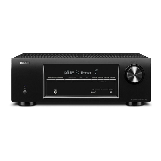
AVR-1513
• For purposes of improvement, specifications and design are subject to change without notice.
• Please use this service manual with referring to the operating instructions without fail.
• Some illustrations using in this service manual are slightly different from the actual set.
S0422-0V01DM/DG1202
SERVICE MANUAL
MODEL
AV SURROUND RECEIVER
Copyright 2012 D&M Holdings Inc. All rights reserved.
WARNING: Violators will be prosecuted to the maximum extent possible.
JP
E3
E2
P P
e
D&M Holdings Inc.
Ver. 1
EK
EA
E1C E1K
P
CI
Advertisement
Table of Contents

Related Manuals for Denon AVR-1513


Summary of Contents for Denon AVR-1513
-
Page 1: Service Manual
Ver. 1 SERVICE MANUAL MODEL E1C E1K AVR-1513 AV SURROUND RECEIVER • For purposes of improvement, specifications and design are subject to change without notice. • Please use this service manual with referring to the operating instructions without fail. • Some illustrations using in this service manual are slightly different from the actual set. -
Page 2: Table Of Contents
SCHEMATIC DIAGRAMS ............76 CONTENTS FRONT PART ................76 POWER PART ................77 ABOUT THIS MANUAL .............3 MAIN PART ................78 What you can do with this manual ..........3 INPUT & VOLUME PART ............79 Using Adobe Reader (Windows version) ........4 VIDEO PART (PRE OUT-SUBWOOFER) .......80 SAFETY PRECAUTIONS ............6 DSP PART ................81 NOTE FOR SCHEMATIC DIAGRAM .........7... -
Page 3: About This Manual
ABOUT THIS MANUAL Read the following information before using the service manual. What you can do with this manual Search for a Ref. No. (phrase) Jump to the target of a schematic diagram (Ctrl+Shift+F) connector You can use the search function in Acrobat Reader to Click the Ref. -
Page 4: Using Adobe Reader (Windows Version)
Using Adobe Reader (Windows version) Add notes to this data (Sign) Magnify schematic / printed wiring board diagrams - 1 The Sign function lets you add notes to the data in this manual. (Ctrl+Space, mouse operation) Save the file once you have finished adding notes. Press Ctrl+Space on the keyboard and drag the mouse to select the area you want to view. - Page 5 Magnify schematic / printed wiring board Magnify schematic / printed wiring board diagrams - 2 diagrams - 3 (Pan & Zoom function) (Loupe Tool function) The Pan & Zoom function lets you see which part of a The Loupe Tool function lets you magnify a specific magnified diagram is being shown in a separate window.
-
Page 6: Safety Precautions
SAFETY PRECAUTIONS The following items should be checked for continued protection of the customer and the service technician. LEAKAGE CURRENT CHECK Before returning the set to the customer, be sure to carry out either (1) a leakage current check or (2) a line to chassis resistance check. -
Page 7: Note For Schematic Diagram
NOTE FOR SCHEMATIC DIAGRAM WARNING: Parts indicated by the z mark have critical characteristics. Use ONLY replacement parts recommended by the manufacturer. CAUTION: Before returning the set to the customer, be sure to carry out either (1) a leakage current check or (2) a line to chassis resistance check. If the leakage current exceeds 0.5 milliamps, or if the resistance from chassis to either side of the power cord is less than 460 kohms, the set is defective. -
Page 8: Technical Specifications
TECHNICAL SPECIFICATIONS n Audio Section n Tuner section • Power amplifier [FM](Note: μV at 75 Ω, 0 dBf = 1 x 10 –15 Rated output : Receiving Range (for E3) : Front : [FM] 87.5 MHz – 107.9 MHz [AM]520 kHz – 1710 kHz 75 W + 75 W (8 Ω, 20 Hz –... -
Page 9: Caution In Servicing
SOURCE SELECT 1 Service Jig When you update the firmware, you can use the following JIG (RS232C to internal connector conversion adapter). Please order it from Denon Official Service Distributor in your region if necessary. 8U-210100S WRITING KIT 1 Set 606050028012P : 7P FFC(1.0) L-240... -
Page 10: Disassembly
DISASSEMBLY • Disassemble in order of the arrow in the following figure. • In the case of the re-assembling, assemble it in order of the reverse of the following flow. • In the case of the reassembling, observe "Caution concerning disassembly and assembly!". •... - Page 11 About the photos used for "descriptions of the DISASSEMBLY" section • The shooting direction of each photograph used herein is indicated on the left side of the respective photograph as "Shooting direction: ***". (*** : A,B,C,D) • Refer to the diagram below about the shooting direction of each photograph. •...
-
Page 12: Front Panel Assy
1. FRONT PANEL ASSY Proceeding : FRONT PANEL ASSY CABINET TOP → (1) Remove the screws. View from the bottom (2) Remove the screws and disconnect the FFC. FRONT PANEL ASSY (3) Disconnect the connector wires. CN102 CN104 Please refer to "EXPLODED VIEW" for the disassembly method of each PCB included in FRONT PANEL ASSY. -
Page 13: Digital Pcb Assy
2. DIGITAL PCB ASSY Proceeding : CABINET TOP DIGITAL PCB ASSY → (1) Remove the screws. Shooting direction: A (2) Remove the screws. Disconnect the connector wires and FFC then disconnect the TUNER PCB. CN90 CN205 CN95 TUNER PCB CN202 DIGITAL PCB... -
Page 14: Radiator Assy
3. RADIATOR ASSY Proceeding : CABINET TOP DIGITAL PCB ASSY RADIATOR ASSY → → (1) Remove the screws. Shooting direction: A (2) Remove the screws then disconnect the connector wire. Remove the RADIATOR ASSY from the CHASSIS BOTTOM. MAIN PCB CN503... -
Page 15: Power Pcb
4. POWER PCB Proceeding : CABINET TOP POWER PCB → Please refer to "EXPLODED VIEW" for the disassembly method of POWER PCB. 5. REGULATOR PCB Proceeding : CABINET TOP REGULATOR PCB → Please refer to "EXPLODED VIEW" for the disassembly method of REGULATOR PCB. 6. -
Page 16: Special Mode
SPECIAL MODE Special mode setting button b Press the X button to turn on the power while pressing both the button A and the button B at the same time. Mode Button A Button B Contents Firmware versions such as Main, DSP or OSD are displayed µcom/DSP/OSD Version display STATUS DIMMER... -
Page 17: Μcom/Dsp/Osd Version Display Mode
Model destination information → w Main-µcom version → e DSP version → r OSD version Display State q Model destination information AVR-1513 E3 model A V R 1 5 1 3 AVR-1513 E2 model A V R 1 5 1 3... -
Page 18: When The Microprocessor Is Replaced With A New One
WHEN THE MICROPROCESSOR IS REPLACED WITH A NEW ONE When the U-PRO (Microprocessor) or the Flash ROM is replaced, confirm the following. After PWB Name Ref. No. Description Remark replaced DIGITAL IC91 STM32F101ZE SOFTWARE: Main DIGITAL IC82 MX25L8006EM2I-12G SOFTWARE: DSP ROM DIGITAL IC14 MX25L8006EM2I-12G... - Page 19 1.3. INSTALL UPDATE TOOL (1) Click the "ST_Flash_Loder" folder. (2) Run the "Flash_Loader_Demonstrator_v2.4.0_Setup.exe" on program file. The following screen will be displayed. The Setup Status bar appears.
- Page 20 (3) Click the "Next" button. (4) Click the "Yes" button.
- Page 21 (5) Click the "Next" button after inputting "User Name" and "Company Name". (6) Click the "Next" button. The following screen will be displayed. The Setup Status bar appears.
- Page 22 (7) Click the "Finish" button.
-
Page 23: Update Firmware
2. UPDATE FIRMWARE (1) Connect the update terminal of AV receiver with the "WRITING KIT". (2) Set the switch of "WRITING KIT". (Refer to the table below.) DSPBOOT CNVSS (3) Press the X button to turn the power on of AV receiver. (4) Set the switch of "WRITING KIT". - Page 24 Click the “Next” button for 2nd time. Click the “Next” button for 3rd time.
- Page 25 (8) Choose Flash File(DSP1). Click the following button. From the file browser windows select file of "AVR1513_SF_DSP1(x.x.x).bin". Click the "Open" button.
- Page 26 Click the “Next” button. The following screen will be displayed. The Setup Status bar appears.
- Page 27 The following screen will be displayed and click the "Close" button.
- Page 28 (9) Set the switch of "WRITING KIT". (Refer to the table below.) DSPBOOT CNVSS (10) Press the "RESET" switch of "WRITING KIT". Wait for about 130 seconds until "Write Complete." is displayed on VFD. (11) Set the switch of "WRITING KIT". (Refer to the table below.) DSPBOOT CNVSS (12) Press the "RESET"...
- Page 29 Click the “Next” button for 2nd time. Click the “Next” button for 3rd time.
- Page 30 (15) Choose Flash File(DSP2). Click the following button. From the file browser windows select file of "AVR1513_SF_DSP2(x.x.x).bin". Click the "Open" button.
- Page 31 Click the “Next” button. The following screen will be displayed. The Setup Status bar appears.
- Page 32 The following screen will be displayed and click the "Close" button.
- Page 33 (16) Set the switch of "WRITING KIT". (Refer to the table below.) DSPBOOT CNVSS (17) Press the "RESET" switch of "WRITING KIT". Wait for about 100 seconds until "Write Complete." is displayed on VFD. (18) Set the switch of "WRITING KIT" (Refer to the table below). DSPBOOT CNVSS (19) Press the "RESET"...
- Page 34 Click the “Next” button for 2nd time. Click the “Next” at 3rd time.
- Page 35 (22) Choose Flash File(OSD). Click the following button. From the file browser windows select file of "AVR1513_SF_OSD(vxx.x.x).bin". Click the "Open" button.
- Page 36 Click the “Next” button. The following screen will be displayed. The Setup Status bar appears.
- Page 37 The following screen will be displayed and click the "Close" button.
- Page 38 (23) Set the switch of "WRITING KIT". (Refer to the table below.) DSPBOOT CNVSS (24) Press the "RESET" switch of "WRITING KIT". Wait for about 30 seconds until "Write Complete." is displayed on VFD. (25) Set the switch of "WRITING KIT". (Refer to the table below.) DSPBOOT CNVSS (26) Press the "RESET"...
- Page 39 Click the “Next” button for 2nd time. Click the “Next” button for 3rd time.
- Page 40 (29) Choose Flash File(MAIN). Click the following button. From the file browser windows select file of "AVR1513_MCU(vxx.x.x).bin". Click the "Open" button.
- Page 41 Click the “Next” button. The following screen will be displayed. The Setup Status bar appears.
-
Page 42: Notice
The following screen will be displayed and click the "Close" button. (30) Set the switch of “Writing Kit". (Refer to the table below.) DSPBOOT CNVSS (31) Press the "RESET" switch of “Writing Kit". (32) Initializing. 1. Turn off the power using X button. 2. -
Page 43: Adjustment
ADJUSTMENT Audio Section Adjusting Idling Current Required measurement equipment: DC Voltmeter 1. Preparation (1) Avoid direct blow from an air conditioner or an electric fan and humidity should be moderate, and place the set at normal usage environment. Temperature should be at 15 °C ~ 30 °C (59 °F ~ 86 °F). (2) Presetting •... -
Page 44: Surround Modes And Parameters
SURROUND MODES AND PARAMETERS... -
Page 47: Trouble Shooting
TROUBLE SHOOTING 1. POWER 1.1. Power not turn on Power not turn on. Are there any incomplete Is the ON/STANDBY connections in the Is there a short circuit Correct the short connectors connecting between the speaker circuit between the indicator on the front panel flashing red? between the various circuit terminals and the ground? -
Page 48: Analog Video
2. Analog video MONITOR OUT(CVBS) Output NG Check ±5VV The power supply circuitry is +5VV : C755 defective. -5VV : C754 Check input Check pattern from JK71 to IC71 and Check output (When the SAT/CBL function) check cable between AMP and player or Output V : IC71-1pin Vin3 : IC71-7pin... -
Page 49: Hdmi/Dvi
(6) Is the BD/DVD player's HDMI output setting correct? the BD/DVD player's operating instructions. (7) When you use a DENON BD/DVD player's, is the fluorescent display tube's "HDMI" indicator lit? If you use a non-DENON BD/ DVD player's, proceed to "YES". - Page 50 BD/DVD player is connected. (JK11/JK12/JK13/JK51) display's "HDMI" indicator lit? Is communication waveform confirmed in Test to the IC11,IC51 are If using a non-DENON BD/ point (DDC_CLK/DDC_DATA)? defective. DVD player, proceed to "NO". Is terminate the TMDS signal is 3.3V confirmed of Replace the IC11,IC51.
- Page 51 (19) Check power supply. The power supply circuitry is defective. Are 1.8V or 3.3V supplied to IC11 (each power supply pin)? The X101 or IC11 is defective. (20) Check xtal oscillator. Replace the new parts. Is there 28.6363MHz oscillation of X101? (21) Check RESET.
- Page 52 3.2. HDMI test point and waveforms MONITOR SAT/CBL SAT/CBL COAX IN DVD IN GAME MONITOR SAT/CBL OPT IN R146 R145 R106 R171 R111 R172 D142 D141 D101 D102 D111 D112 C931 C932 R659 R183 CN91 R173 D122 R116 D906 D121 R191 JK81 R768...
- Page 53 DDC_CLK/DDC_DATA/TMDS : Check items (16),(18) 0.9V DDC_CLK 2.48V TMDS SIGNAL DDC_DATA DVDD/XTAL/RESET/SCL : Check items (19),(20),(21) P-ON HDMI_SDA/SCL(I2C) : Check item (22) HDMI_SDA HDMI_SCL...
-
Page 54: Audio
4. AUDIO 4.1. AUDIO CHECK AUDIO OUTPUT : NG INPUT SURROND MODE SOURCE CHECK1 Check ANALOG AUDIO BLOCK. ANALOG 2CH DIRECT ANALOG INPUT SURROND MODE SOURCE CHECK2 Check Digital AUDIO BLOCK. COAX or OPT Legacy(PCM or DolbyDigital or dts…) INPUT SURROND MODE SOURCE CHECK3 Check via AD. - Page 55 4.2. Power AMP (MAIN UNIT) No sound is output. The protector operates. Is the power transistor open or short- circuited? Replace the power transistor. 2SB1560/2SD2390 Is the emitter resistance of the power transistor open? Replace the emitter resistance. 0.47Ω Is the base resistance of the power transistor open? Replace the base resistance.
- Page 56 Personal notes:...
-
Page 57: Clock Flow & Wave Form In Digital Block
CLOCK FLOW & WAVE FORM IN DIGITAL BLOCK IC11 Wave form ADV7623BSTZ CH1: RXP2 IC84 CS42528 (DIR+CODEC) RMCK(55) Coaxial1 (47)RXP2/GPO2 (49)RXP0 Optical1 (32)DAI2_LRCK SAI_SCLK(61) IC81 SAI_LRCK(60) (33)DAI2_SCLK CS497024CVZ (34)DAI2_DATA,DSD5 (AUDIO DSP) SAI_SDOUT(54) CH1: SDOUT CH2: LRCLK2 CH3: SCLK2 Test point Detail A MONITOR SAT/CBL... -
Page 58: Analog Audio/Video Block Diagram
ANALOG AUDIO/VIDEO BLOCK DIAGRAM H/P OUT H/P L H/P R MAIN AMP 2SD2390/2SB1560 SPK OUT ANA_FL DA_FL ANA_FR DA_FR MAIN DA_CEN AUDIO IN SAT/CBL DA_SW PORTABLE(FRONT) DA_SL DA_SR TUNER DA_SBL FM/AM DA_SBR VOL IC NJU72340A AD_FL PRE OUT AD_FR MUTE TO DIGITAL AUDIO BLOCK DA01... -
Page 59: Digital Audio/Hdmi Block Diagram
DIGITAL AUDIO/HDMI BLOCK DIAGRAM DA_FL DIR/CODEC CS42528 DA_FR LRCK DA_CEN SCLK DA_SW CODEC VOLUME DIGITAL DIGTAL IN SERIAL CONTROL FILTER ANALOG DA_SL PORT FILTER OPTICAL IN1 DA_SR COAXIAL IN1 GAIN DIGITAL & FILTER CLIP SERIAL GAIN DATA DIGITAL SERIAL & FILTER CLIP AUDIO I/F... -
Page 60: Power Block Diagram
POWER BLOCK DIAGRAM MAIN+B POWER RELAY 47.1mA S1(AMP+B,-B) GBJ806 VOLUME IC(NJU72340A) MAIN-B 25mA MTZ7.5B OPAMP x 1 Portable IN 7.5mA OPAMP x 3 D/A OUT 21mA RELAY*4 145.1mA NJM7812 VOLUME(NJU72340A) S2(+12V,-12V) MTZ7.5B NJM2595 KIA7905PI S2 TOTAL : 370.2mA OPAMP NJM7912 OPEN TUNER 50mA... -
Page 61: Level Diagram
LEVEL DIAGRAM FRONT ch A/D IN A/D IN D/A OUT ELECTRIC PRE AMP1 POWER AMP REV AMP REV AMP VOLUME AUDIO IN SPK OUT FRONT NJU72340AFH3 DIGITAL H/P OUT CS42528 FRONT 40dB 40dB 30dB 30dB CS42528 SPK OUT DIFF. INPUT CS42528 FRONT 0dBFS=5.6Vpp... - Page 62 CENTER ch D/A OUT ELECTRIC PRE AMP1 POWER AMP VOLUME SPK OUT DSP OUT CENTER NJU72340AFH3 CENTER 40dB 40dB 30dB 30dB SPK OUT CS42528 FRONT DIFF. OUT 4.47Vrms/8ohm 0dBFS=5Vpp FULL SCALE LEVEL=2Vrms 20dB =1.77Vrms 20dB DOLBY LIMIT LEVEL (ALL ch-3dBFS) 0dBFS +29dB 10dB...
- Page 63 SURROUND ch D/A OUT ELECTRIC PRE AMP1 POWER AMP VOLUME SPK OUT DSP OUT SURROUND NJU72340AFH3 SURROUND 40dB 40dB 30dB 30dB SPK OUT CS42528 FRONT DIFF. OUT 4.47Vrms/8ohm 0dBFS=5Vpp FULL SCALE LEVEL=2Vrms 20dB =1.77Vrms 20dB DOLBY LIMIT LEVEL (ALL ch-3dBFS) 0dBFS +29dB 10dB...
- Page 64 SUBWOOFER ch D/A OUT SW SUM ELECTRIC REV AMP PRE AMP1 REV AMP VOLUME DSP OUT SW WOOFER PREOUT NJU72340AFH3 MUTE SUBWOOFER 40dB 40dB 30dB 30dB CS42528 DIFF. OUT 0dBFS=5Vpp FULL SCALE LEVEL=2Vrms 20dB =1.77Vrms 20dB DOLBY LIMIT LEVEL (ALL ch-3dBFS) 0dBFS PREOUT 10dB...
-
Page 65: Wiring Diagram
WIRING DIAGRAM AC CORD DIGITAL PCB POWER<-AC IN BN99 CN9B BN94 CN204 POWER<-DIGITAL CN97 CN90 CN95 TUNER CN203 REGUL.<- DIGITAL REGULATOR PCB POWER PCB CN503 BN501 BN502 MAIN PCB BN505 TRANS POWER->MAIN CN102 TRANS CN101 POWER FRONT PCB CN103 BN13A BN11A TRANS POWER ->... -
Page 66: Printed Wiring Boards
PRINTED WIRING BOARDS MAIN (COMPONENT SIDE) J5601 D5704 C5708 D5703 BK501 C5706 R5714 BN5703_2 J5628 JK504 JK503 J5656 J5677 J5655 C5717 J5629 BN5705_2 J5630 C5711 C5713 J5657 R5706 R5708 J5658 R5715 J5631 BN5707_2 R5718 J5632 C5609 C5612 C5610 C5613 R5725 C5614 C5611 R5716... - Page 67 MAIN (FOIL SIDE) C5617 C5616 C5620 C5619 Q5706 Q5703 Q5707 Q5704 Q5708 Q5705 Q5701 Q5601 Q5603 Q5604 Q5602 BN501 BN502 Q5508 Q5507 Q5408 Q5407 Q5308 Q5307 Q5208 Q5207 Q5108 Q5107 R5526 R5426 R5326 R5226 R5126 鉛フリー半田 半田付けには、鉛フリー半田 (Sn-Ag-Cu) を使用してください。 Lead-free Solder When soldering, use the Lead-free Solder (Sn-Ag-Cu).
-
Page 68: Tuner
TUNER TUNER PORTABLE PORTABLE (COMPONENT SIDE) (FOIL SIDE) (COMPONENT SIDE) (FOIL SIDE) C1060 BN11B JK102 CUP12425Z_2 NO PARTS *TUNER MODULE OPTION. *TUNER MODULE OPTION. BN508 BN508 AVR1513 E3 R5601 AVR1513 E3 R5601 AVR1513 E2 R5602 AVR1513 E2 R5602 AVR1513 E1C R5603 AVR1513 E1C R5603... -
Page 69: Front
FRONT (COMPONENT SIDE) F1001 NO PARTS NO PARTS T 100mA L 250V LUG11 1513 = 23P R1066 NO PARTS CN101 FL101 Q1005 C1007 NO PARTS 1613/1713 = 25P C1075 J1052 J1042 D1007 C1008 J1019 NO PARTS J1043 J1044 J1050 J1020 C1006 CN102 J1021... -
Page 70: Digital
DIGITAL (COMPONENT SIDE) MONITOR SAT/CBL SAT/CBL COAX IN DVD IN MONITOR GAME SAT/CBL OPT IN R146 R145 R106 R171 R111 R172 D142 D141 D101 D102 D111 D112 C931 C932 R659 R183 CN91 R173 D122 R116 D906 D121 R191 JK81 R768 JK15 R179 JK11... - Page 71 DIGITAL (FOIL SIDE) 1.CH_GND 2.CH_GND R205 R216 R203 R767 D915 D912 R212 R218 R220 C635 R214 R222 R632 C306 R631 R759 D919 C166 R643 3.CH_GND L115 R642 4.INT C134 R227 R228 C130 L101 C163 5./RST R748 R225 R226 C647 R223 R224 6./CE 7.SDIO...
-
Page 72: F-Hdmi
F-HDMI POWER (COMPONENT SIDE) (COMPONENT SIDE) D155 C533 C529 C530 CN205 R502 ADJ-1 ADJ-2 C500 L500 R513 R512 R520 R519 R524 CN204 IC51 J9008 C519 BK11 C525 C531 Q2001 Q2003 C521 C511 C532 C534 CUP12426Z-2 F-HDMI TEST J9007 CN203 F2001 ET201 C2039 NEUTRAL... - Page 73 POWER (FOIL SIDE) NEUTRAL LIVE Q2002 C2031 C2033 DIPPING DIPPING IN 鉛フリー半田 半田付けには、鉛フリー半田 (Sn-Ag-Cu) を使用してください。 Lead-free Solder When soldering, use the Lead-free Solder (Sn-Ag-Cu).
-
Page 74: Regulator
REGULATOR (COMPONENT SIDE) POWER PCB BK203 LUG21 REGULATOR PART CUP12424Z_A C2002 C2008 CN202 J2004 C2007 C2001 C2006 CN201 C2014 R2005 1.S2_AC 2.S2_GND R2006 3.S2_AC 4.N.C R2004 D2008 5.S3_AC C2009 6.DGND R2003 D2006 7.S3_AC C2021 C2017 D2005 J2018 C2004 J2013 J2021 C2013 R2001 C2003... - Page 75 REGULATOR (FOIL SIDE) -12V C2015 C2012 C2010 C2016 +12V 鉛フリー半田 半田付けには、鉛フリー半田 (Sn-Ag-Cu) を使用してください。 Lead-free Solder When soldering, use the Lead-free Solder (Sn-Ag-Cu).
-
Page 76: Schematic Diagrams
TO CN97 DIGITAL PART AVR1513 5.PORTABLE_L 25p -AVR1613/AVR1713 AVR1613/1713 : 5.MIC_SIGNAL 1.25mm 25PIN FFC AVR1513/AVR1613/1713/1723 FRONT PART AVR1513/AVR1613/1713/1723 FRONT PART FROM DIGITAL B'D 23p -AVR1513 1.25mm 23PIN FFC CN101 CN101 FROM DIGITAL B'D CJP25GB286ZN CFL18BT021GINK FL101 LUG11 RC101 1613/1713 ONLY D1001 R1066 F1001... -
Page 77: Power Part
REGULATOR R2001 0.47 R2002 0.47 CN201 R2003 7. S3_AC CN202 0.47 CN202 6. DGND R2038 R2004 VGND 5. S3_AC OPEN 0.47 +5VH 4. N.C R2005 D2001 +5VH 3. S2_AC 0.22 CVD1N4007ST DGND 2. S2_GND R2006 D2002 DGND 1.. S2_AC 0.22 CVD1N4007ST +5VD +5VD... -
Page 78: Main Part
AVR1513/AVR1613/1713 MAIN PART PTC Thermistors D5101 R5115 R5116 R5126 OPEN R5103 R5108 470K 5.6K(1W) 5.6K(1W) B59641A0095A062 C5103 C5106 33P R5117 C5109 LEFT FRONT-CH 4R7(1W) 0.1uF Q5107 Q5105 BC3-12H MMBT5401 2SD2390 R5123 RY560 C5101 R5102 Q5101 R5109 33K FL_IN Q5104 D5102 +12V KSA992FTA KTC3114A... -
Page 79: Input & Volume Part
INPUT & VOLUME PART AGND MINI_L MINI_R MCUGND DAC_MUTE MAIN_VOL_CLK MAIN_VOL_DATA R637 TUNER_INT R651 TUNER_RST R653 TUNER_CE R656 TUNER_SDIO R657 TUNER_SCLK +12V CN96 CN96 -12V CH_GND IC70 OPEN CH_GND R957 CH_GND OPEN BD61 CLZ9R005Z R639 AGND /RST -12V R640 MUTE_+B SDIO SCLK +5VV... -
Page 80: Video Part (Pre Out-Subwoofer)
VIDEO PART ( PRE OUT-SUBWOOFER ) TO K FROM DSP PART NLM2595 S/W TABLE(SW2,5 CONTROL) FUNC.IN (14) (10) MUTE X (L) SAT/CBL R760 JK71 1.8K R766 MONITOR OUT 82(1%) DVD IN 10/50V C764 SAT/CBL IN CJJ4P076Z 10/50V C763 R768 CVBS_SW2 CVBS_SW5 SUB_MUTE MCUGND... -
Page 81: Dsp Part
TO E CODEC_MUTE DSP_MODE_SEL TO F TO INPUT PART DIR_CE DIR_RST DIR_MOSI TO VIDEO PART DIR_CLK DIR_MISO HDMI_SW DSP_CS DSP_SPC1_IRQ DSP_PCP_BSY DSP_RST DSP_MOSI DSP_MISO DSP_CLK +3V3D SD[0:7] C972 OPEN OPEN +3V3D DSP PART C973 AD[0:19] OPEN DSP_AUDIO C937 OPEN C938 +3V3D D+1.8V +3V3D... -
Page 82: Mcu Part
TO CN101 FOR UPDATE TO FRONT B'D MCU PART CN97 CN97 CN91 CJP23GA115ZY CJP07GB113ZY 0ohm start EMC test Q914 AGND C940 C941 OPEN OPEN 0.1uF MINI_L MINI_R MCUGND Q915 OPEN Q917 DAC_MUTE OPEN DAC_MUTE MAIN_VOL_CLK MAIN_VOL_CLK MAIN_VOL_DATA MAIN_VOL_DATA TUNER_INT Q916 TUNER_INT OPEN TUNER_RST... -
Page 83: Hdmi Part
0.01uF OPEN(ADI RECOMMENDATION) HDMI PART TXEN HDMI_MCLK CVDD DVDD DVDDIO PVDD TVDD TXPLVDD TXAVDD TXPVDD HDMI_SCLK HDMI_LRCLK HDMI_TXEN HDMI_MCLK HDMI_SDATA3 HDMI_SCLK HDMI_SDATA2 HDMI_LRCLK HDMI_SDATA3 HDMI_SDATA1 HDMI_SDATA2 HDMI_SDATA0 HDMI_SDATA1 HDMI_SDATA0 R167 OPEN CEC_COM +5VH CEC_5V +5VH CN9B +3V3H CN9B DGND CJP23GA193ZY HDMI_RST 10022H-23C +3V3H... -
Page 84: Front-Hdmi In Part
OPEN R507 OPEN IC52 OPEN VCCA VCCB FRONT-HDMI IN PART SCLA SCLB SDAA SDAB PCA9507DP R523 Q500 Q501 RT1P141C R501 RT1N241C R521 R525 R526 C500 19.HP DET JK51 OPEN R502 18.+5V 17.GND 16.DDC DATA D154 OPEN 15.DDC CLK CEC5V 14.NC L500 13.CEC 12.CK-... -
Page 85: Exploded View
EXPLODED VIEW C4-1 C3-1 C4-2 C2-5 C1-1 C2-2 C2-3 C2-4 C2-1 C1-6 C1-2 C1-3 C1-5 C1-4 C3-2 WARNING: Parts marked with this symbol have critical characteristics. Use ONLY replacement parts recommended by the manufacturer. 印の部分は安全を維持するために重要 な部品です。従って交換時は必ず指定の 部品を使用してください。... - Page 86 Personal notes: Personal notes:...
-
Page 87: Parts List Of Exploded View
PARTS LIST OF EXPLODED VIEW z Parts indicated by "nsp" on this table cannot be supplied. z P.W.B. ASS'Y indicated by "nsp" on this table cannot be supplied. When repairing the P.W.B. ASS'Y, check the board parts list and order replacement parts. z Parts indicated by the "... - Page 88 Ref. No. Part No. Part Name Remarks Q'ty New 943412100720D KNOB,VOLUME CBN1A263C73 943446100590D PLATE,VOLUMEKNOB CGX1A469 42151002100AD DENON BADGE CGB1A247H67 42151002101AD DENON BADGE 943402102050D PANEL,FRONT CGW1A519RHZB63 943402102060D PANEL,FRONT CGW1A519RHYB63 943402102070D PANEL,FRONT BKE1C CGW1A519RHXB63 943402102080D PANEL,FRONT SPE1C CGW1A519RGZG45 943423100310D INDICATOR,POWER CGL1A299 943411101750D...
- Page 89 Ref. No. Part No. Part Name Remarks Q'ty New SCREW CTW3+8JR SCREW CTW3+12JR SCREW,TRANS CHDR1A023R SCREW CTBD3+8JFZR SCREW CTBD3+8JFN SCREW CTB3+8JFZR SCREW CTB3+8JFN SCREW CTB3+6FR SCREW CTW3+6JR SCREW,SPECIAL CHD4A012R WIRES ★ H1 943606501530S CARD,CABLE 23P, L=180mm CWC5C4A23B180B10 ★ H2 943606501540S CARD,CABLE 23P, L=330mm CWC5F4A23A330B08...
-
Page 90: Packing View
PACKING VIEW 5-10 5-11 PARTS LIST OF PACKING & ACCESSORIES z Parts indicated by "nsp" on this table cannot be supplied. z Parts indicated by the " ★ " mark are not illustrated in the exploded view. z The parts listed below are only for maintenance. Therefore they might differ from the parts used in the unit in appearances or dimensions. Note: The symbols in the column "Remarks"... - Page 91 Ref. No. Part No. Part Name Remarks Q'ty New 943533101130D PAD,SNOW(R) CPS1A917 INSTRUCTIONMANUALASS'Y BATTERY,AAA2PCSINPACK CABR03PPB 35201007100AD CDMANUALASS'Y CFT1A049ZA 35201007200AD CDMANUALASS'Y CFT1A050ZA 35201007300AD CDMANUALASS'Y CFT1A051ZA BAG,POLY(MANUAL) CPB1A197Z LABEL,BARCODE(MANUAL) CQB1A971 LIST,S.S CQE1A226P CARD,WARRANTY CQE1A224Q CARDFORCHINAINDENTIFICATION CQE1A450Z 54111092800AD SAFETY INSTRUCTIONS (E3) CQE1A547Z 54111093000AD SAFETY INSTRUCTIONS (E2) CQE1A549Z 54111093100AD...
-
Page 92: Semiconductors
SEMICONDUCTORS Only major semiconductors are shown. General semiconductors etc. are omitted from list. The semiconductors which have a detailed drawing in a schematic diagram are omitted from list. 1. IC's NJU72340A (DIGITAL :IC61) NJU72340A Terminal Functions... -
Page 93: Pin Assignment
G Package Outline DIP16,DMP16 I PIN CONFIGURATION and BLOCK DIAGRAM NJM2595M (DIGITAL : IC71) Vin1 Vin2 75Ω Vout1 Driver Vin3 75Ω Vout2 Vin4 Driver Vin5 75Ω Vout3 Driver TC74VHC157F/FN/FT/FK Pin Assignment IEC Logic Symbol TC74VHC157FT (DIGITAL : IC85) - 1 - (15) SELECT SELECT... - Page 94 CS42528 (DIGITAL : IC84) CS42528 Block diagram...
- Page 95 CS42528 Terminal Functions...
- Page 96 CS497024CVZ (DIGITAL : IC81)
- Page 97 CS497024CVZ Block diagram M12L16161A5TG (DIGITAL : IC83) M12L16161A5TG Terminal Functions Name Input Function System Clock Active on the positive going edge to sample all inputs. Disables or enables device operation by masking or enabling all inputs except CLK, CKE Chip Select and L(U)DQM.
- Page 98 STM32F101xC, STM32F101xD, STM32F101xE Pinouts and pin descriptions Pinouts and pin descriptions STM32F101ZE (DIGITAL : IC91) Figure 3. STM32F101xC, STM32F101xD and STM32F101xE access line LQFP144 pinout DD_2 SS_2 PA13 PA12 VBAT PA11 PC13-TAMPER-RTC PA10 PC14-OSC32_IN PC15-OSC32_OUT DD_9 SS_9 SS_5 LQFP144 DD_5 PF10 OSC_IN PD15...
- Page 99 Pin Name Symbol Pullup STBY stop Function 36 PA2 O(L) 37 PA3 O(L) 38 VSS_4 39 VDD_4 3.3V 40 PA4 DSP_CS O/L DSP Chip Select 41 PA5 DSP_CLK D3VPu O/L DSP_CLK 42 PA6 DSP_MISO D3VPu O/L DSP MISO 43 PA7 DSP_MOSI O/L DSP MOSI 44 PC4...
- Page 100 Pin Name Symbol Pullup STBY stop Function 102 PA10 UPDATE_RX O/L UPDATE RX 103 PA11 RESERVED O(L) RESERVED 104 PA12 RESERVED O(L) RESERVED 105 PA13 DEBUG JTMS / SWDIO 106 PCAP_2 Not Connected 107 VSS_2 108 VDD_2 3.3V 109 PA14 DEBUG JTCK / SWCLK 110 PA15...
-
Page 101: Pin Description
Pin Description ADV7623 (DIGITAL : IC11) DDCC_SCL 108 DDCA_SDA CVDD 107 RTERM CGND 106 5V_DETA RXC_C- 105 HP_CTRLA RXC_C+ 104 PGND TVDD 103 PVDD RXC_0- 102 XTAL1 RXC_0+ 101 XTAL CGND 100 PVDD RXC_1- 10 99 PGND RXC_1+ 11 98 PWRDNB TVDD 12 97 RESETB RXC_2- 13... - Page 102 ADV7623 Hardware Manual ADV7623 Terminal Functions Table 6. Function Descriptions Location Mnemonic Type Description DDCC_SCL Digital Input HDCP slave serial clock port C. DDCC_SCL is a 3.3 V input that is 5 V tolerant. CVDD Power Receiver comparator supply voltage (1.8V) CGND Ground TVDD and CVDD Ground...
- Page 103 ADV7623 Hardware Manual Location Mnemonic Type Description D in the HDMI interface. RXD_0+ HDMI Input Digital input channel 0 True of port D in the HDMI interface. CGND Ground TVDD and CVDD Ground RXD_1- HDMI Input Digital input channel 1 complement of port D in the HDMI interface.
- Page 104 ADV7623 Hardware Manual Location Mnemonic Type Description TXGND Ground TXAVDD Ground TX0- HDMI Output Differential Output Channel 0 Complement. Differential output of the red data at 10× the pixel clock rate; supports TMDS logic level. TX0+ HDMI Output Differential Output Channel 0 True. Differential output of the red data at 10×...
- Page 105 ADV7623 Hardware Manual Location Mnemonic Type Description MCLK_IN Digital Input Audio Reference Clock. 128 × N × fs with N = 1, 2, 3, or 4. Set to 128 × sampling frequency (fs), 256 × fs, 384 × fs, or 512 × fs.
- Page 106 ADV7623 Hardware Manual Location Mnemonic Type Description AP0_OUT Digital Output Audio output port 0. AP1_OUT Digital Output Audio output port 1. AP2_OUT Digital Output Audio output port 2. AP3_OUT Digital Output Audio output port 3. AP4_OUT Digital Output Audio output port 4. DGND Ground Ground for DVDD...
- Page 107 ADV7623 Hardware Manual Location Mnemonic Type Description CGND Ground TVDD and CVDD Ground RXA_C- HDMI Input Digital input clock Complement of port A in the HDMI interface. RXA_C+ HDMI Input Digital input clock True of port A in the HDMI interface. TVDD Power Receiver terminator supply voltage (3.3 V)
- Page 108 ADV7623 Hardware Manual Location Mnemonic Type Description B in the HDMI interface. RXB_1+ HDMI Input Digital input channel 1 true of port B in the HDMI interface. TVDD Power Receiver terminator supply voltage (3.3 V) RXB_2- HDMI Input Digital input channel 2 complement of port B in the HDMI interface.
- Page 109 AD8195 (F-HDMI : IC51) 30 AVCC PIN 1 29 PE_EN INDICATOR 28 TX_EN 27 AVEE 30 AVCC PIN 1 VTTI 26 AVCC AD8195 29 PE_EN INDICATOR 28 TX_EN 25 AVCC TOP VIEW (Not to Scale) 27 AVEE 24 AVEE VTTI 26 AVCC AD8195 23 AVCC...
- Page 110 Temp Rating EX3AV Part Number (° C) Package EX3AV -40 to +85 38-pin QFN T&R EX3AV (DIGITAL : IC16) T&R Figure 3: Pinout Diagram (Top View) NOTE: All perimeter pins must be soldered to PCB. Figure 3: Pinout Diagram (Top View) EX3AV Terminal Functions NOTE: All perimeter pins must be soldered to PCB.
-
Page 111: Fl Display
2. FL DISPLAY FLD (018BT021GINK) (FRONT : FL101) PIN CONNECTION GRID ASSIGNMENT... - Page 112 ANODE CONNECTION...
-
Page 113: Parts List Of P.c.b. Unit
PARTS LIST OF P.C.B. UNIT z Parts indicated by "nsp" on this table cannot be supplied. z The parts listed below are only for maintenance. Therefore they might differ from the parts used in the unit in appearances or dimensions. Note: The symbols in the column "Remarks"... - Page 114 Ref. No. Part No. Part Name Remarks Q'ty CAPACITORS GROUP C1002 CAP,MYLAR(100V/0.1uF/J) HCQI1H104JZT C1003 CAP,ELECT(50V/10uF)-S CCEA1HKS100T C1004 943134010530S CAP,ELECT(50V/1uF) CCEA1HH1R0T C1005 00MOA22706320 CAP,ELECT(63V/220uF) CCEA1JH221E C1006 943134010530S CAP,ELECT(50V/1uF) CCEA1HH1R0T C1007 CAP,METAL-FILM(100V/0.047uF) CCME2A473JXT C1009 CAP,CHIP(2012,50V/0.1uF) CCUC1H104KC C1010 00D9430175108 CAP,ELECT(50V/10uF) CCEA1HH100T C1011 CAP, CHIP(1608, 25V/1uF) CCUS1E105ZF C1013,1014 CAP,CHIP(1608,50V/100pF)
- Page 115 Ref. No. Part No. Part Name Remarks Q'ty SW101-111 90M-SP001400R SW,TACT CST1A023ZT VR101 943671010330S ENCODER(16MM,24PULSES),W/CLICK CSR2A055Z...
-
Page 116: Power Pcb Unit Ass'y
POWER PCB UNIT ASS'Y Ref. No. Part No. Part Name Remarks Q'ty New SEMICONDUCTORS GROUP IC201 00D2630801004 I.C,REGULATOR HVINJM7812FA IC202 00D2630641002 I.C,REGULATOR HVINJM7912FA IC203 231010031706S REGULATOR (5V OUTPUT LOW DROP) HVIKIA278R05PI IC204 00D2631162014 REGULATOR (5V OUTPUT LOW DROP) HVIKIA78R05PI Q2001 00MHT30001000 TR KTC3199Y HVTKTC3199YT... - Page 117 Ref. No. Part No. Part Name Remarks Q'ty New z T2001 943101101210S TRANS,SUB(6.9V,65mA) CLT5I022YU z T2001 943101101220S TRANS,SUB(6.9V,65mA) CLT5I022YE z T2001 943101101200S TRANS,SUB(6.9V,65mA) CLT5I022YH ZD201 90M-HD302440R DIODE,ZENER,1/2W,4.7V CVDZJ4.7BT ZD202 943202008160S DIODE,ZENER,1/2W,12V CVDZJ12BT...
-
Page 118: Main Pcb Unit Ass'y
MAIN PCB UNIT ASS'Y Ref. No. Part No. Part Name Remarks Q'ty SEMICONDUCTORS GROUP Q5101,5102 943211500150S PNP,TO-92,LOWNOISE,HFE:300-600,FAILCHILD CVTKSA992FTA Q5103 943213500150S NPN,TO-92,LOWNOISE,HFE:300-600,FAILCHILD CVTKSC1845FTA Q5104 90M-HT800120R TR KTC3114A HVTKTC3114A Q5105 90M-HT400490R T.R,POWER HVT2SD2390 Q5106 90M-HT200440R T.R,POWER HVT2SB1560 Q5107 943212500020S HighVoltagePNPTransistors(SOT-23) CVTMMBT5401 Q5108 943214500040S HighVoltageNPNTransistors(SOT-23) CVTMMBT5551... - Page 119 Ref. No. Part No. Part Name Remarks Q'ty D5601-5604 00D9430182609 DIODE,SWITCHING CVD1SS133MT D5701 943203002640S DIODE,BRIDGE HVDGBJ806 D5703 90M-HD302360R DIODE,ZENER,1/2W,6.8V CVDZJ6.8BT D5704 00D9430182609 DIODE,SWITCHING CVD1SS133MT RESISTORS GROUP R5101 00MGD05104160 RES,CARBON(1/5W,100Kohm,J) CRD20TJ104T R5102 00MGD05681160 RES,CARBON(1/5W,680ohm,J) CRD20TJ681T R5103 00MGD05103160 RES,CARBON(1/5W,10Kohm,J) CRD20TJ103T R5104 00MGD05183160 RES,CARBON(1/5W,18Kohm,J) CRD20TJ183T R5105 00MGD05122160 RES,CARBON(1/5W,1.2Kohm,J)
- Page 120 Ref. No. Part No. Part Name Remarks Q'ty R5314 00MGD05561160 RES,CARBON(1/5W,560ohm,J) CRD20TJ561T R5315,5316 RES,M-OXIDEFILM(1W/5.6Kohm) CRG1SANJ562RT R5317,5318 943124500040S RES,M-OXIDEFILM(1W/4.7ohm) CRG1SANJ4R7RT R5319-5322 943124500050S RES,M-OXIDEFILM(2W/0.47ohm) CRG2SANJR47RT R5323 00MGD05474160 RES,CARBON(1/5W,470Kohm,J) CRD20TJ474T R5324 00MGD05274160 RES,CARBON(1/5W,270Kohm,J) CRD20TJ274T R5325 00MGD05103160 RES,CARBON(1/5W,10Kohm,J) CRD20TJ103T z R5326 943252100130S PTCTHEMISTORS,CHIP(95C) CRTB59641A0095 R5327 00MGD05562160 RES,CARBON(1/5W,5.6Kohm,J) CRD20TJ562T...
- Page 121 Ref. No. Part No. Part Name Remarks Q'ty R5708 00MGD05153160 RES,CARBON(1/5W,15Kohm,J) CRD20TJ153T R5711 00MGD05122160 RES,CARBON(1/5W,1.2Kohm,J) CRD20TJ122T R5712,5713 00MGD05222160 RES,CARBON(1/5W,2.2Kohm,J) CRD20TJ222T R5715-5717 RES,M-OXIDEFILM(1W/2.2Kohm) CRG1SANJ222RT R5721-5725 RES,M-OXIDEFILM(1W/10ohm) CRG1SANJ100RT R5726,5727 RES,M-OXIDEFILM(2W/470ohm) CRG2SANJ471RT VR510 963161012400S RES,SEMIFIXED(1K,BCURVE) CVN1RA102B03T VR520 963161012400S RES,SEMIFIXED(1K,BCURVE) CVN1RA102B03T VR530 963161012400S RES,SEMIFIXED(1K,BCURVE) CVN1RA102B03T VR540 963161012400S...
- Page 122 Ref. No. Part No. Part Name Remarks Q'ty C5706 943134010460S CAP,ELECT(30X35)WITHOUTPLATEONTHETOP CCET63VKL5682NKZ C5707 943134010470S CAP,ELECT(50V/0.1uF) CCEA1HH0R1T C5708 943134010480S CAP,ELECT(100V/100uF) CCEA2AH101E C5710 SEMICONDUCTOR CAP 0.1uF 50V ZF CCFT1H104ZF C5711 943134010660S CAP,ELECT(6.3V/470uF) CCEA0JH471T C5712 SEMICONDUCTOR CAP 0.1uF 50V ZF CCFT1H104ZF C5713 943134010660S CAP,ELECT(6.3V/470uF) CCEA0JH471T C5716...
-
Page 123: Digital Pcb Unit Ass'y
DIGITAL PCB UNIT ASS'Y Ref. No. Part No. Part Name Remarks Q'ty SEMICONDUCTORS GROUP IC11 943236012460S I.C,HDMITransceiver(LQFP-144P) CVIADV7623BSTZ IC14 943248101030S I.C, OSD Serial Flash(AVR1513) CVIANAM1661AV IC15 943239010400S I.C,REGULATOR(3.3V/TO-252) CVINJM2845DL133 IC16 I.C,DC-DCCONVERTER(3A,QFNT&R-38P) CVIEX3AV IC51 I.C,HDMIBUFFER CVIAD8195ACPZ IC60 943231010390S I.C,REGULATOR(+5V,T0220IS) CVIKIA7805BPI IC61 943235100520S I.C,INPUTWITH8CHVOLUME(52PLQFP) CVINJU72340AFH3... - Page 124 Ref. No. Part No. Part Name Remarks Q'ty R116 RES,CHIP(1005/5%/47Kohm) CRJ06IJ473T R122 RES,CHIP(1608/1%/1.6Kohm) CRJ10DF1601T R123 RES,CHIP(1608/1%/2Kohm) CRJ10DF2001T R125 RES,CHIP(1005/5%/47Kohm) CRJ06IJ473T R127 RES,CHIP(1005/5%/47Kohm) CRJ06IJ473T R129-131 RES,CHIP(1005/5%/4.7Kohm) CRJ06IJ472T R132 RES,CHIP(1005/5%/100ohm) CRJ06IJ101T R137 RES,CHIP(1005/5%/1Kohm) CRJ06IJ102T R140 RES,CHIP(1005/5%/10Kohm) CRJ06IJ103T R141 RES,CHIP(1608/5%/390Kohm) CRJ10DJ394T R142 RES,CHIP(1608/5%/0ohm) CRJ10DJ0R0T R143,144 RES,CHIP(1005/1%/1Kohm)
- Page 125 Ref. No. Part No. Part Name Remarks Q'ty R653 RES,CHIP(1005/5%/100ohm) CRJ06IJ101T R654,655 RES,CHIP(1608/5%/0ohm) CRJ10DJ0R0T R656,657 RES,CHIP(1005/5%/100ohm) CRJ06IJ101T R660,661 RES,CHIP(1005/5%/0ohm) CRJ06IJ0R0T R664-668 00MNN05471610 RES,CHIP(1608/5%/470ohm) CRJ10DJ471T R670-673 00MNN05242610 RES,CHIP(1608/5%/2.4Kohm) CRJ10DJ242T R674,675 RES,CHIP(1608/5%/3Kohm) CRJ10DJ302T R676,677 RES,CHIP(1608/5%/2Kohm) CRJ10DJ202T R678 RES,CHIP(1608/5%/3Kohm) CRJ10DJ302T R679 RES,CHIP(1608/5%/2Kohm) CRJ10DJ202T R680 RES,CHIP(1608/5%/3Kohm) CRJ10DJ302T...
- Page 126 Ref. No. Part No. Part Name Remarks Q'ty R834 RES,CHIP(1005/5%/3.3Kohm) CRJ06IJ332T R835 RES,CHIP(1005/5%/10Kohm) CRJ06IJ103T R837 RES,CHIP(1005/5%/330ohm) CRJ06IJ331T R838 00MNN05105610 RES,CHIP(1608/5%/1Mohm) CRJ10DJ105T R839 RES,CHIP(1608/1%/5.1Kohm) CRJ10DF5101T R840,841 RES,CHIP(1005/5%/3.3Kohm) CRJ06IJ332T R842,843 RES,CHIP(1005/5%/10Kohm) CRJ06IJ103T R844 RES,CHIP(1005/5%/100ohm) CRJ06IJ101T R845 RES,CHIP(1005/5%/10Kohm) CRJ06IJ103T R846 RES,CHIP(1005/5%/33ohm) CRJ06IJ330T R847 RES,CHIP(1005/5%/10Kohm) CRJ06IJ103T R850...
- Page 127 Ref. No. Part No. Part Name Remarks Q'ty CAPACITORS GROUP C105-129 CAP,CHIP(1005,16V/0.1uF) CCUI1C104KC C130 CAP,CHIP(2012,6.3V/10uF,X5R) CCUC0J106KC C131 CAP,CHIP(1005,16V/0.1uF) CCUI1C104KC C132 CAP,CHIP(2012,6.3V/10uF,X5R) CCUC0J106KC C133 CAP,CHIP(1005,16V/0.1uF) CCUI1C104KC C134 CAP,CHIP(2012,6.3V/10uF,X5R) CCUC0J106KC C135 CAP,CHIP(1005,16V/0.1uF) CCUI1C104KC C136 CAP,CHIP(1608,10V/1uF) CCUS1A105KC C138 CAP,CHIP(1005,16V/0.1uF) CCUI1C104KC C139 CAP,CHIP(2012,6.3V/10uF,X5R) CCUC0J106KC C140 CAP,CHIP(1005,16V/0.1uF) CCUI1C104KC...
- Page 128 Ref. No. Part No. Part Name Remarks Q'ty C658,659 CAP,CHIP(1608,50V/1500pF) CCUS1H152KC C660 CAP,CHIP(1005,16V/0.1uF) CCUI1C104KC C661,662 CAP,CHIP(1608,50V/330pF) CCUS1H331JA C663,664 943134501760S CAP,ELECT(KR3,4.7uF/100V,5X11) CCEA2AH4R7T C665 CAP,CHIP(1005,16V/0.1uF) CCUI1C104KC C668-670 CAP,CHIP(1608,50V/1500pF) CCUS1H152KC C671 CAP,CHIP(1608,50V/4700pF) CCUS1H472KC C672 CAP,CHIP(1608,50V/330pF) CCUS1H331JA C673 CAP,CHIP(1608,50V/1000pF) CCUS1H102KC C674 CAP,CHIP(1608,50V/1500pF) CCUS1H152KC C675 CAP,CHIP(1608,50V/4700pF) CCUS1H472KC C676...
- Page 129 Ref. No. Part No. Part Name Remarks Q'ty C819-821 CAP,CHIP(1005,16V/0.1uF) CCUI1C104KC C822-824 CAP,CHIP(1005,25V/0.01uF) CCUI1E103KC C825,826 943134010490S CAP,ELECT(10V/100uF) CCEA1AH101T C827 CAP,CHIP(1005,16V/0.1uF) CCUI1C104KC C828 CAP,CHIP(1005,50V/100pF) CCUI1H101JA C829 CAP,CHIP(1005,16V/0.1uF) CCUI1C104KC C830 CAP,ELECT(10V/47uF) CCEA1AH470T C833 CAP,CHIP(1005,16V/0.1uF) CCUI1C104KC C835,836 CAP,CHIP(1005,16V/0.1uF) CCUI1C104KC C837,838 CAP,CHIP(1608,50V/15pF) CCUS1H150JA C839 00D9430173003 CAP,ELECT(10V/220uF) CCEA1AH221T...
- Page 130 Ref. No. Part No. Part Name Remarks Q'ty CN97 WAFER,FFC(23P-1.25mm,STRAIGHT) CJP23GA115ZY CN98 WAFER,FFC,SMD(07P-1mm,STRAIGHT) CJP07GA193ZY ET71 PALTE,EARTH HJT1A025 ET81 WIRE ASS'Y CWE5202080A ET91 PALTE,EARTH HJT1A025 JK11-13 943643100040S JACK,HDMI(KSI-TWI,W/FLANGE) CJJ9H014Z JK15 943643100040S JACK,HDMI(KSI-TWI,W/FLANGE) CJJ9H014Z JK51 943643100040S JACK,HDMI(KSI-TWI,W/FLANGE) CJJ9H014Z JK62 943643101570S JACK,4P(W/R,W/R),SEPA-GND CJJ4P048U JK71 943643101130S JACK,3P(YL),SILVER...
Need help?
Do you have a question about the AVR-1513 and is the answer not in the manual?
Questions and answers