
Related Manuals for Renault LAN5200WR1


Summary of Contents for Renault LAN5200WR1
- Page 1 SERVICE MANUAL CAR NAVIGATION SYSTEM MODEL: LAN5200WR1 www.electronicsrepair.net P/NO : AFN72978857 FEBRUARY, 2012...
-
Page 2: Table Of Contents
CONTENTS SECTION 1 SUMMARY SERVICING PRECAUTIONS ..........................1-2 ESD PRECAUTIONS ............................1-3 SPECIFICATIONS ..............................1-4 SECTION 2 ELECTRICAL ELECTRICAL TROUBLESHOOTING GUIDE ....................2-1 1. FRONT PART ............................2-1 2. AUDIO PART .............................2-2 3. POWER PART ............................2-6 4. GPS PART ..............................2-8 CONNECTOR TERMINAL FUNCTION ......................2-10 WAVEFORMS ..............................2-13 CIRCUIT VOLTAGE CHART ..........................2-15 BLOCK DIAGRAMS ............................2-33 1. -
Page 3: Servicing Precautions
SECTION 1 SUMMARY SERVICING PRECAUTIONS 1. Always disconnect the power source before: 1) Removing or reinstalling any component, circuit board, module or any other instrument assembly. 2) Disconnecting or reconnecting any instrument electrical plug or other electrical connection. 3) Connecting a test substitute in parallel with an electrolytic capacitor in the instrument. CAUTION: A wrong part substitution or incorrect polarity installation of electrolytic capacitors may result in an explosion hazard. -
Page 4: Esd Precautions
ESD PRECAUTIONS Electrostatically Sensitive Devices (ESD) Some semiconductor (solid state) devices can be damaged easily by static electricity. Such components com- monly are called electrostatically sensitive devices (ESD). Examples of typical ESD devices are integrated circuits and some fi eld-effect transistors and semiconductor chip components. The following techniques should be used to help reduce the incidence of component damage caused by static electricity. -
Page 5: Specifications
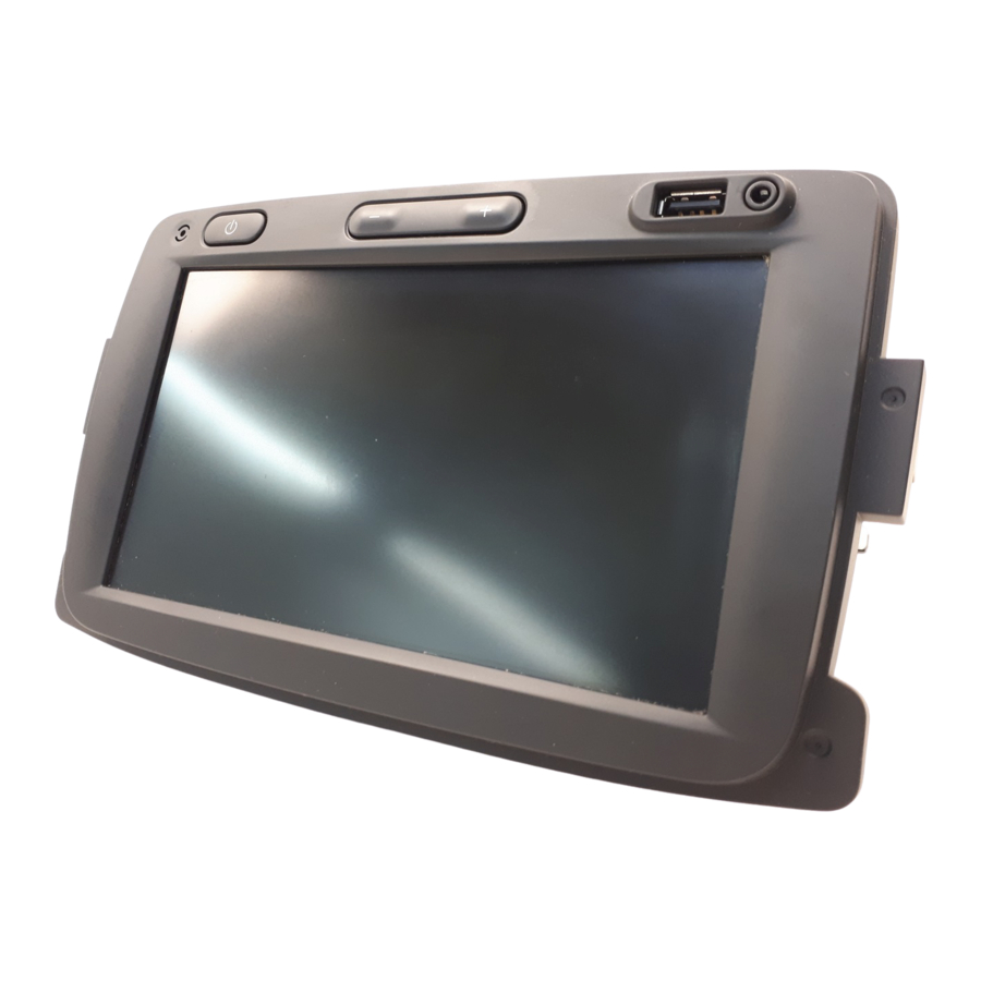
SPECIFICATION GENERAL Output Power ........................47 W x 4 CH (Max.) Power Source ............................. DC 13.8 V Speaker impedance ............................4 Ω Ground System .............................Negative Dimensions (W x H x D) ..................212.37 x 126.16 x 183.5 mm Net Weight ..............................1.4 kg DISPLAY LCD ......................... -
Page 6: Electrical Troubleshooting Guide
SECTION 2 ELECTRICAL ELECTRICAL TROUBLESHOOTING GUIDE 1. FRONT PART • FRONT_LCD ERROR LCD IS NOT OPERATED. All POWER CHECK CN2903(LCD_5 V 49, 48, 47PIN CHECK) AVDD(CN2905 8PIN), DVDD(CN2905 44PIN) POWER VGH(CN2905 10PIN), VGL(CN2905 9PIN), VCOM(CN2905 5PIN) CN2905(47, 48, 49, 50PIN CHECK) BACKLIGHT VLED+, VLED- CHECK VCOM(CN2905) CHECK... -
Page 7: Audio Part
2. AUDIO PART • AUDIO MICOM OPERATING ERROR POWER ERROR RESET (RECONNECT CN100 AND CN101) RESET? RESET IC(IC400) CHECK (R401) MICOM (IC401) INUPUT IC101 CHECK VOLTAGE(DC 3.3 V) (L402 CHECK) ACC_LEVEL_DETECT INPUT ACC CHECK (DC 3.3 V) OK? (MICOM PIN50) MICOM FLASH RE-DOWNLOAD (CN100) - Page 8 • AUDIO OUTPUT ERROR AUDIO OUTPUT ERROR CN100 CABLE CABLE CONNECTION & CONNECTION OK? CABLE CHECK DSP INPUT VOLTAGE(DC3.3 V) OK? LDO IC107 CHECK (IC300 PIN87(R341)) DSP OUTPUT OK? OUTPUT SHORT & DSP CLK (C317) BIAS 1.8 V, (R365(FL), R366(FR), CHECK R362(RL), R361(RR)) ∗...
- Page 9 • AUX SOURCE CHECKING [AUX source input checking] 1. Check front PCB TP2130 (Detect signal) → If it is failed, check AUX connector. 2. Check MAIN PCB. (Detect signal) 3. Check AUX Left, Right signal. (front : TP2168, TP2169 / MAIN : C319, C324) 4.
- Page 10 • USB, IPOD, BLUETOOTH SOURCE CHECKING [I2S data signal checking] 1. Check Main PCB R349. → If it is not failed, check DSP chip. 2. If R349 data is failed, a. Bluetooth : check Bluetooth chip (PCM, BT_Rx, BT_Tx), 40pin cable and CPU. b.
-
Page 11: Power Part
3. POWER PART • SET BOOTING ERROR BOOTING ERROR CN100 5PIN B+ CABLE CHECK 13.5 V? IC101 VOUT IC101 CHECK 3.3 V? IC104 3PIN IC104 CHECK 3.3 V? IC102 2PIN, 3PIN IC102 CHECK 3.3 V? IC108 4PIN IC108 CHECK 1.8 V? IC109 4PIN IC109 CHECK 1.1 V? - Page 12 • ACTIVE ANTENNA NG ACTIVE ANTENNA NG IC106 8PIN IC106 CHECK 5 V? D116 2PIN IC106 CHECK 12 V?
-
Page 13: Gps Part
4. GPS PART • SET BOOTING ERROR GPS RX ERROR IC1301_24PIN IC1301 CHECK 3.3 V HIGH? VDDC_8, 9, 17, 31PIN → 1.3 V? IC1301 PIN VDD_15, 25, 28, 29, 42, 50PIN → 3.3 V? IC1301 PIN IC1301- 49PIN PULSE XTAL-49PIN 26 MHz? UI CHECK... - Page 14 • GPS SATELLITE SIGNAL FIX ERROR GPS SATELLITE SIGNAL FIX ERROR IC1301_24PIN IC1301 CHECK 3.3 V HIGH? PIN49_XTAL_I (TCXO) X1301 3, 4PIN CHECK 26 MHz? PIN_6, 7 RTC XTAL X1300 1, 2PIN CHECK 32.768 kHz? UART GPS_TX IC1301- 21PIN CHECK NMEA DATA? CHECK GPS ANT...
-
Page 15: Connector Terminal Function
CONNECTOR TERMINAL FUNCTION 1. 24PIN SIGNAL CONNECTOR Signal Name Function Illumination Signal Wake-up Signal REAR GEAR Rear gear engaged MIC_SIG External microphone signal PWR_MIC External microphone supply PWR_CAM Rear camera power supply CAM_IN + Rear camera video signal + AUX2_IN + Line in mono + Line in detection INFO_AUX2_IN... - Page 16 2. 12PIN POWER / AUDIO CONNECTOR Signal Name Function HP AR G+ Left rear speaker + HP AV G+ Left front speaker + HP AV D+ Right front speaker + Radio Power Supply HP AR G- Left rear speaker - HP AV G- Left front speaker - HP AV D-...
- Page 17 2-12...
-
Page 18: Waveforms
WAVEFORMS 1. FRONT PART 2. AUDIO PART CN2903 31Pin DHSYNC CN2903 32Pin DVSYNC CN2903 2Pin DCLK CN2903 33Pin DTVDE DSP CLK (C317) POWER AMP_STBY (off → on) 3. MAIN PART [CPU] USBXI – X600, 12 MHz [CPU] XTI12 – X702, 12 MHz [CPU] XTI32 –... -
Page 19: Circuit Voltage Chart
CIRCUIT VOLTAGE CHART CN2903 CN2904 CN2905 Pin# Description Voltage Pin# Description Voltage Pin# Description Voltage Pin# Description Voltage Pin# Description Voltage Pin# Description Voltage DGND AUX_R MODEL_DETECT DCLK DGND DGND DGND AUX_L LCD_PWM DGND DGND DGND DITHB DGND AUX_DETECT AU_I2C_CLK0 VCOM_3.8 V 3.8 V DHSYNC... - Page 20 IC100 (MAX9938FELT+T) IC107 (BD7820FP) IC112 (AAT4610BIJS-1-T1) IC800 (TC1270ARVRCTR) IC1201 (LM20BIM7) EUSY0178502 EAN62046601 EAN62169401 EAN54854501 0IPRPNS034A Symbol Pin# Connection Symbol Pin# Connection Symbol Pin# Connection Symbol Pin# Connection Symbol Pin# Connection ANALOG 3.3 V DGND DGND 5.0 V 3.3 V /RST DGND DGND DGND...
- Page 21 IC102 (MAX15023ETG+T) IC200 (TEF7000HN/V2) IC1400 (LBMA-2C66C2-SA) EAN36285004 EAN60765801 EAT61553201 Symbol Pin# Connection Symbol Pin# Connection Symbol Pin# Connection Symbol Pin# Connection Symbol Pin# Connection Symbol Pin# Connection 0.6 V PGND2 DGND SWPORT1 ANALOG 3.3 V WXRFIN1 ADDRESS DGND DGND PCM_CLK 3.3 V PGOOD2 WXRFIN2...
- Page 22 IC1003 (MX29LV320ETTI-70G) 0IMMRMR027G Symbol Pin# Connection Symbol Pin# Connection Symbol Pin# Connection Symbol Pin# Connection Symbol Pin# Connection Symbol Pin# Connection DGND /RESET 3.3 V Q15/A-1 /WP/ACC 3.3 V DGND RY//BY /BYTE 3.3 V IC1300 (UBX-G6010-ST) EAN62215901 Symbol Pin# Connection Symbol Pin# Connection...
- Page 23 IC300 (SAF7741HV_N125) EAN60763802 Symbol Pin# Connection Symbol Pin# Connection Symbol Pin# Connection Symbol Pin# Connection Symbol Pin# Connection OSC_REF_N VDD_REG 3.3 V WS_IN2 T1E_WS DGND VSSS4 OSC_IN ANALOG FEBREG 1.8 V SD_IN2 T1E_SD_OUT DGND OSC_OUT ANALOG CONREG ANALOG BCK_IN3 T1E_SD_IN DGND DGND OSC_REF_P...
- Page 24 IC900 (V59C1G01168QBJ25AI) - 64Mx16 DDR2 IC901 (V59C1G01168QBJ25AI) - 64Mx16 DDR2 EAN61830801 (TOP VIEW: see balls through package) EAN61830801 (TOP VIEW: see balls through package) VSSQ /UDQS VDDQ VSSQ /UDQS VDDQ 1.8 V DGND DGND 1.8 V 1.8 V DGND DGND 1.8 V DQ14 VSSQ...
- Page 25 IC1002 (SDIN5D2-4G), 153 BALLS EAN62328201 (TOP VIEW: see balls through package) DAT0 DAT1 DAT2 DAT3 DAT4 DAT5 DAT6 DAT7 VDDi VSSQ VCCQ DGND DGND 3.3 V 3.3 V DGND 3.3 V DGND DGND 3.3 V RST_n DGND 3.3 V VCCQ 3.3 V VSSQ VCCQ...
- Page 26 IC600 (AU1320-667MTJ) EAN62229101 (TOP VIEW: see balls through package) GPIO[31]/ GPIO[7]/ GPIO[9]/ GPIO[4]/ BOOT[1] BOOT[2] TC[0] TC[2] CIM_D[9] CIM_D[5] CIM_D[1] CIM_D[0] TRST# LCD_D[2] LCD_D[3] LCD_D[6] LCD_D[11] LCD_LCLK LCD_PCLK LCD_ LCD_D[13] LCD_D[17] LCD_D[18] SD0_DAT5 SD0_DAT7 EXTCLK0 CLKIN 3.3 V DGND DGND DGND DGND DGND...
- Page 27 IC600 (AU1320-667MTJ) EAN62229101 (TOP VIEW: see balls through package) USB_ RCS[3]# EWAIT# RAD[11] RCS[2]# FTM_SEL# USBVDDX USBVDDX RKELVIN DGND 3.3 V DGND DGND DGND DGND DGND DGND DGND DGND DGND DGND DGND 3.3 V 3.3 V 3.3 V DGND DGND RCS[0]# RAD[10] RAD[13]...
-
Page 28: Block Diagrams
BLOCK DIAGRAMS 1. FUNCTION BLOCK DIAGRAM 2-33 2-34... -
Page 29: H/W Block Diagram
2. H/W BLOCK DIAGRAM 45 W × 4 Ch iNAND DDR2 DDR2 (4 GB) (128 MB) (128 MB) SDRAM eMMC IFAD Tuner 7" LCD Touch Module NAVI Audio MEDIA AUX In UART2 AU1320 (667 MHz) UART0 Debug D+/D- Protector Remote UART1 UART Controller... -
Page 30: S/W Block Diagram
3. S/W BLOCK DIAGRAM Application Application Application Firmware Firmware Firmware Radio System GUI Library App Main System Mgr BT App NAVI App Tuner Mgr Power Mgr RDS Mgr Functions Functions Functions Sound System Phone NAVI Multimedia Function Calling Audio Mgr NAVI Upgrade BT Mgr... -
Page 31: Front Block Diagram
4. FRONT BLOCK DIAGRAM TOUCH SCREEN IC UPD781845 MAX11803, MAXIM Flash 256 KB, RAM 16 KB AU1320 (NetLogic Microsystems) (power, volume) TOUCH PANEL TOUCH PANEL, TRULY 3.3 V BT MODULE TFT MODULE 1.5 V LBMA-2C66C2 3.3 V 7 inch (INNOLUX) LG INNOTEK LCD BLU (by LED’s) block... -
Page 32: Audio Block Diagram
5. AUDIO BLOCK DIAGRAM DSP 3 3 DiRaNa 1 8 _ . V TUNER Radio Audio (IC200) Antenna I2C (DICE) Power TEF7000HN NXP D D SP (IC110) (IC300) TDF8546, input SAF7741(DiRaNa) NXP input VDDX(3 3 V) VDDI (1 VDD ( . DDI (1.1 ) Bluetooth module... -
Page 33: Power Block Diagram
6. POWER BLOCK DIAGRAM GF1D NCV8664 MCU_3.3 V Battery 3.3 V LDO MCU 3.3 V, 0.5 A 14 V DDR_1.8 V RRH140P03TB DDR2*2EA 1.8 V, 0.6 A NCV5661 3.3 V 1.8 V CPU 1.8 V, 0.12 A VDDI 1.1 V CPU 1.1 V, 0.6 A NCV5661 VDDX... -
Page 34: Gps Block Diagram
7. GPS BLOCK DIAGRAM GPS ANTENNA 5 V ANT SAW Filter IC1300 – GPS CHIP IC600 – CPU FILTER UBX-G6010 UART GPIO GPS/GALILEO UART Integrated LNA Digital IF Filter Engine SRAM Power MGM AU1320 RF Front-End (NetLogic microsystems) ® ARM7TDM-S Backup RAM Fractional ROM Code... -
Page 35: Circuit Diagrams
CIRCUIT DIAGRAMS 1. FRONT CIRCUIT DIAGRAM When IC1400 is bad, BT do not operate. When IC2602 is bad, LCD do not operate. When IC2603 is bad, Touch do not operate. FRONT EAX63325601_16_1.6-SD 2012. 02. 03 2-47 2-48... -
Page 36: Main - Power + Amplifier Circuit Diagram
2. MAIN - POWER + AMPLIFIER CIRCUIT DIAGRAM When IC108 is bad, Set do not operate. When IC104 is bad, When IC101 is bad, When CN100 is bad, Set do not operate. Set do not operate. Set do not operate. When IC102 is bad, Set do not operate. -
Page 37: Main - Single Rf Tuner(Leaf Dice) Circuit Diagram
3. MAIN - SINGLE RF TUNER(LEAF DICE) CIRCUIT DIAGRAM MAIN - SINGLE RF TUNER(LEAF DICE) EAX64206903_0_1.0-SD(#2) 2012. 02. 03 2-51 2-52... -
Page 38: Main - Dsp(Dirana2) Circuit Diagram
4. MAIN - DSP(DiRaNa2) CIRCUIT DIAGRAM MAIN - DSP (DiRaNa2) EAX64206903_0_1.0-SD(#3) 2012. 02. 03 2-53 2-54... -
Page 39: Main - Micom + Can Circuit Diagram
5. MAIN - MICOM + CAN CIRCUIT DIAGRAM MAIN - MICOM+CAN EAX64206903_0_1.0-SD(#4) 2012. 02. 03 2-55 2-56... -
Page 40: Main - Dab Circuit Diagram
6. MAIN - DAB CIRCUIT DIAGRAM MAIN - EAX64206903_0_1.0-SD(#5) 2012. 02. 03 2-57 2-58... -
Page 41: Main - Au1320 Lcd & Usb & Uart Circuit Diagram
7. MAIN - AU1320 LCD & USB & UART CIRCUIT DIAGRAM MAIN - AU1320 LCD & USB & UART EAX64206903_0_1.0-SD(#6) 2012. 02. 03 2-59 2-60... -
Page 42: Main - Au1320 Bus & Psc Circuit Diagram
8. MAIN - AU1320 BUS & PSC CIRCUIT DIAGRAM MAIN - AU1320 BUS & PSC EAX64206903_0_1.0-SD(#7) 2012. 02. 03 2-61 2-62... -
Page 43: Main - Au1320 Vdd & Boot & Reset / Ipod Cp Circuit Diagram
9. MAIN - AU1320 VDD & BOOT & RESET / IPOD CP CIRCUIT DIAGRAM MAIN - AU1320 VDD & BOOT & RESET / IPOD CP EAX64206903_0_1.0-SD(#8) 2012. 02. 03 2-63 2-64... -
Page 44: Main - Ddr2 Sdram Circuit Diagram
10. MAIN - DDR2 SDRAM CIRCUIT DIAGRAM MAIN - DDR2 SDRAM EAX64206903_0_1.0-SD(#9) 2012. 02. 03 2-65 2-66... -
Page 45: Main - Nor Flash & I-Nand Circuit Diagram
11. MAIN - NOR FLASH & i-NAND CIRCUIT DIAGRAM MAIN - NOR FLASH & i-NAND EAX64206903_0_1.0-SD(#10) 2012. 02. 03 2-67 2-68... -
Page 46: Main - Video Decoder & Usb Circuit Diagram
12. MAIN - VIDEO DECODER & USB CIRCUIT DIAGRAM MAIN - VIDEO DECODER & USB EAX64206903_0_1.0-SD(#11) 2012. 02. 03 2-69 2-70... -
Page 47: Main - Connector & Debug Circuit Diagram
13. MAIN - CONNECTOR & DEBUG CIRCUIT DIAGRAM MAIN - CONNECTOR & DEBUG EAX64206903_0_1.0-SD(#12) 2012. 02. 03 2-71 2-72... -
Page 48: Main - Gps Circuit Diagram
14. MAIN - GPS CIRCUIT DIAGRAM MAIN - GPS EAX64206903_0_1.0-SD(#13) 2012. 02. 03 2-73 2-74... -
Page 49: Printed Circuit Board Diagrams
PRINTED CIRCUIT BOARD DIAGRAMS 1. FRONT P.C.BOARD (TOP VIEW) 2-75 2-76... - Page 50 (BOTTOM VIEW) 2-77 2-78...
-
Page 51: Main P.c.board
2. MAIN P.C.BOARD (TOP VIEW) 2-79 2-80... - Page 52 (BOTTOM VIEW) 2-81 2-82...
- Page 53 2-83 2-84...
-
Page 54: Exploded View
SECTION 3 EXPLODED VIEW 1. CABINET AND MAIN FRAME SECTION CABLE2 FRONT CABLE1 MIC1 MAIN...
Need help?
Do you have a question about the LAN5200WR1 and is the answer not in the manual?
Questions and answers