Yamaha DSP-A595a Service Manual
Hide thumbs
Also See for DSP-A595a:
- Owner's manual (53 pages) ,
- Owner's manual (60 pages) ,
- Service manual (44 pages)
Table of Contents
Advertisement
DSP-A595a
CONTENTS
To Service Personnel ........................................... 1
Remote Control Panels ....................................... 1
Rear Panels ............................................................... 2
Specifications ....................................................... 3~4
INTERNAL VIEW ............................................................ 5
Disassembly Procedures .................................... 5
Self Diagnosis Function ................................ 6~17
Factory Preset ...................................................... 18
1 0 0 6 7 8
SERVICE MANUAL
IMPORTANT NOTICE
This manual has been provided for the use of authorized YAMAHA Retailers and their service personnel.
It has been assumed that basic service procedures inherent to the industry, and more specifically YAMAHA
Products, are already known and understood by the users, and have therefore not been restated.
WARNING:
Failure to follow appropriate service and safety procedures when servicing this product
may result in personal injury, destruction of expensive components, and failure of the
product to perform as specified. For these reasons, we advise all YAMAHA product
owners that any service required should be performed by an authorized YAMAHA
Retailer or the appointed service representative.
IMPORTANT:
The presentation or sale of this manual to any individual of firm does not constitute
authorization, certification or recognition of any applicable technical capabilities,
or establish a principle-agent relationship of any form.
The data provided is believed to be accurate and applicable to the unit(s) indicated on the cover. The research,
engineering, and service departments of YAMAHA are continually striving to improve YAMAHA products.
Modifications are, therefore, inevitable and specifications are subject to change without notice or obligation
to retrofit. Should any discrepancy appear to exist, please contact the distributor's Service Division.
WARNING:
Static discharges can destroy expensive components. Discharge any static electricity
your body may have accumulated by grounding yourself to the ground buss in the unit
(heavy gauge black wires connect to this buss).
IMPORTANT:
Turn the unit OFF during disassembly and part replacement. Recheck all work before
you apply power to the unit.
Amp Adjustment ..................................................... 19
Ic Data .................................................................. 20~30
Display Data ........................................................... 31
Block Diagram .................................................. 32~33
Printed Circuit Board ................................... 34~47
Schematic Diagram ......................................... 48~53
Parts List ............................................................ 54~67
REMOTE CONTROL TRANSMITTER ......................... 68
AV AMPLIFIER
Advertisement
Table of Contents

Related Manuals for Yamaha DSP-A595a


Summary of Contents for Yamaha DSP-A595a
- Page 1 SERVICE MANUAL IMPORTANT NOTICE This manual has been provided for the use of authorized YAMAHA Retailers and their service personnel. It has been assumed that basic service procedures inherent to the industry, and more specifically YAMAHA Products, are already known and understood by the users, and have therefore not been restated.
-
Page 2: To Service Personnel
DSP-A595a TO SERVICE PERSONNEL 1. Critical Components information. Components having special characteristics are marked and must be replaced with parts having specifications equal to those originally AC LEAKAGE installed. WALL EQUIPMENT TESTER OR 2. Leakage Current Measurement (For 120V Model only). -
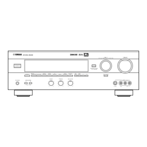
Page 3: Rear Panels
DSP-A595a REAR PANELS R model T model B model G model... -
Page 4: Specifications
DSP-A595a SPECIFICATIONS Residual Noise(IHF-A Network) AUDIO SECTION MAIN L/R, SP OUT 150µV Minimum RMS Output Power Per Channel Channel Separation(Vol. –30dB, EFFECT OFF) (Power Amp. Section) PHONO, Input shorted, 1kHz/10kHz 60dB/55dB MAIN L/R, REAR L/R CD etc, Input 5.1kΩ terminated, 1kHz/10kHz 20Hz to 20kHz, 0.04% THD, 8Ω... - Page 5 DSP-A595a DIMENSIONS WARNING Do not change the IMPEDANCE SELECTOR switch setting while the power to this unit is on, otherwise this unit may be damaged. IMPEDANCE SELECTOR Manufactured under license from Digital Theater Systems, Inc. US Pat. No. 5,451,942 and other wirld- wide patents issued and pending.
-
Page 6: Internal View
DSP-A595a INTERNAL VIEW 1 2 3 4 5 6 1 POWER TRANSFORMER 2 P.C.B. MAIN (3) 3 P.C.B. OPERATION (7) (R, T models only) 4 P.C.B. OPERATION (3) 5 P.C.B. MAIN (4) 6 P.C.B. MAIN (8) 7 P.C.B. OPERATION (6) 8 P.C.B. -
Page 7: Self Diagnosis Function
SELF DIAGNOSIS FUNCTION 1. PURPOSE AND OPERATION The DSP-A595a has a Self Diagnosis Function to locate a faulty part, if any, by inspecting and taking measurements. There are 11 main items in the diagnostic menu and some of them have sub-menu items as listed below. - Page 8 DSP-A595a 2. BEGINNING AND CANCELLATION (1) STARTING UP THE FUNCTION AND THE DISPLAY After starting up, menu No. 1 is selected. A. How to start diagnostic program Using the front panel keys of the main unit. Plug in the AC power cord , and, with Power OFF, hold down the "INPUT MODE" and "+" keys simultaneously (Step 1), and then press the "STANDBY/ON"...
- Page 9 DSP-A595a FL display at start-up of diagnostic program When the diagnostic program has started, the history (*2) of the protection function (*1) is displayed. If the protection function has been activated in the past, the type and voltage value are displayed. After a few seconds the diagnosis function menu will appear.
- Page 10 DSP-A595a 3. OPERATION AND DISPLAY WHEN STARTING DIAGNOSIS FUNCTION (1) Selection of diagnostic menu The diagnostic menu and the sub-menu can be selected by using the front panel keys of the main unit or the remote control unit. Selection by using the front panel keys The main menu can be changed cyclically by using the "TV SPORTS"...
- Page 11 DSP-A595a 4. CONTENTS OF DIAGNOSIS FUNCTION This section describes the contents of the self diagnosis function in detail. No.1 ANALOG THROUGH The input is fixed to analog (A/D). There are two submenus. 1 DVD/LD MAIN BYPAS 1. MAIN BYPASS The MAIN L/R signals bypass the analog circuits to be output.
- Page 12 DSP-A595a No.2 DSP THROUGH The input is automatically discriminated by signal detection and switched with priorities AC-3 (DOLBY DIGITAL)>DTS Digital Surround>Audio>analog. There are the following three submenus. 2 DVD/LD YSS918SRAM 1. YSS918-SRAM MAIN L/R are input to the DSP via AC3D2av, pass through SRAM, and are then output to all channels without being processed.
- Page 13 DSP-A595a No.3 AC-3/DTS THROUGH The input is digital signal only. AC-3 (DOLBY DIGITAL) or DTS Digital Surround decoding operation is executed, according to the input source. bit 0 bit 7 3 DVD/LD 3T00000001 1. STATUS(BINARY FORM) AC-3 (DOLBY DIGITAL) decoded signals are output to each channel via AC3D2av.
- Page 14 DSP-A595a No.5 SPEAKERS SET The input is automatically discriminated by AC-3(DOLBY DIGITAL)>DTS Digital Surround>PCM Audio>analog. There are the following 9 submenu items: The signal from the DSP block is normally in the effect off status for menu items 1-4. For other menu items, the same signal as in 2. DSP THROUGH: YSS918 menu is output.
- Page 15 DSP-A595a No.6 DISPLAY CHECK Check program for FL display. The display status will change as follows with submenu operation. The signal is processed with EFFECT OFF. 6 DVD/LD DISP CHECK Initial display All segments turn off All segments turn on...
- Page 16 DSP-A595a No.9 AD DATA CHECK The A/D conversion values of the main CPU which detects key scan, protection, etc. are displayed in % (100%: 5V). All signal processing before this menu is executed will be held. The keys on the main unit cannot be operated to detect the values of all keys in the K1/K2/K3/K4 and SI.
- Page 17 DSP-A595a No.10 STATUS FROM DSP MICOM The status data from the DSP microprocessor is sequentially displayed in a hexadecimal number. All signal processing before this menu is executed will be held. STATUS 1st 2nd 3rd 4th 10 DVD/LD 0 00000000...
- Page 18 DSP-A595a No.11 CPU VERSION/CHECK SUM/PORT INFO/EXIT DIAG The check sum, version and port setting of main CPU/DSP CPU are displayed. The signal is EFFECT OFF. Operating the submenu will finish self-diagnosis, and ordinary operation mode will be restored. The suffix letter ("B" in the following) of version indication is for compatibility of communications between the main and DSP microprocessors.
-
Page 19: Factory Preset
DSP-A595a FACTORY PRESET All of the system settings are initially set from the factory as follows. INPUT (VIDEO) DVD/LD (DVD/LD) EFFECT LEVEL EFFECT CHANNEL PRESET VALUE CENTER 0 dB RIGHT SURROUND 0 dB LEFT SURROUND 0 dB SUBWOOFER 0 dB... -
Page 20: Amp Adjustment
DSP-A595a AMP ADJUSTMENT Confirmation of Idling Current of Main Amplifier • Right after power is turned on, confirm that the voltage across the terminals of R688(Main Lch),R690(Main Rch), R692(Center), R694(Rear Lch), R696(Rear Rch) are between 0.1mVand 5.0mV. • If it exceeds 5.0mV, open (cut off) R571 (Main Lch), R577 (Main Rch), R589 (Center), R595 (Rear Lch), R583 (Rear Rch) and reconfirm the voltage again. - Page 21 DSP-A595a IC DATA IC800 : LC876564A-5M19 µ 8 bit Main -COM S48/PG0 S19/PC3 S49/PG1 S18/PC2 S50/PG2 S17/PC1 S51/PG3 S16/PC0 VDD3 S15/T15 S14/T14 S13/T13 VSS2 S12/T12 VDD2 S11/T11 TOP VIEW S10/T10 S9/T9 S8/T8 S7/T7 P10/SO0 S6/T6 P11/SI0 S5/T5 P12/SCK0 S4/T4 P13/SO1...
- Page 22 DSP-A595a IC800 : LC876564A-5M19 µ 8 bit Main -COM Port Function Port Function Name Name FLA-CLK I/O Flash clock 26 P70/INT0 I Power down detect FLA-I/O I/O Flash input/output 27 P71/INT1 O Full mute (L : ON) FLA-SEL I/O Flash select...
- Page 23 DSP-A595a IC800 : LC876564A-5M19 µ 8 bit Main -COM Port Function Port Function Name Name 76 S43/PF3 POWER-RY O Power relay 52 S20/PC4 O FL Segment 5 77 S44/PF4 –10dB O –10 dB select (L : –10dB) 53 S21/PC5 O FL Segment 6...
- Page 24 DSP-A595a IC14 : LC875164A-5K20 µ 8 bit Sub -COM PWM1 SI2P3 SCK2 P17/PWM P16/PWL VSS3 P15/SCK1 VDD3 P14/SI1 P13/SO1 TOP VIEW P12/SCK0 P11/SI0 P10/SOO P87/AN7 P86/AN6 INTERRUPT CONTROL STANDBY /RES CONTROL CLOCK GENE- RATOR Xtal SERIAL I/O 0 BUS INTERFACE...
- Page 25 DSP-A595a IC14 : LC875164A-5K20 µ 8 bit Sub -COM Port Function Port Function Name Name I Receive data from DIR2 PWM0 OL Unconnected /ICDI O Initial clear for DIR2 VDD2 VDD2 +5V +5V power supply /KM1 O Switching DIR2 forced (analog) mode...
- Page 26 DSP-A595a IC3 : YM3436DK (DIR2) Digital Format Interface Receiver 24 26 28 25 17 15 14 13 12 31 EXTW DOM0 SYSTEM CLOCK EXTW DOM1 TIMING DDIN DIM0 SYNC GENERATOR DIM1 DDIN TOP VIEW TST2 DATA CLOCK EIAJ (AES/EBU) CONTROLLER...
- Page 27 DSP-A595a IC4 : YSS918D-F (AC3D2av) DSP + AC-3 (Digital Dolby)/Pro Logic/DTS Digital Surround Decoder PVSS SDWCK0 SDWCK1 SDBCK0 SDBCK1 SDIA0 SDOB0 SDIA1 SDOB1 RAMA1 SDOB2 RAMA0 RAMA7 RAMWEN RAMA8 RAMOEN RAMA9 TOP VIEW VDD2 IPORT7 OPORT7 IPORT6 OPORT6 IPORT5 OPORT5...
- Page 28 DSP-A595a IC4 : YSS918D-F (AC3D2av) DSP + AC-3 (Digital Dolby)/Pro Logic/DTS Digital Surround Decoder Name Function VDD1 +5V power supply RAMCEN RAM chip enable output terminal (normally unconnected) RAMA16 RAM address output terminal 16, connected to external 1M SRAM address...
- Page 29 DSP-A595a IC4 : YSS918D-F (AC3D2av) DSP + AC-3 (Digital Dolby)/Pro Logic/DTS Digital Surround Decoder Name Function VDD2 +3V power supply NONPCM non-PCM data output terminal, non-PCM data detect CRC output terminal (normally unconnected) MUTE Mute output terminal, output data mute detect...
- Page 30 DSP-A595a IC5 : M5M51288BKJ-20LTEL (1M SRAM) 131072-word x 8 bit High Speed Static RAM 131072-word x 8 bit MEMORY ARRAY (512-row X 2048-column) 2048 TOP VIEW COLUMN I/O COLUMN ADDRESS /CE1 DECODER COLUMN INPUT BUFFER /CE1 CHIP SELECT WRITE CONTROL...
-
Page 31: Display Data
DSP-A595a DISPLAY DATA IC6 : AK4526A-VQ (CODEC AD/DA) 20 bit 6 channel A/D, D/A Converter V800 : 16-BT-59GK (V2421800) LIN+ Audio PATTERN AREA LIN– Clock Gen. RIN+ MCLK SDOS VREFL RIN– LRCK OCKS RIN+ BICK • PIN CONNECTION RIN– LOUT1... -
Page 32: Block Diagram
DSP-A595a BLOCK DIAGRAM PHONES MAIN SELECTOR MAIN POWER AMP VR401 LEVEL IC10A IC102 IC103 Q506,511,512, IC103 IC351 IC401A IC802A 521,529,Q527A/C IC108B INPUT MAIN COAXIAL SELECTOR IC352 H,P,F Q810 Q501 DVD/LD OPTICAL IC103 TONE IC10B IC103 CONTROL TV/DBS OPTICAL RY501 OPTICAL SIGNAL... -
Page 33: Printed Circuit Board
DSP-A595a PRINTED CIRCUIT BOARD (Foil side) P. C. B. DSP P. C. B. DSP TO: INPUT (1) TO: INPUT (3) TO: INPUT (1) LC875164A-5K20 HD74HC02FP YSS918D-F YM3436DK AK4526A-VQ AK4320 Semiconductor Location Point Point Pin 13 of IC14 Ref. No. Location Ref. - Page 34 DSP-A595a PRINTED CIRCUIT BOARD (Foil side) P. C. B. OPERATION (1) Semiconductor Location Ref. No. Location D800 D801 D802 D803 D805 EFFECT /DTS MOVIE MONO ROCK CONCERT D806 SURROUND ENHANCED THEATER MOVIE SPORTS DISCO CONCERT HALL D807 D808 D809 D811...
- Page 35 DSP-A595a P. C. B. OPERATION (6) PRINTED CIRCUIT BOARD (Foil side) P. C. B. OPERATION (5) • J, R and T models SWITCHED 100W MAX. TOTAL P. C. B. OPERATION (3) AC OUTLETS R, T models only J, R and T Models Semiconductor Location Ref.
- Page 36 DSP-A595a PRINTED CIRCUIT BOARD (Foil side) P. C. B. MAIN (1) B, G models only NFRL NFRR –B B, G only SPRY PRV1 B, G only W803 W504 TO: MAIN (3) TO: OPERATION (1) W761 W815 TO: MAIN (4) TO: OPERATION (3) P.
- Page 37 DSP-A595a PRINTED CIRCUIT BOARD (Foil side) P. C. B. MAIN (7) P. C. B. MAIN (6) P. C. B. MAIN (3) P. C. B. MAIN (4) TO: INPUT (1) TO: MAIN (1) W761 TO: MAIN (1) OPERATION (5) W504 –B2...
- Page 38 DSP-A595a PRINTED CIRCUIT BOARD (Foil side) Semiconductor Location Ref. No. P. C. B. INPUT (1) Location D101 D102 D103 D104 TO: DSP TO: DSP IC101 IC102 IC103 IC104 IC106 IC107 IC108 IC109 B, G only IC110 IC111 IC112 IC113 Q101...
- Page 39 DSP-A595a PRINTED CIRCUIT BOARD (Foil side) P. C. B. INPUT (3) P. C. B. INPUT (4) P. C. B. VIDEO TO: INPUT (1) W102 –12 +12A LFEO INPUT (1) W101 TO: DSP +12A TO: INPUT (1) /VCR VSEL1 VSEL0 DSIG...
-
Page 40: Schematic Diagram
DSP-A595a SCHEMATIC DIAGRAM (VIDEO) S-VIDEO SELECTOR VIDEO SELECTOR & AMP & AMP VIDEO SIGNAL DVD/LD VIDEO SIGNAL TO INPUT (1) CB101 page E-50/J-48 DVD/LD TV/DBS VIDEO TO OPE (2) S VIDEO CB807 page E-52/J-50 11.6 MONITOR MONITOR VIDEO PIN CONNECTION DIAGRAM OF IC301~305 : LA7956 TRANSISTORS AND IC’s. - Page 41 DSP-A595a SCHEMATIC DIAGRAM (INPUT) TO OPE(4) CB802 VOLUME AMP FRONT L REAR L page E-52/J-50 H-4 TO DSP CB6 page E-53/J-51 N-4 MAIN L MAIN L MAIN L MAIN L (DSP) (DSP) 11.7 CENTER PHONO(MM) CENTER/SUB WOOFER/FRONT/REAR AMP CENTER EQ AMP 23.3...
- Page 42 DSP-A595a SCHEMATIC DIAGRAM (MAIN) REGULATOR MAIN (1),(2),(5),(6) MAIN (3),(4),(7),(8) MAIN POWER AMP 29.4 12.8 43.5 13.4 43.4 43.5(30.2) OUTPUT MAIN POWERAMP 43.5(30.2) MAIN L 43.3 C751 752 8200/56 8200/56 8200/56 (V317930) (VV95180) (VV95180) -0.5 :NOT USED MAIN MUTE -1.1 -11.6 SPEAKERS -41.7...
- Page 43 DSP-A595a SCHEMATIC DIAGRAM (OPERATION) S VIDEO IC801, 802 : NJM2068LD Dual OP-Amp VIDEO – – 2 3 4 5 6 • IC800: LC876564A-5M19→See page E-20/J-18~E-22/J-20 AUDIO -22.7 -29.7 OPE(2),(3),(4) TONE CONTROL -11.7 NJM2068LD 11.8 11.8 -19 .6 -11.7 SYSTEM & DSP -8.9...
- Page 44 DSP-A595a SCHEMATIC DIAGRAM (DSP) TO INPUT(3) CB354 page E-50/J-48 N-8 AK4526A-VQ AK4526VQ DIGITAL Point Pin 13 of IC3 V : 2V/div H : 50nsec/div AC range 1 : 1probe L.P.F 3. 1 2. 4 DSP + DOLBY DIGITAL/ 2. 4 2.
-
Page 45: Parts List
DSP-A595a WARNING PARTS LIST Components having special characteristics are marked and must be replaced with parts having specifications equal to those originally installed. ELECTRICAL PARTS Carbon resistors (1/6W or 1/4W) are not included in the ELECTRICAL PARTS List. For the part Nos. of the carbon resistores, refer to the last page. - Page 46 DSP-A595a P. C. B. DSP Schm Schm PART NO. Description PART NO. Description V4035900 P.C.B. UR818330 C.EL 330uF 6.3V VQ044200 CN.BS.PIN UB245100 C.CE.M.CHP 0.1uF VQ044500 CN.BS.PIN UR818330 C.EL 330uF 6.3V VQ044600 CN.BS.PIN UB245100 C.CE.M.CHP 0.1uF UB245100 C.CE.M.CHP 0.1uF UB245100 C.CE.M.CHP 0.1uF UB052100 C.CE.M.CHP 100pF...
- Page 47 DSP-A595a P. C. B. DSP & P. C. B. VIDEO Schm Schm PART NO. Description PART NO. Description C122 UA952100 C.MYLAR 100pF IC14 XV260E00 IC LC875164A-5K20 CPU C123 UR837220 C.EL 22uF IC15 XU965A00 IC uPC29M33T-E1 3.3V C124 UR847100 C.EL 10uF VV655300 TR.DGT...
- Page 48 DSP-A595a P. C. B. VIDEO & P. C. B. MAIN Schm Schm PART NO. Description PART NO. Description C320 VF467000 C.CE.TUBLR 1000pF C507 UR837470 C.EL 47uF C321 UR829100 C.EL 1000uF C508 UR847100 C.EL 10uF C322 UR837100 C.EL 10uF C509 UR847100 C.EL...
- Page 49 DSP-A595a P. C. B. MAIN Schm Schm PART NO. Description PART NO. Description C555 VR325000 C.MYLAR 100pF 100V C765 UA954680 C.MYLAR 0.068uF 50V(BG) C556 UR867470 C.EL 47uF C766 UA952220 C.MYLAR 220pF C557 VR325000 C.MYLAR 100pF 100V D501 VM975700 DIODE.ZENR HZS12C2TD 12V C558 UA954680 C.MYLAR...
- Page 50 DSP-A595a P. C. B. MAIN Schm Schm PART NO. Description PART NO. Description Q523 iC174020 2SC1740S R,S R587 HV756270 R.CAR.FP 2.7KΩ 1/4W Q524 iC174020 2SC1740S R,S R589 HV755820 R.CAR.FP 820Ω 1/4W Q525 iC174020 2SC1740S R,S R590 HV756100 R.CAR.FP 1KΩ 1/4W...
- Page 51 DSP-A595a P. C. B. MAIN & P. C. B. INPUT Schm Schm PART NO. Description PART NO. Description RY503 VK438300 RELAY DH24D2-OT/M2 C124 UA655220 C.MYLAR 0.22uF SW711 VV523900 SW.PUSH PBS-YM-001 C125 VF467300 C.CE.TUBLR 0.01uF SW761 VZ361100 SW.SLIDE SL13B-022-AMC1 C126 UR866220 C.EL 2.2uF...
- Page 52 DSP-A595a P. C. B. INPUT Schm Schm PART NO. Description PART NO. Description C180 UR837470 C.EL 47uF C417 UR838100 C.EL 100uF C181 UR837470 C.EL 47uF C418 UR838100 C.EL 100uF C182 UR837470 C.EL 47uF C419 VG277000 C.CE.TUBLR 33pF 50V(BG) C183 UR847470 C.EL...
- Page 53 DSP-A595a P. C. B. INPUT & P. C. B. OPERATION Schm Schm PART NO. Description PART NO. Description PJ352 VY667700 JACK.PIN C804 UR866100 C.EL Q101 iC287820 2SC2878 A,B C805 VJ599100 C.CE.TUBLR 0.1uF R141 HV755100 R.CAR.FP 100Ω 1/4W C806 UR819100 C.EL 1000uF 6.3V...
- Page 54 DSP-A595a P. C. B. OPERATION Schm Schm PART NO. Description PART NO. Description D811 VD631600 DIODE 1SS133,176,HSS104 T800 XT331A00 TRANS.PWR (RT) D812 VM974400 DIODE.ZENR HZS6B2TD 6.0V(RT) TE800 V4746500 OUTLET.AC 3P(RT) D812 VM974600 DIODE.ZENR HZS7A2TD 7.0V(BG) TE800 VU543300 OUTLET.AC 1P(B) D813 VM974500 DIODE.ZENR HZS6C2TD 6.0V...
- Page 55 DSP-A595a Chip Resistors Schm PART NO. Description RD250000 R.CAR.CHP 0Ω 1/10W RD254470 R.CAR.CHP 47Ω 1/10W RD255100 R.CAR.CHP 100Ω 1/10W RD255330 R.CAR.CHP 330Ω 1/10W RD256100 R.CAR.CHP 1KΩ 1/10W RD256120 R.CAR.CHP 1.2KΩ 1/10W RD256150 R.CAR.CHP 1.5KΩ 1/10W RD256220 R.CAR.CHP 2.2KΩ 1/10W RD256330 R.CAR.CHP 3.3KΩ...
-
Page 56: Exploded View
DSP-A595a EXPLODED VIEW 2-23 2-11 2-23 2-24 2-12 2-21 Ass'y (R,T only) Ass'y Ass'y (B,G only) 2-18 Ass'y 2-22 2-21 2-17 2-21 2-15 3-14 3-11 (R,T only) 3-13 3-12 3-20 B model (G only) G model (G only) 200-1... -
Page 57: Remote Control Transmitter
DSP-A595a MECHANICAL PARTS Ref. Ref. PART NO. Description Remarks Markets PART NO. Description Remarks Markets 1- 1 V3827000 FRONT PANEL V2461100 SHIELD CASE 1- 1 V3827100 FRONT PANEL VZ332800 SHIELD CASE COVER 1- 4 V2468600 ESCUTCHOEN V2460900 FRAME 2- 1 V4036800 P.C.B. - Page 58 DSP-A595a Parts List for Carbon Resistors REMOTE CONTROL TRANSMITTER (RAV174 or RAV175) SCHEMATIC DIAGRAM • R and T models → RAV174 Value 1/4W Type Part No. 1/6W Type Part No. Value 1/4W Type Part No. 1/6W Type Part No. • B and G models → RAV175 K10 K20 K30 1.0 Ω...