Table of Contents
Advertisement
Quick Links
Download this manual
See also:
Instruction Manual
SERVICE MANUAL
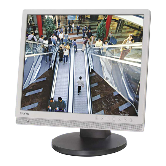
Color LCD monitor
CONTENTS
SPECIFICATIONS..................................... 4
1. DISASSEMBLY ..................................... 5
2. ADJUSTMENT ......................................6
3. PARTS LIST .........................................8
RoHS
This product does not contain any hazardous substances prohibited by the RoHS Directive.
WARNING
You are requested to use RoHS compliant parts for maintenance or repair.
You are requested to use lead-free solder.
(This product has been manufactured using lead-free solder. Be sure to follow the warning given on page 3 when carrying
out repair work.)
NOTE: 1. Parts order must contain model number, part number, and description.
2. Substitute parts may be supplied as the service parts.
3. N.S.P. : Not available as service parts.
Design and specifications are subject to change without notice.
L8MAP/XE, US (R)
FILE NO.
VMC-L2619P
(Product Code : 114 956 09)
(Europe, U.K., PAL General)
VMC-L2619
(Product Code : 114 956 11)
(U.S.A., Canada, NTSC General)
REFERENCE No.SM5310788
Advertisement
Chapters
Table of Contents

Related Manuals for Sanyo VMC-L2619


Summary of Contents for Sanyo VMC-L2619
-
Page 1: Table Of Contents
FILE NO. SERVICE MANUAL Color LCD monitor VMC-L2619P (Product Code : 114 956 09) (Europe, U.K., PAL General) VMC-L2619 (Product Code : 114 956 11) (U.S.A., Canada, NTSC General) CONTENTS SPECIFICATIONS........4 1. DISASSEMBLY ........5 2. ADJUSTMENT ........6 3. PARTS LIST .........8 CIRCUIT DIAGRAMS &... -
Page 2: Safety Precautions
SAFETY PRECAUTIONS WARNING: Service should not be attempted by anyone unfamiliar with the necessary precautions for this recording or playback equipment. The following precautions are necessary during servicing: 1. Many electrical and mechanical parts in this recorder have 3. Before returning the set to the customer, always perform special safety-related characteristics for providing protec- an AC leakage current check on the exposed metallic parts tion against shock, fire and other hazards. - Page 3 WARNING Do not use solder containing lead. Note: This product has been manufactured using lead-free If replacing existing solder containing lead with lead-free solder in order to help preserve the environment. solder in the soldered parts of products that have been manufactured up until now, remove all of the existing solder Because of this, be sure to use lead-free solder when at those parts before applying the lead-free solder.
-
Page 4: Specifications
SPECIFICATIONS Display type : SXGA a-Si TFT LCD Color system : PAL/NTSC (Automatic detection) LCD display : 19” active matrix TFT LCD panel Viewable size (H x V) : 376 x 301 mm/14.8 x 11.9 in. (4:3) Pixel pitch (H x V) : 0.294 x 0.294 mm/0.012 x 0.012 in. Horizontal resolution : 1280 x 1024, PAL: 620 NTSC: 600 TV lines (Y/C input mode) Viewing angle degree : Left/Right/Up/Down: 80°... -
Page 5: Disassembly
1. DISASSEMBLY 1-1. DISASSEMBLY 1. Remove the two screws 4 x 10. 13. Remove the screw 3 x 8. 2. Remove the ass’y stand P. 14. Remove the ass’y IR board. 15. Remove the ass’y FUNCTION board. 16. Cover front. 3. -
Page 6: Adjustment
2. ADJUSTMENT This section describes to adjust LCD monitor after replacing FLASH, Main board or Panel. 2-1. Program Upgrade Change MICOM If the similer happenings occur, FLASH can be changed EX1) When screen appears but remote control and function key aren’t working EX2) When LED is on but the screen doesn’t appear EX3) After mass production, when the micom program version is up-graded *FLASH replacement can be done when Service Bulletin issue is in practice. - Page 7 2-2. Factory Mode Adjustments Factory Mode Admission 2-2-1. Power on MUTE Service Mode Menu 2-2-2. Calibration Option Table (Service) Adjust W/B Movie 1. AV calibration 1. Ready 1. V Mute time 1. WB movie 2. COMP calibration 2. Inch option 2.
-
Page 8: Parts List
ASSY STAND P TFBN63-03284A COVER-JACK TFAB94-00152B MAIN PCB TFBN44-00137D IP BOARD ACCESSORIES & PACKING MATERIALS TFAB96-01032A ASSY ACCESSORY (MANUAL USE) TFAB59-00030A REMOCON TFBN83-01230F CKD-POWER CORD,VMC-L2619P ONLY TFBN83-01230G CKD-POWER CORD,VMC-L2619 ONLY TFBN83-01230J CKD-SIGNAL CABLE TFBN69-01783A CUSHION-SET TFBN69-01795C BOX-SET TF6902-001067 BAG PE... - Page 9 CABINET & CHASSIS PARTS N.S.P. N.S.P. N.S.P. L8MAQ-US_CAB ACCESSORIES & PACKING MATERIALS...
-
Page 10: Circuit Diagrams & Printed Wiring Boards
CIRCUIT DIAGRAMS & PRINTED WIRING BOARDS TABLE OF CONTENTS OVERALL WIRING, BLOCK DIAGRAMS & CIRCUIT DIAGRAMS Page OVERALL WIRING OVERALL CIRCUIT BLOCK DIAGRAM MAIN BOARD SIGNAL INPUT MAIN BOARD TV PROCESSOR MAIN BOARD SCALAR & MEMORY MAIN BOARD POWER REGULATOR MAIN BOARD SOUND FUNCTION BOARD KEY SWITCH IR BOARD IR RECEIVER... - Page 11 NOTES: 1. All resistance values in "OHMS" unless otherwise noted. (K=1,000 ; M=1,000,000) 2. All capacitance values in "µF" unless otherwise noted. p=pico farad ; n=nano farad ; µ ,u or U=micro farad 3. All inductance values in "µH" unless otherwise noted. µ...
-
Page 12: Overall Circuit Block Diagram
OVERALL WIRING, BLOCK DIAGRAM & CIRCUIT DIAGRAMS OVERALL WIRING OVERALL CIRCUIT BLOCK DIAGRAM LCD PANEL FUNCTION BOARD IR BOARD SPEAKER_L SPEAKER_R KEY SWITCH IR RECEIVER BACK LIGHT CN111 CN500 CN1,CN2,CN3,CN4 CN702 MAIN BOARD SCALAR & MEMORY VIDEO A IC302 VIDEO A IC201 EEPROM VIDEO B... - Page 13 MAIN BOARD SIGNAL INPUT PC_INPUT CVBS A13V VIDEO A BD301 CB1608GA180T CN201 PC_RED D1202 HXC0330-01-210 MMBD4148SE BD302 CB1608GA180T PC_GREEN PC_5V BD303 CB1608GA180T PC_BLUE TO TV Processor D301 D302 D303 TO VGA XREF VIDEO_A_IN DDC_VCC C301 TO TV Processor 10000nF MGND1 R1203 TP330 0ohm...
-
Page 14: Main Board Tv Processor C5
MAIN BOARD TV PROCESSOR I2C Chip Debug A3.3V_VDDP A3.3V A3.3V_M A3.3V A3.3V C6003 C6004 C6005 C6006 C6007 C6008 100nF 100nF 100nF 100nF 100nF 100nF CN6001 BD6001 SMW200-04P(P) C6001 C6002 1/10W 100nF R6087 0ohm 10uF SDA_TXD LV_E(0) R6088 0ohm SCL_RXD LV_E(1) 1/10W TP6006 LV_E(2) -
Page 15: Main Board Scalar & Memory C6
MAIN BOARD SCALAR & MEMORY VDD_DDR VDDQ_DDR MADR(0:11) DDR SDRAM TO TV Processor MDATA(0:15) IC701 EM6A9160TS-5GM MDATA(15) MDATA(7) DQ15 RA702 VDDQ VSSQ MDATA(14) RA701 MDATA(6) DQ14 MDATA(13) 33ohm 33ohm MDATA(5) DQ13 1/16W 1/16W VSSQ VDDQ MDATA(4) MDATA(12) DQ12 A2.5V_DDR MDATA(11) MDATA(3) DQ11 RA704... -
Page 16: Main Board Power Regulator C7
MAIN BOARD POWER REGULATOR A13V B13V SWITCH FT101 VOL. REG. TP102 33UH FT110 TP101 C103 C104 IC101 C102 FT102 A13V Q105 100uF 10nF 100nF 3.3uH C101 MP1583DN FDS9933A 47nF MGND1 R106 TP104 43Kohm COMP TP103 SW_INVERTER_OPTION R107 C113 C111 C109 R108 100Kohm 100nF... -
Page 17: Main Board Sound C8
MAIN BOARD SOUND FUNCTION BOARD KEY SWITCH SOUND AMP Close to IC C201 R201 4.7ohm Chassis GND TO MAIN BOARD BD201 CMI-SPC8L80F-150M L201 Signal Input BD202 R202 C203 C202 CN111 C205 C206 R203 4.7ohm 100nF 100nF 4.7Kohm C208 470nF C204 100uF C207 R204... -
Page 18: Ip Board Power Supply C9
IP BOARD POWER SUPPLY IP (POWER SUPPLY) IPPW_L8MAQ_P_ALL TO INVERTER 5.1VDC/2.1A TO MAIN BOARD Power Regulator CN400 SWITCHING REG. -
Page 19: Ip Board Inverter C10
IP BOARD INVERTER IP (INVERTER) INV_L8MAQ_P_ALL TO MAIN BOARD Power Regulator CN400 (1%) INVERTER (1%) (1%) TO POWER SUPPLY (1%) VOLTAGE DETECTOR (1%) (1%) (1%) (1%) (1%) (1%) TO BACK LIGHT (1%) (1%) (1%) (1%) (1%) -
Page 20: Printed Wiring Boards (P.w.b.)
PRINTED WIRING BOARDS (P.W.B.) MAIN P.W.B. (SIDE A) MAIN P.W.B. (SIDE B) - Page 21 SANYO Electric Co., Ltd. Osaka, Japan Nov./’09...